
www.ti.com
FEATURES
APPLICATIONS
DESCRIPTION
4 mA
V
REF
V
CC
SN65LVDS16, SN65LVP16
Q
A
V
BB
GC
Y
Z
EN
4 mA
V
REF
V
CC
SN65LVDS17, SN65LVP17
Q
A
V
BB
Y
Z
EN
B
SN65LVDS16, SN65LVP16
SN65LVDS17, SN65LVP17
SLLS625B ≠ SEPTEMBER 2004 ≠ REVISED NOVEMBER 2005
2.5-V/3.3-V OSCILLATOR GAIN STAGE/BUFFERS
∑
2-mm ◊ 2-mm Small-Outline
No-Lead Package
∑
Low-Voltage PECL Input and Low-Voltage
PECL or LVDS Outputs
∑
Clock Rates to 2 GHz
∑
PECL-to-LVDS Translation
≠ 140-ps Output Transition Times
∑
Clock Signal Amplification
≠ 0.11 ps Typical Intrinsic Phase Jitter
≠ Less than 630 ps Propagation Delay Times
∑
2.5-V or 3.3-V Supply Operation
These four devices are high-frequency oscillator gain stages supporting both LVPECL or LVDS on the high gain
outputs in 3.3-V or 2.5-V systems. Additionally, provides the option of both single-ended input (PECL levels on
the SN65LVx16) and fully differential inputs on the SN65LVx17.
The SN65LVx16 provides the user a Gain Control (GC) for controlling the Q output from 300 mV to 860 mV
either by leaving it open (NC), grounded, or tied to V
CC
. (When left open, the Q output defaults to 575 mV.) The
Q on the SN65LVx17 defaults to 575 mV as well.
Both devices provide a voltage reference (V
BB
) of typically 1.35 V below V
CC
for use in receiving single-ended
PECL input signals. When not used, V
BB
should be unconnected or open.
All devices are characterized for operation from ≠40∞C to 85∞C.
Please be aware that an important notice concerning availability, standard warranty, and use in critical applications of Texas
Instruments semiconductor products and disclaimers thereto appears at the end of this data sheet.
PRODUCTION DATA information is current as of publication date.
Copyright © 2004≠2005, Texas Instruments Incorporated
Products conform to specifications per the terms of the Texas
Instruments standard warranty. Production processing does not
necessarily include testing of all parameters.

www.ti.com
ABSOLUTE MAXIMUM RATINGS
DISSIPATION RATINGS
THERMAL CHARACTERISTICS
SN65LVDS16, SN65LVP16
SN65LVDS17, SN65LVP17
SLLS625B ≠ SEPTEMBER 2004 ≠ REVISED NOVEMBER 2005
These devices have limited built-in ESD protection. The leads should be shorted together or the device
placed in conductive foam during storage or handling to prevent electrostatic damage to the MOS gates.
AVAILABLE OPTIONS
(1)
INPUT
OUTPUT
GAIN CONTROL
BASE PART NUMBER
PART MARKING
Single-ended
LVDS
Yes
SN65LVDS16
EL
Single-ended
LVPECL
Yes
SN65LVP16
EK
Differential
LVDS
No
SN65LVDS17
EN
Differential
LVPECL
No
SN65LVP17
EM
(1)
For the most current package and ordering information, see the Package Option Addendum at the end of this document, or see the TI
website at www.ti.com.
over operating free-air temperature range (unless otherwise noted)
(1)
UNIT
V
CC
Supply voltage
(2)
≠0.5 V to 4 V
V
I
Input voltage
≠0.5 V to V
CC
+ 0.5 V
V
O
Output voltage
≠0.5 V to V
CC
+ 0.5 V
I
O
V
BB
output current
±0.5 mA
HBM electrostatic discharge
(3)
±3 kV
CDM electrostatic discharge
(4)
±1500 V
Continuous power dissipation
See Power Dissipation Ratings Table
(1)
Stresses beyond those listed under "absolute maximum ratings" may cause permanent damage to the device. These are stress ratings
only and functional operation of the device at these or any other conditions beyond those indicated under "recommended operating
conditions" is not implied. Exposure to absolute-maximum-rated conditions for extended periods may affect device reliability.
(2)
All voltage values, except differential voltages, are with respect to network ground see
Figure 1
).
(3)
Tested in accordance with JEDEC Standard 22, Test Method A114-A-7
(4)
Tested in accordance with JEDEC Standard 22, Test Method C101
T
A
25∞C
DERATING FACTOR
T
A
= 85∞C
PACKAGE
CIRCUIT BOARD MODEL
POWER RATING
ABOVE T
A
= 25∞C
(1)
POWER RATING
Low-K
(2)
403 mW
4.0 mW/∞C
161 mW
DRF
High-K
(3)
834 mW
8.3 mW/∞C
333 mW
(1)
This is the inverse of the junction-to-ambient thermal resistance when board-mounted and with no air flow.
(2)
In accordance with the Low-K thermal metric definitions of EIA/JESD51-3.
(3)
In accordance with the High-K thermal metric definitions of EIA/JESD51-7.
over operating free-air temperature range (unless otherwise noted)
PARAMETER
TEST CONDITIONS
VALUE
UNIT
JB
Junction-to-board thermal resistance
93.3
∞C/W
JC
Junction-to-case thermal resistance
101.7
V
CC
= 3.3 V, T
A
= 25∞C, 2 GHz, LVDS
132
Typical
V
CC
= 3.3 V, T
A
= 25∞C, 2 GHz, LVPECL
83
P
D
Device power dissipation
mW
V
CC
= 3.6 V, T
A
= 85∞C, 2 GHz, LVDS
173
Maximum
V
CC
= 3.6 V, T
A
= 85∞C, 2 GHz, LVPECL
108
2

www.ti.com
RECOMMENDED OPERATING CONDITIONS
ELECTRICAL CHARACTERISTICS
SN65LVDS16, SN65LVP16
SN65LVDS17, SN65LVP17
SLLS625B ≠ SEPTEMBER 2004 ≠ REVISED NOVEMBER 2005
MIN
NOM
MAX
UNIT
V
CC
Supply voltage
2.375
2.5 or 3.3
3.6
V
V
IC
Common-mode input voltage (V
IA
+ V
IB
)/2
SN65LVDS17 or SN65LVP17
1.2
V
CC
≠ (V
ID
/2)
V
|V
ID
|
Differential input voltage magnitude |V
IA
- V
IB
|
SN65LVDS17 or SN65LVP17
0.08
1
V
EN
2
V
CC
V
IH
High-level input voltage to EN
V
SN65LVDS16 or SN65LVP16
V
CC
≠ 1.17
V
CC
≠ 0.44
EN
0
0.8
V
IL
Low-level input voltage to EN
V
SN65LVDS16 or SN65LVP16
V
CC
≠ 2.25
V
CC
≠ 1.52
I
O
Output current to V
BB
≠400
(1)
400
µA
R
L
Differential load resistance,
90
132
T
A
Operating free-air temperature
-40
85
∞C
(1)
The algebraic convention, where the least positive (more negative) value is designated minimum, is used in this data sheet.
over recommended operating conditions (unless otherwise noted)
PARAMETER
TEST CONDITIONS
MIN
TYP
(1)
MAX
UNIT
R
L
= 100
, EN at 0 V,
40
48
Other inputs open
I
CC
Supply current
mA
Outputs unloaded,
25
30
EN at 0 V, Other inputs open
V
BB
Reference voltage
(2)
I
BB
= ≠400 µA
V
CC
≠ 1.44
V
CC
≠ 1.35
V
CC
≠ 1.25
V
I
IH
High-level input current, EN
V
I
= 2 V
≠20
20
I
IAH
or I
IBH
High-level input current, A or B
V
I
= V
CC
≠20
20
µA
I
IL
Low-level input current, EN
V
I
= 0.8 V
≠20
20
I
IAL
or I
IBL
Low-level input current, A or B
V
I
= GND
≠20
20
SN65LVDS16/17 Y AND Z OUTPUT CHARACTERISTICS
Differential output voltage magnitude,
|V
OD
|
247
340
454
|V
OY
≠ V
OZ
|
mV
Change in differential output voltage
|V
OD
|
See
Figure 1
and
Figure 2
50
magnitude between logic states
Steady-state common-mode output
V
OC(SS)
1.125
1.375
V
voltage (see
Figure 3
)
Change in steady-state common-
V
OC(SS)
mode output voltage between logic
-50
50
states
See
Figure 3
mV
Peak-to-peak common-mode output
V
OC(PP)
50
100
voltage
I
OYZ
or I
OZZ
High-impedance output current
EN at V
CC
, V
O
= 0 V or V
CC
≠1
1
µA
I
OYS
or I
OZS
Short-circuit output current
EN at 0 V, V
OY
or V
OZ
= 0 V
≠62
62
mA
Differential short-circuit
I
OS(D)
EN at 0 V, V
OY
= V
OZ
≠12
12
output current, |I
OY
≠ I
OZ
|
(1)
Typical values are at room temperature and with a V
CC
of 3.3 V.
(2)
Single-ended input operation is limited to V
CC
3.0 V.
3

www.ti.com
SWITCHING CHARACTERISTICS
SN65LVDS16, SN65LVP16
SN65LVDS17, SN65LVP17
SLLS625B ≠ SEPTEMBER 2004 ≠ REVISED NOVEMBER 2005
ELECTRICAL CHARACTERISTICS (continued)
over recommended operating conditions (unless otherwise noted)
PARAMETER
TEST CONDITIONS
MIN
TYP
(1)
MAX
UNIT
SN65LVP16/17 Y AND Z OUTPUT CHARACTERISTICS
V
OYH
or
High-level output voltage
V
CC
≠ 1.05
V
CC
≠ 0.82
V
OZH
3.3 V; 50
from Y and Z
to V
CC
≠ 2 V
V
OYL
or
Low-level output voltage
V
CC
≠ 1.83
V
CC
≠ 1.57
V
OZL
V
V
OYL
or
2.5 V; 50
from Y and Z
Low-level output voltage
V
CC
≠ 1.88
V
CC
≠ 1.57
V
OZL
to V
CC
≠ 2 V
Differential output voltage magnitude,
|V
OD
|
0.6
0.8
1
|V
OH
≠ V
OL
|
I
OYZ
or I
OZZ
High-impedance output current
EN at V
CC
, V
O
= 0 V or V
CC
≠1
1
µA
Q OUTPUT CHARACTERISTICS (see
Figure 1
)
V
OH
High-level output voltage
No load
V
CC
≠ 0.94
V
GC Tied to GND, No load
V
CC
≠ 1.22
V
OL
Low-level output voltage
GC Open, No load
V
CC
≠ 1.52
V
GC Tied to V
CC
, No load
V
CC
≠ 1.82
GC Tied to GND
300
V
O(pp)
Peak-to-peak output voltage
GC Open
575
mV
GC Tied to V
CC
860
over recommended operating conditions (unless otherwise noted)
PARAMETER
TEST CONDITIONS
MIN TYP
(1)
MAX
UNIT
A to Q
340
460
t
PD
Propagation delay time, t
PLH
or t
PHL
D to Y or Z
See
Figure 4
460
630
ps
t
SK(P)
Pulse skew, |t
PLH
≠ t
PHL
|
20
V
CC
= 3.3 V
80
t
SK(PP)
Part-to-part skew
(2)
ps
V
CC
= 2.5 V
130
t
r
20%-to-80% differential signal rise time
85
140
ps
See
Figure 4
t
f
20%-to-80% differential signal fall time
85
140
ps
t
jit(per)
RMS period jitter
(3)
2
3
2-GHz 50%-duty-cycle square-wave input,
ps
See
Figure 5
t
jit(cc)
Peak cycle-to-cycle jitter
(4)
15
23
t
jit(ph)
Intrinsic phase jitter
2 GHz
0.11
ps
Propagation delay time,
t
PHZ
30
high-level-to-high-impedance output
Propagation delay time,
t
PLZ
30
low-level-to-high-impedance output
See
Figure 6
ns
Propagation delay time,
t
PZH
30
high-impedance-to-high-level output
Propagation delay time,
t
PZL
30
high-impedance-to-low-level output
(1)
Typical values are at room temperature and with a V
CC
of 3.3 V.
(2)
Part-to-part skew is the magnitude of the difference in propagation delay times between any specified terminals of two devices when
both devices operate with the same supply voltages, at the same temperature, and have identical packages and test circuits.
(3)
Period jitter is the deviation in cycle time of a signal with respect to the ideal period over a random sample of 100,000 cycles.
(4)
Cycle-to-cycle jitter is the variation in cycle time of a signal between adjacent cycles, over a random sample of 1,000 adjacent cycle
pairs.
4

www.ti.com
PARAMETER MEASUREMENT INFORMATION
_
+
A
GC
EN
Q
V
BB
Z
Y
D.U.T.
GND
V
CC
2
4
5
1
3
6
7
8
9
I
CC
V
CC
I
I
I
IGC
I
IA
I
OY
I
OZ
I
BB
50
W
50
W
S1
_
+
V
CC
- 2 V
C
L
+
-
V
OC
+
-
V
O
+
-
V
BB
+
-
V
OZ
+
-
V
OY
V
I
_
+
V
I
_
+
V
IA
_
+
A
B
EN
Q
V
BB
Z
Y
D.U.T.
GND
V
CC
2
3
5
1
4
6
7
8
9
I
CC
V
CC
I
I
I
IB
I
IA
I
OY
I
OZ
I
BB
50
W
50
W
S1
_
+
V
CC
- 2 V
C
L
+
-
V
OC
+
-
V
O
+
-
V
BB
+
-
V
OZ
+
-
V
OY
V
I
_
+
V
IB
_
+
V
IA
dVOC(SS)
INPUT
VOC
VOC(PP)
SN65LVDS16, SN65LVP16
SN65LVDS17, SN65LVP17
SLLS625B ≠ SEPTEMBER 2004 ≠ REVISED NOVEMBER 2005
(1)
C
L
is the instrumentation and test fixture capacitance.
(2)
S1 is open for the SN65LVDS16 and closed for the SN65LVP16.
Figure 1. Output Voltage Test Circuit and Voltage and Current Definitions for LVDS/LVP16
(1)
C
L
is the instrumentation and test fixture capacitance.
(2)
S1 is open for the SN65LVDS17 and closed for the SN65LVP17.
Figure 2. Output Voltage Test Circuit and Voltage and Current Definitions for LVDS/LVP17
Figure 3. V
OC
Definitions
5

www.ti.com
VIA
VIB
VOY - VOZ
tPHL
t PLH
tf
tr
1.125 V
1.5 V
1.2 V
VCC
50%
80%
100%
20%
HP3104 Pattern
Device Under Test
TDS Oscilloscope with
TJIT3 Analysis Pack
DC
Generator
50
W
50
W
Cable, X
+
Y cm, SMA Coax
Connectors, 4 Places
50
W
SN65LVDS16, SN65LVP16
SN65LVDS17, SN65LVP17
SLLS625B ≠ SEPTEMBER 2004 ≠ REVISED NOVEMBER 2005
PARAMETER MEASUREMENT INFORMATION (continued)
Figure 4. Propagation Delay and Transition Time Test Waveforms
Figure 5. Jitter Measurement Setup
6

www.ti.com
VIA
VIB
VOY - VOZ
1.5 V
1.2 V
VCC
VI to EN
50%
80%
100%
20%
1.4 V
2 V
0.8 V
0 V
PZH
t PHZ
t PZL
t PLZ
t
SN65LVDS16, SN65LVP16
SN65LVDS17, SN65LVP17
SLLS625B ≠ SEPTEMBER 2004 ≠ REVISED NOVEMBER 2005
PARAMETER MEASUREMENT INFORMATION (continued)
Figure 6. Enable and Disable Time Test Waveforms
7

www.ti.com
DEVICE INFORMATION
TOP VIEW
1
4
5
8
BOTTOM VIEW
9
SN65LVDS16, SN65LVP16
SN65LVDS17, SN65LVP17
SLLS625B ≠ SEPTEMBER 2004 ≠ REVISED NOVEMBER 2005
FUNCTION TABLE
SN65LVDS16, SN65LVP16
(1)
SN65LVDS17, SN65LVP17
(1)
A
EN
Q
Y
Z
A
B
EN
Q
Y
Z
H
L
L
H
L
H
H
L
?
?
?
L
L
H
L
H
L
H
L
H
L
H
X
H
?
Z
Z
H
L
L
L
H
L
Open
L
?
?
?
L
L
L
?
?
?
X
Open
?
?
?
X
X
H
?
Z
Z
Open
Open
L
?
?
?
X
X
Open
?
?
?
(1)
H = high, L = low, Z = high impedance, ? = indeterminate
DRF PACKAGE
Package Pin Assignments - Numerical Listing
SN65LVDS16, SN65LVP16
SN65LVDS17, SN65LVP17
PIN
SIGNAL
PIN
SIGNAL
1
Q
1
Q
2
A
2
A
3
V
BB
3
B
4
GC
4
V
BB
5
EN
5
EN
6
Z
6
Z
7
Y
7
Y
8
V
CC
8
V
CC
9
GND
9
GND
8
www.ti.com
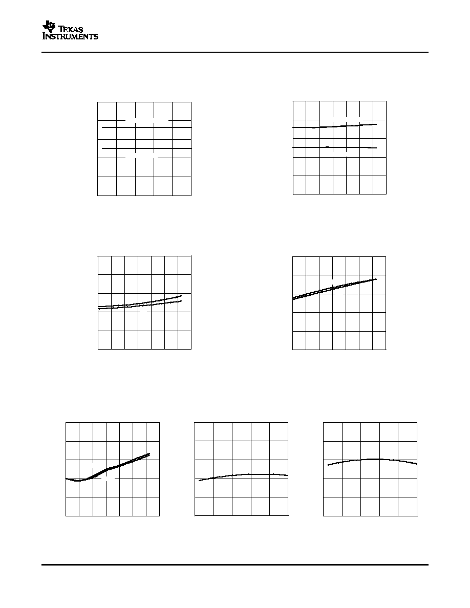
TYPICAL CHARACTERISTICS
-40
-20
0
20
40
60
80
100
65
55
45
35
25
15
I CC
- Supply Current - mA
T
A
- Free-Air Temperature - C
LVP16/17 = Load
LVDS16/17
15
25
35
45
55
65
0
400
800
1200
1600
2000
I CC
- Supply Current - mA
f - Frequency - MHz
LVP16/17 = Load
LVDS16/17
tr/tf - Rise/Fall Time - ps
T
A
- Free-Air Temperature - C
65
73
81
89
97
105
-40
-20
0
20
40
60
80
100
t
r
t
f
65
73
81
89
97
105
-40
-20
0
20
40
60
80
100
tr/tf - Rise/Fall Time - ps
T
A
- Free-Air Temperature - C
t
f
t
r
404
428
452
476
500
524
-40
-20
0
20
40
60
80
100
Propagation Delay Time - ps
T
A
- Free-Air Temperature - C
t
PLH
t
PHL
0
1
2
3
4
5
0
400
800
1200
1600
2000
Period Jitter - ps
f - Frequency - MHz
0
5
10
15
20
25
0
400
800
1200
1600
2000
Cycle-T
o-Cycle Jitter - ps
f - Frequency - MHz
SN65LVDS16, SN65LVP16
SN65LVDS17, SN65LVP17
SLLS625B ≠ SEPTEMBER 2004 ≠ REVISED NOVEMBER 2005
SUPPLY CURRENT
SUPPLY CURRENT
vs
vs
FREQUENCY
FREE-AIR TEMPERATURE
Figure 7.
Figure 8.
LVDS16/17 RISE/FALL TIME
LVP16/17 RISE/FALL TIME
vs
vs
FREE-AIR TEMPERATURE
FREE-AIR TEMPERATURE
Figure 9.
Figure 10.
LVDS16/17
PERIOD JITTER
CYCLE-TO-CYCLE JITTER
PROPAGATION DELAY TIME
vs
vs
vs
FREQUENCY
FREQUENCY
FREE-AIR TEMPERATURE
Figure 11.
Figure 12.
Figure 13.
9

www.ti.com
EQUIVALENT INPUT AND OUTPUT SCHEMATIC DIAGRAMS
R
R
Y
Z
V
CC
OUTPUT LVP16/17
V
CC
V
CC
7 V
7 V
V
CC
Y
Z
OUTPUT LVDS16/17
V
CC
7 V
7 V
V
CC
V
CC
300 k
400
7 V
ENABLE
A
B
V
CC
INPUT
V
CC
V
BB
V
CC
V
CC
V
BB
V
BB
OUTPUT
SN65LVDS16, SN65LVP16
SN65LVDS17, SN65LVP17
SLLS625B ≠ SEPTEMBER 2004 ≠ REVISED NOVEMBER 2005
10


PACKAGING INFORMATION
Orderable Device
Status
(1)
Package
Type
Package
Drawing
Pins Package
Qty
Eco Plan
(2)
Lead/Ball Finish
MSL Peak Temp
(3)
SN65LVDS16DRFR
ACTIVE
SON
DRF
8
3000 Green (RoHS &
no Sb/Br)
CU NIPDAU
Level-1-260C-UNLIM
SN65LVDS16DRFRG4
ACTIVE
SON
DRF
8
3000 Green (RoHS &
no Sb/Br)
CU NIPDAU
Level-1-260C-UNLIM
SN65LVDS16DRFT
ACTIVE
SON
DRF
8
250
Green (RoHS &
no Sb/Br)
CU NIPDAU
Level-1-260C-UNLIM
SN65LVDS16DRFTG4
ACTIVE
SON
DRF
8
250
Green (RoHS &
no Sb/Br)
CU NIPDAU
Level-1-260C-UNLIM
SN65LVDS17DRFR
ACTIVE
SON
DRF
8
3000 Green (RoHS &
no Sb/Br)
CU NIPDAU
Level-1-260C-UNLIM
SN65LVDS17DRFRG4
ACTIVE
SON
DRF
8
3000 Green (RoHS &
no Sb/Br)
CU NIPDAU
Level-1-260C-UNLIM
SN65LVDS17DRFT
ACTIVE
SON
DRF
8
250
Green (RoHS &
no Sb/Br)
CU NIPDAU
Level-1-260C-UNLIM
SN65LVDS17DRFTG4
ACTIVE
SON
DRF
8
250
Green (RoHS &
no Sb/Br)
CU NIPDAU
Level-1-260C-UNLIM
SN65LVP16DRFR
ACTIVE
SON
DRF
8
3000 Green (RoHS &
no Sb/Br)
CU NIPDAU
Level-1-260C-UNLIM
SN65LVP16DRFRG4
ACTIVE
SON
DRF
8
3000 Green (RoHS &
no Sb/Br)
CU NIPDAU
Level-1-260C-UNLIM
SN65LVP16DRFT
ACTIVE
SON
DRF
8
250
Green (RoHS &
no Sb/Br)
CU NIPDAU
Level-1-260C-UNLIM
SN65LVP16DRFTG4
ACTIVE
SON
DRF
8
250
Green (RoHS &
no Sb/Br)
CU NIPDAU
Level-1-260C-UNLIM
SN65LVP17DRFR
ACTIVE
SON
DRF
8
3000 Green (RoHS &
no Sb/Br)
CU NIPDAU
Level-1-260C-UNLIM
SN65LVP17DRFRG4
ACTIVE
SON
DRF
8
3000 Green (RoHS &
no Sb/Br)
CU NIPDAU
Level-1-260C-UNLIM
SN65LVP17DRFT
ACTIVE
SON
DRF
8
250
Green (RoHS &
no Sb/Br)
CU NIPDAU
Level-1-260C-UNLIM
SN65LVP17DRFTG4
ACTIVE
SON
DRF
8
250
Green (RoHS &
no Sb/Br)
CU NIPDAU
Level-1-260C-UNLIM
(1)
The marketing status values are defined as follows:
ACTIVE: Product device recommended for new designs.
LIFEBUY: TI has announced that the device will be discontinued, and a lifetime-buy period is in effect.
NRND: Not recommended for new designs. Device is in production to support existing customers, but TI does not recommend using this part in
a new design.
PREVIEW: Device has been announced but is not in production. Samples may or may not be available.
OBSOLETE: TI has discontinued the production of the device.
(2)
Eco
Plan
-
The
planned
eco-friendly
classification:
Pb-Free
(RoHS)
or
Green
(RoHS
&
no
Sb/Br)
-
please
check
http://www.ti.com/productcontent
for the latest availability information and additional product content details.
TBD: The Pb-Free/Green conversion plan has not been defined.
Pb-Free (RoHS): TI's terms "Lead-Free" or "Pb-Free" mean semiconductor products that are compatible with the current RoHS requirements
for all 6 substances, including the requirement that lead not exceed 0.1% by weight in homogeneous materials. Where designed to be soldered
at high temperatures, TI Pb-Free products are suitable for use in specified lead-free processes.
Green (RoHS & no Sb/Br): TI defines "Green" to mean Pb-Free (RoHS compatible), and free of Bromine (Br) and Antimony (Sb) based flame
retardants (Br or Sb do not exceed 0.1% by weight in homogeneous material)
(3)
MSL, Peak Temp. -- The Moisture Sensitivity Level rating according to the JEDEC industry standard classifications, and peak solder
temperature.
PACKAGE OPTION ADDENDUM
www.ti.com
17-Nov-2005
Addendum-Page 1

Important Information and Disclaimer:The information provided on this page represents TI's knowledge and belief as of the date that it is
provided. TI bases its knowledge and belief on information provided by third parties, and makes no representation or warranty as to the
accuracy of such information. Efforts are underway to better integrate information from third parties. TI has taken and continues to take
reasonable steps to provide representative and accurate information but may not have conducted destructive testing or chemical analysis on
incoming materials and chemicals. TI and TI suppliers consider certain information to be proprietary, and thus CAS numbers and other limited
information may not be available for release.
In no event shall TI's liability arising out of such information exceed the total purchase price of the TI part(s) at issue in this document sold by TI
to Customer on an annual basis.
PACKAGE OPTION ADDENDUM
www.ti.com
17-Nov-2005
Addendum-Page 2


IMPORTANT NOTICE
Texas Instruments Incorporated and its subsidiaries (TI) reserve the right to make corrections, modifications,
enhancements, improvements, and other changes to its products and services at any time and to discontinue
any product or service without notice. Customers should obtain the latest relevant information before placing
orders and should verify that such information is current and complete. All products are sold subject to TI's terms
and conditions of sale supplied at the time of order acknowledgment.
TI warrants performance of its hardware products to the specifications applicable at the time of sale in
accordance with TI's standard warranty. Testing and other quality control techniques are used to the extent TI
deems necessary to support this warranty. Except where mandated by government requirements, testing of all
parameters of each product is not necessarily performed.
TI assumes no liability for applications assistance or customer product design. Customers are responsible for
their products and applications using TI components. To minimize the risks associated with customer products
and applications, customers should provide adequate design and operating safeguards.
TI does not warrant or represent that any license, either express or implied, is granted under any TI patent right,
copyright, mask work right, or other TI intellectual property right relating to any combination, machine, or process
in which TI products or services are used. Information published by TI regarding third-party products or services
does not constitute a license from TI to use such products or services or a warranty or endorsement thereof.
Use of such information may require a license from a third party under the patents or other intellectual property
of the third party, or a license from TI under the patents or other intellectual property of TI.
Reproduction of information in TI data books or data sheets is permissible only if reproduction is without
alteration and is accompanied by all associated warranties, conditions, limitations, and notices. Reproduction
of this information with alteration is an unfair and deceptive business practice. TI is not responsible or liable for
such altered documentation.
Resale of TI products or services with statements different from or beyond the parameters stated by TI for that
product or service voids all express and any implied warranties for the associated TI product or service and
is an unfair and deceptive business practice. TI is not responsible or liable for any such statements.
Following are URLs where you can obtain information on other Texas Instruments products and application
solutions:
Products
Applications
Amplifiers
amplifier.ti.com
Audio
www.ti.com/audio
Data Converters
dataconverter.ti.com
Automotive
www.ti.com/automotive
DSP
dsp.ti.com
Broadband
www.ti.com/broadband
Interface
interface.ti.com
Digital Control
www.ti.com/digitalcontrol
Logic
logic.ti.com
Military
www.ti.com/military
Power Mgmt
power.ti.com
Optical Networking
www.ti.com/opticalnetwork
Microcontrollers
microcontroller.ti.com
Security
www.ti.com/security
Telephony
www.ti.com/telephony
Video & Imaging
www.ti.com/video
Wireless
www.ti.com/wireless
Mailing Address:
Texas Instruments
Post Office Box 655303 Dallas, Texas 75265
Copyright
2005, Texas Instruments Incorporated