 | ÐлекÑÑоннÑй компоненÑ: P82B96 | СкаÑаÑÑ:  PDF PDF  ZIP ZIP |
P82B96
www.ti.com
FEATURES
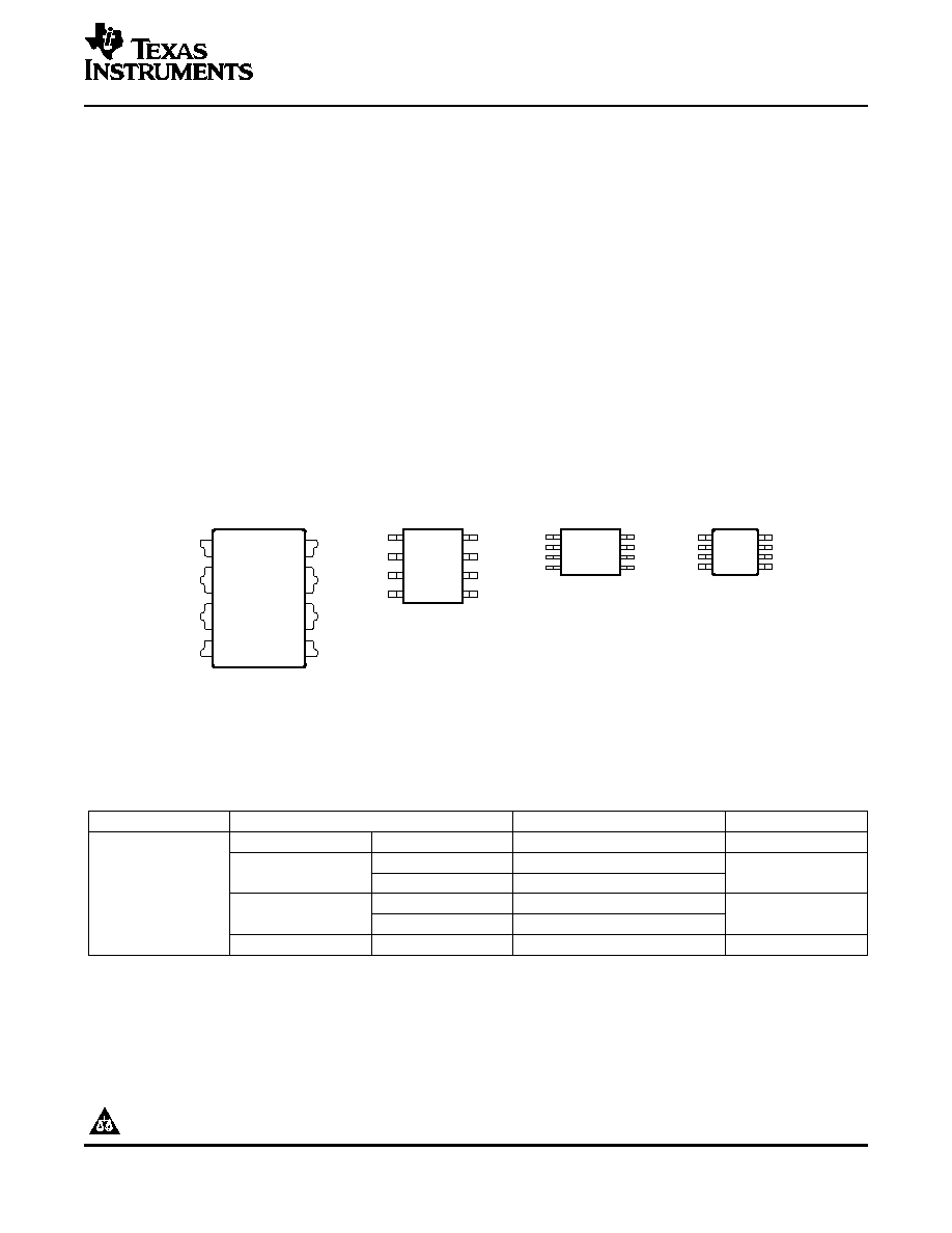
D PACKAGE
(TOP VIEW)
GND
1
2
3
4
5
6
7
8
Sx
Rx
Tx
Ty
Ry
Sy
V
CC
P PACKAGE
(TOP VIEW)
1
2
3
4
5
6
7
8
Sx
Rx
Tx
GND
Ty
Ry
Sy
V
CC
DGK PACKAGE
(TOP VIEW)
1
2
3
4
5
6
7
8
Ty
Ry
Sy
V
CC
Sx
Rx
Tx
GND
PW PACKAGE
(TOP VIEW)
1
2
3
4
5
6
7
8
Sx
Rx
Tx
GND
Ty
Ry
Sy
V
CC
DESCRIPTION/ORDERING INFORMATION
P82B96
DUAL BIDIRECTIONAL BUS BUFFER
SCPS144 MAY 2006
·
Operating Power-Supply Voltage Range
·
400-kHz Fast I
2
C Bus Operation Over at Least
of 2 V to 15 V
20 Meters of Wire
·
Can Interface Between I
2
C Buses Operating
·
Low Standby Current Consumption
at Different Logic Levels (2 V to 15 V)
·
Latch-Up Performance Exceeds 100 mA Per
·
Supports Bidirectional Data Transfer of I
2
C
JESD 78, Class II
Bus Signals
·
ESD Protection Exceeds JESD 22
·
Allows bus capacitance of 400 pF on the
3500-V Human-Body Model (A114-A)
Main I
2
C Bus (Sx/Sy Side) and 4000 pF on the
200-V Machine Model (A115-A)
Transmission Side (Tx/Ty)
1000-V Charged-Device Model (C101)
·
Outputs on the Transmission Side (Tx/Ty)
Have High Sink Capability for Driving
Low-Impedance or High-Capacitive Buses
·
I
2
C Bus Signals Can Be Split Into Pairs of
Forward (Tx/Ty) and Reverse (Rx/Ry) Signals
for Interface With Optoelectrical Isolators and
Similar Devices That Need Unidirectional
Input and Output Signal Paths
The P82B96 is a bipolar device that supports bidirectional data transfer between the normal I
2
C bus and a range
of other bus configurations with different voltage and current levels. It can function as the interface without any
limitations on the normal I
2
C operation and clock speed.
ORDERING INFORMATION
T
A
PACKAGE
(1)
ORDERABLE PART NUMBER
TOP-SIDE MARKING
PDIP P
Tube of 50
P82B96P
P82B96P
Reel of 2000
P82B96DR
SOIC D
PG96
Tube of 75
P82B96D
40
°
C to 85
°
C
Reel of 2000
P82B96PWR
TSSOP PW
PG96
Tube of 150
P82B96PW
VSSOP DGK
Reel of 2500
P82B96DGKR
7DS
(1)
Package drawings, standard packing quantities, thermal data, symbolization, and PCB design guidelines are available at
www.ti.com/sc/package.
Please be aware that an important notice concerning availability, standard warranty, and use in critical applications of Texas
Instruments semiconductor products and disclaimers thereto appears at the end of this data sheet.
PRODUCTION DATA information is current as of publication date.
Copyright © 2006, Texas Instruments Incorporated
Products conform to specifications per the terms of the Texas
Instruments standard warranty. Production processing does not
necessarily include testing of all parameters.
www.ti.com
DESCRIPTION/ORDERING INFORMATION (CONTINUED)
P82B96
DUAL BIDIRECTIONAL BUS BUFFER
SCPS144 MAY 2006
One of the advantages of the P82B96 is that it can isolate bus capacitance such that the total loading (devices
and trace lengths) of the new bus or remote I
2
C nodes are not apparent to other I
2
C buses (or nodes). This
device also adds minimal loading to I
2
C node where it is positioned. Any restrictions on the number of I
2
C
devices in a system, or the physical separation between them, are virtually eliminated.
The P82B96 easily can transmit SDA/SCL signals via balanced transmission lines (twisted pairs) or with
galvanic isolation (optocoupling), because separate directional Tx and Rx signals are provided. The Tx and Rx
signals may be connected directly (without causing bus latching), to provide an alternative bidirectional signal
line with I
2
C properties.
Two or more Sx or Sy I/Os must not be interconnected. The P82B96 design does not support this configuration.
Bidirectional I
2
C signals do not allow any direction control pin so, instead, slightly different logic low-voltage
levels are used at Sx/Sy to avoid latching of this buffer. A regular I
2
C low applied at the Rx/Ry of a P82B96 is
propagated to Sx/Sy as a buffered low with a slightly higher voltage level. If this special buffered low is applied
to the Sx/Sy of another P82B96, the second P82B96 does not recognize it as a regular I
2
C bus low and does
not propagate it to its Tx/Ty output. The Sx/Sy side of P82B96 may not be connected to similar buffers that rely
on special logic thresholds for their operation, such as the PCA9515A.
The Sx/Sy side is intended only for, and compatible with, the normal I
2
C logic voltage levels of I
2
C master and
slave devices or Tx/Rx signals of a second P82B96, if required. The Tx/Rx and Ty/Ry I/O pins use the standard
I
2
C logic voltage levels of all I
2
C parts. If Rx and Tx are connected, Sx can function as either the SDA or SCL
line. Similarly, if Ry and Ty are connected, Sy can function as either the SDA or SCL line. There are no
restrictions on the interconnection of the Tx/Rx and Ty/Ry I/O pins to other P82B96s, for example in a star or
multi-point configuration with the Tx/Rx and Ty/Ry I/O pins on the common bus, and the Sx/Sy side connected
to the line-card slave devices.
TERMINAL FUNCTIONS
NO.
NAME
DESCRIPTION
1
Sx
Serial data bus or SDA. Connect to V
CC
of I
2
C master through a pullup resistor.
2
Rx
Receive signal. Connect to V
CC
of P82B96 through a pullup resistor.
3
Tx
Transmit signal. Connect to V
CC
of P82B96 through a pullup resistor.
4
GND
Ground
5
Ty
Transmit signal. Connect to V
CC
of P82B96 through a pullup resistor.
6
Ry
Receive signal. Connect to V
CC
of P82B96 through a pullup resistor.
7
Sy
Serial clock bus or SCL. Connect to V
CC
of I
2
C master through a pullup resistor.
8
V
CC
Supply voltage
2
Submit Documentation Feedback
www.ti.com
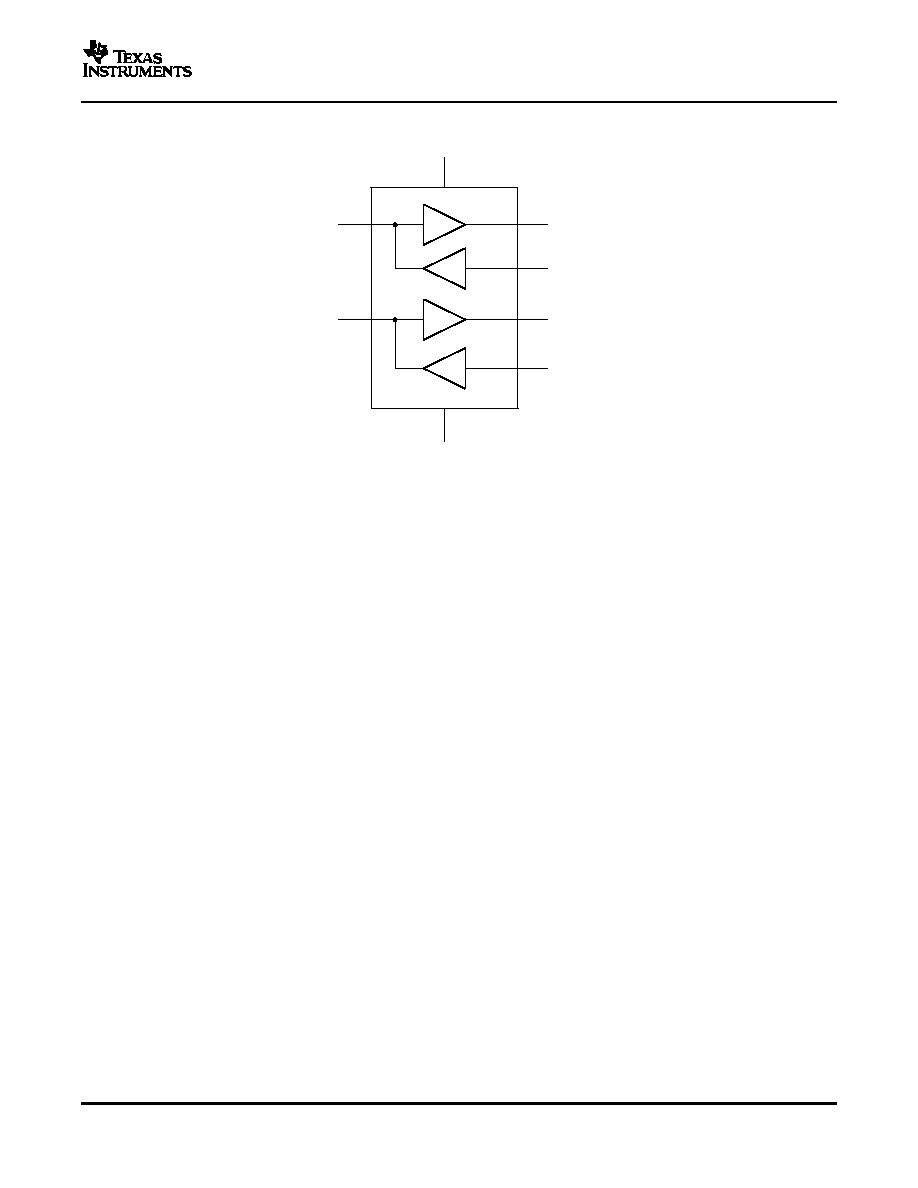
P82B96
Sx (SDA)
Sy (SCL)
Ry (RxD, SCL)
Ty (TxD, SCL)
Rx (RxD, SDA)
Tx (TxD, SDA)
1
7
4
GND
6
5
2
3
8
V
(2!15 V)
CC
Functional Description
Sx and Sy
Tx and Ty
P82B96
DUAL BIDIRECTIONAL BUS BUFFER
SCPS144 MAY 2006
FUNCTIONAL BLOCK DIAGRAM
The I
2
C pins, Sx and Sy, are designed to interface with a normal I
2
C bus. The logic threshold-voltage levels on
the I
2
C bus are independent of the supply V
CC
. The maximum I
2
C bus supply voltage is 15 V, and the specified
static sink current is 3 mA.
Sx and Sy have two identical buffers. Each buffer is made up of two logic signal paths. The first one, named Tx
or Ty, is a forward path from the I
2
C interface pin, which drives the buffered bus. The second one, named Rx or
Ry, is a reverse signal path from the buffered bus input to drive the I
2
C bus interface.
There are two purposes for these paths: to sense the voltage state of the I
2
C pin (Sx or Sy) and transmit this
state to Tx or Ty, respectively, and to detect the state of the Rx or Ry and pull the I
2
C pin low when Rx or Ry is
low.
Tx and Ty are open-collector outputs without ESD protection diodes to V
CC
. Each pin may be connected via a
pullup resistor to a supply voltage in excess of V
CC
, as long as the 15-V rating is not exceeded. Tx and Ty have
a larger current-sinking capability than a normal I
2
C device and can sink a static current of greater than 30 mA.
They also have dynamic pulldown capability of 100-mA, typically.
A logic low is transmitted to Tx or Ty only when the voltage at the I
2
C pin (Sx or Sy) is below 0.6 V. A logic low
at Rx or Ry causes the I
2
C bus (Sx or Sy) to be pulled to a logic low level in accordance with I
2
C requirements
(maximum 1.5 V in 5-V applications), but not low enough to be looped back to the Tx or Ty output and cause the
buffer to latch low.
The minimum low level that the P82B96 can achieve on the I
2
C bus by a low at Rx or Ry typically is 0.8 V.
If V
CC
fails, neither the I
2
C pins nor the Tx or Ty outputs are held low. Their open-collector configuration allows
them to be pulled up to the rated maximum of 15 V without V
CC
present. The input configuration on Sx, Sy, Rx,
and Ry also presents no loading of external signals when V
CC
is not present.
The effective input capacitance of any signal pin, measured by its effect on bus rise times, is less than 4 pF for
all bus voltages and supply voltages, including V
CC
= 0 V.
3
Submit Documentation Feedback
www.ti.com
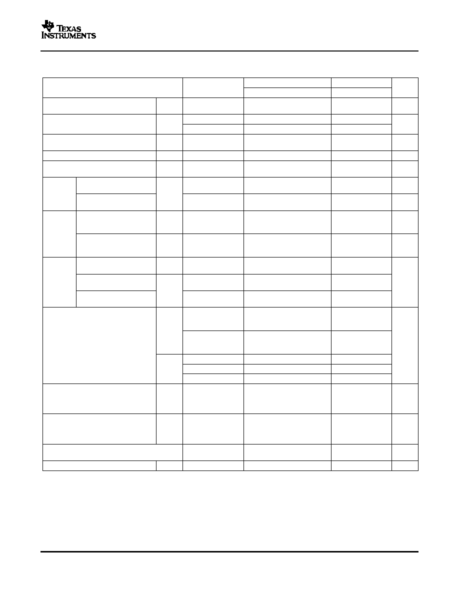
Absolute Maximum Ratings
(1)
Recommended Operating Conditions
P82B96
DUAL BIDIRECTIONAL BUS BUFFER
SCPS144 MAY 2006
over operating free-air temperature range (unless otherwise noted)
MIN
MAX
UNIT
V
CC
Supply voltage range
0.3
18
V
Sx or Sy (SDA or SCL)
0.3
18
V
I
Voltage range on buffered input
V
Rx or Ry
0.3
18
Sx or Sy (SDA or SCL)
0.3
18
V
O
Voltage range on buffered output
V
Tx or Ty
0.3
18
Sx or Sy
250
I
O
Continuous output current
mA
Tx or Ty
250
I
CC
Continuous current through V
CC
or GND
250
mA
D package
97
P package
85
JA
Package thermal impedance
(2)
°
C/W
PW package
149
DGK package
172
T
stg
Storage temperature range
55
125
°
C
T
A
Operating free-air temperature range
40
85
°
C
(1)
Stresses beyond those listed under Absolute Maximum Ratings may cause permanent damage to the device. These are stress ratings
only, and functional operation of the device at these or any other conditions beyond those indicated under Recommended Operating
Conditions is not implied. Exposure to absolute-maximum-rated conditions for extended periods may affect device reliability.
(2)
The package thermal impedance is calculated in accordance with JESD 51-7.
MIN
MAX
UNIT
V
CC
Supply voltage
2
15
V
V
Sx
, V
Sy
= 1 V,
Sx, Sy
3
V
Rx
, V
Ry
0.42 V
I
OL
Low-level output current
mA
V
Sx
, V
Sy
= 0.4 V,
Tx, Ty
30
V
Tx
, V
Ty
= 0.4 V
Sx, Sy
V
Tx
, V
Ty
= 0.4 V
15
V
IOmax
Maximum input/output voltage level
V
Tx, Ty
V
Sx
, V
Sy
= 0.4 V
15
V
ILdiff
Low-level input voltage difference
Sx, Sy
0.4
V
T
A
Operating free-air temperature
40
85
°
C
4
Submit Documentation Feedback
www.ti.com
Electrical Characteristics
P82B96
DUAL BIDIRECTIONAL BUS BUFFER
SCPS144 MAY 2006
V
CC
= 2.3 V to 2.7 V, voltages are specified with respect to GND (unless otherwise noted)
T
A
= 25
°
C
T
A
= 40
°
C to 85
°
C
TEST
PARAMETER
UNIT
CONDITIONS
MIN
TYP
(1)
MAX
MIN
MAX
Temperature coefficient of
V/
T
IN
Sx, Sy
2
mV/
°
C
input thresholds
I
Sx
, I
Sy
= 3 mA
0.8
0.88
1
See
Figure 6
V
OL
Low-level output voltage
Sx, Sy
V
I
Sx
, I
Sy
= 0.2 mA
0.67
0.73
0.79
See
Figure 5
Temperature coefficient of
V/
T
OUT
Sx, Sy
I
Sx
, I
Sy
= 0.2 mA
1.8
mV/
°
C
output low levels
(2)
I
CC
Quiescent supply current
Sx = Sy = V
CC
0.9
1.8
2
mA
Additional supply current
I
CC
Tx, Ty
1.7
2.75
3
mA
per pin low
Dynamic output sink
V
Sx
, V
Sy
> 2 V,
7
18
5.5
mA
capability on I
2
C bus
V
Rx
, V
Ry
= low
I
IOS
Sx, Sy
V
Sx
, V
Sy
= 2.5 V,
Leakage current on I
2
C bus
0.1
1
1
µ
A
V
Rx
, V
Ry
= high
V
Tx
, V
Ty
> 1 V,
Dynamic output sink
Tx, Ty
V
Sx
, V
Sy
= low on
60
100
60
mA
capability on buffered bus
I
2
C bus = 0.4 V
I
IOT
V
Tx
, V
Ty
= V
CC
=
Leakage current
2.5 V,
0.1
1
1
µ
A
on buffered bus
V
Sx
, V
Sy
= high
Bus low, V
Rx
,
Input current from I
2
C bus
Sx, Sy
1
1
V
Ry
= high
Input current
Bus low, V
Rx
,
I
I
1
1
µ
A
from buffered bus
V
Ry
= 0.4 V
Rx, Ry
Leakage current
V
Rx
, V
Ry
= V
CC
1
1.5
on buffered bus input
Input logic level high
threshold
(3)
0.65
0.7
See
Figure 8
on normal I
2
C bus
Sx, Sy
Input logic level low
threshold
(3)
0.6
0.65
See
Figure 7
V
IT
Input threshold
V
on normal I
2
C bus
Input logic level high
0.58 V
CC
0.58 V
CC
Rx, Ry
Input threshold
0.5 V
CC
Input logic level low
0.42 V
CC
0.42 V
CC
(V
Sx
output low
Input/output logic level
at 3 mA)
V
IOdiff
Sx, Sy
100
150
100
mV
difference
(4)
(V
Sx
input high max)
for I
2
C applications
Sx, Sy are low, V
CC
V
CC
voltage at which all
Sx, Sy
ramping, voltage on
V
IOrel
1
1
V
buses are released
Tx, Ty
Tx, Ty lowered until
released
Temperature coefficient of release
V/
T
REL
4
mV/K
voltage
C
in
Input capacitance
Rx, Ry
2.5
4
4
pF
(1)
Typical value is at V
CC
= 2.5 V, T
A
= 25
°
C
(2)
The output logic low depends on the sink current.
(3)
The input logic threshold is independent of the supply voltage.
(4)
The minimum value requirement for pullup current, 200
µ
A, ensures that the minimum value for V
SX
output low always exceeds the
minimum V
Sx
input high level to eliminate any possibility of latching. The specified difference is specified by design within any device.
While the tolerances on absolute levels allow a small probability that the low from one Sx output is recognized by an Sx input of another
P82B96, this has no consequences for normal applications. In any design, the Sx pins of different devices should never be linked,
because the resulting system would be very susceptible to induced noise and would not support all I
2
C operating modes.
5
Submit Documentation Feedback
Document Outline