 | ÐлекÑÑоннÑй компоненÑ: MAX5914A | СкаÑаÑÑ:  PDF PDF  ZIP ZIP |
MAX5913A/14A DS
General Description
The MAX5913A/MAX5914A are quadruple hot-swap con-
trollers. The MAX5913A/MAX5914A independently con-
trol four external n-channel switches to hot-swap system
loads from a single V
CC
supply line. The devices allow
the safe insertion and removal of power devices from live
network ports. The operating supply voltage range is
between +35V and +72V. The devices are intended for
applications in Power-Over-Media-Dependent Interface
(MDI), but are not limited to such usage.
The MAX5913A/MAX5914A feature an internal under-
voltage lockout (UVLO) function that prevents the FET
from turning on, if V
CC
does not exceed the default
value of +32V. The devices also feature a +12V relay
driver with 100mA current drive capable of driving low-
voltage +3.3V relays. The MAX5913A features an
active-low relay driver that sinks current when the relay
output is enabled. The MAX5914A features an active-
high relay driver output that sources 1mA to drive an
external FET relay driver when the relay output is
enabled. Control circuitry ensures the relays and the
FETs are off until V
CC
reaches the UVLO threshold. The
MAX5913A/MAX5914A use an external sense resistor
to enable all the internal current-sense functions.
The MAX5913A/MAX5914A feature a programmable
analog current-limit circuit. If the switch remains in current
limit for more than a programmable time, the n-channel
FET latches off and the supply can be restarted either by
autoretry or by an external command after the preset off-
time has elapsed.
The MAX5913A/MAX5914A are available in a 44-pin
MQFP package and are specified for the extended
-40°C to +85°C operating temperature range.
Applications
Power-Over-LAN
Power-Over-MDI
IP Phone Switches/Routers
Telecom Line Cards
Network Switches/Routers
Midspan Power-Over-MDI
Features
Wide Operating Input Voltage Range:
+35V to +72V
IEEE 802.3af Compatible
Four Independent Power Switch Controllers
Open-Circuit Detector
On-Board Charge Pumps to Drive External
n-Channel FETs
Current Sense with External Resistor
Foldback Current Limiting
+32V Input Undervoltage Lockout
On-Chip +12V, 100mA Voltage Relay Drivers
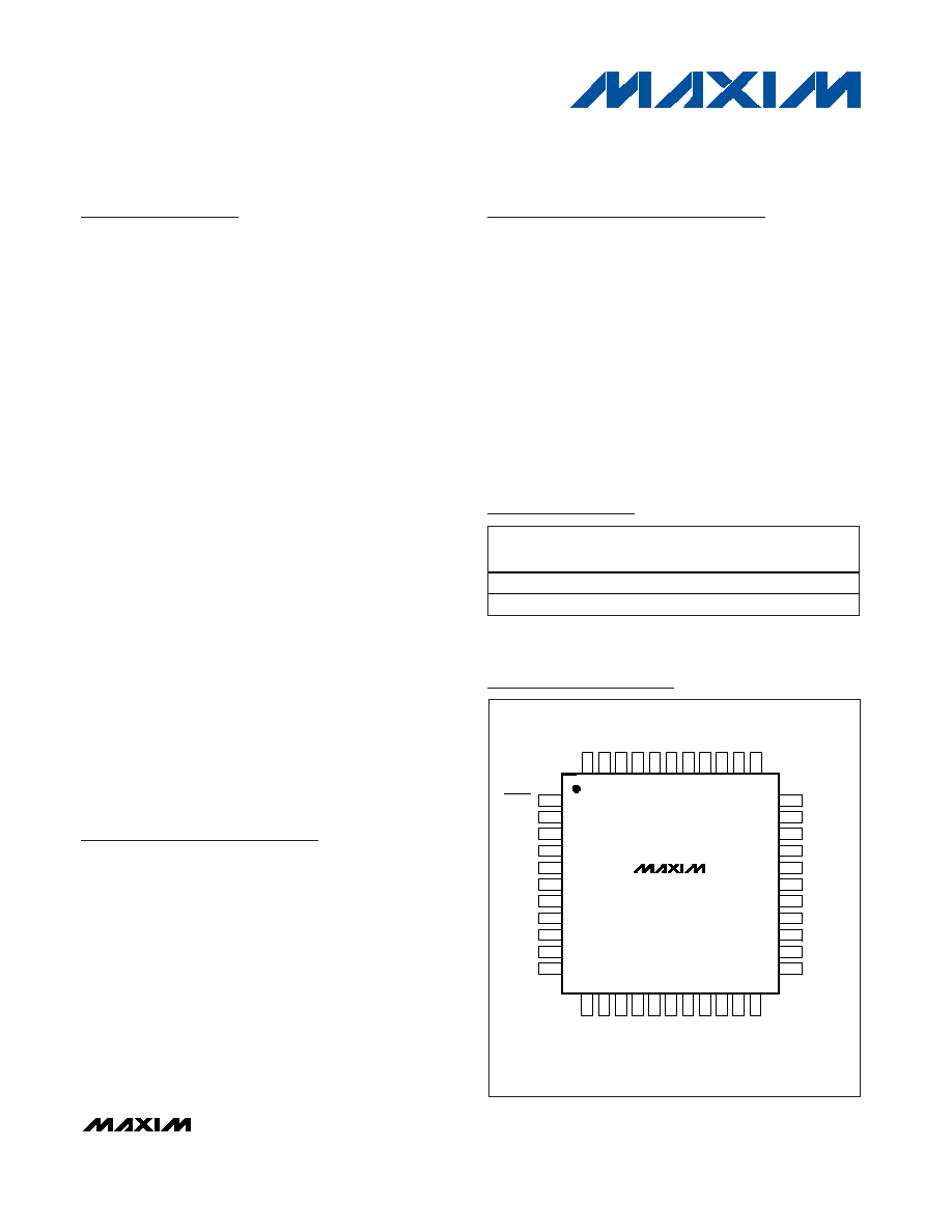
MAX5913A/MAX5914A
+48V Quad Hot-Swap Controllers For
Power-Over-LAN
________________________________________________________________ Maxim Integrated Products
1
RTRYEN
STATOUT
OCEN
DGND
V
CC
CSP1
DRAIN1
GATE1
OUT1
CSP2
DRAIN2
FAULT
STAT1
STAT2
STAT3
STAT4
CSP4
DRAIN4
OUT4
GATE4
CSP3
DRAIN3
1
2
3
4
5
6
7
8
9
10
11
12
13
14
15
16
17
18
19
20
21
22
44
43
42
41
40
39
38
37
36
35
34
33
32
31
30
29
28
27
26
25
24
23
OUT3
GATE3
V
RLY
RLYD3
RLYD4
DGND
RLYD1
RLYD2
AGND
OUT2
GATE2
V
DD
RTIM
ON4
RLYON4
ON3
RLYON3
ON2
RLYON2
ON1
RLYON1
DC
MQFP
TOP VIEW
MAX5913A
MAX5914A
Pin Configuration
Ordering Information
19-3302; Rev 0; 5/04
For pricing, delivery, and ordering information, please contact Maxim/Dallas Direct! at
1-888-629-4642, or visit Maxim's website at www.maxim-ic.com.
PART
TEMP RANGE
PIN-
PACKAGE
PKG
CODE
MAX5913AEMH
-40°C to +85°C
44 MQFP
M44-3
MAX5914AEMH*
-40°C to +85°C
44 MQFP
M44-3
Typical Operating Circuit appears at end of data sheet.
*Future product--contact factory for availability.
MAX5913A/MAX5914A
+48V Quad Hot-Swap Controllers For
Power-Over-LAN
2
_______________________________________________________________________________________
ABSOLUTE MAXIMUM RATINGS
ELECTRICAL CHARACTERISTICS
(V
CC
= V
CSP
_ = +48V, AGND = DGND = 0V, V
DD
= +3.3V, V
RLY
= +12V, T
A
= -40°C to +85°C, unless otherwise noted. Typical val-
ues are at V
CC
= V
CSP
_ = +48V and T
A
= +25°C.)
Stresses beyond those listed under "Absolute Maximum Ratings" may cause permanent damage to the device. These are stress ratings only, and functional
operation of the device at these or any other conditions beyond those indicated in the operational sections of the specifications is not implied. Exposure to
absolute maximum rating conditions for extended periods may affect device reliability.
V
CC
to AGND or DGND..........................................-0.6V to +76V
DRAIN_, OUT_ to AGND or DGND .............-0.6V to (V
CC
+0.3V)
CSP_ to V
CC
..........................................................-0.3V to +0.3V
GATE_ to OUT_ .....................................................-0.3V to +13V
V
RLY
to DGND ........................................................-0.3V to +18V
RLYD_ to DGND........................................-0.3V to (V
RLY
+ 0.3V)
ON_, RLYON_, OCEN, RTRYEN, STATOUT,
DC to DGND........................................................-0.3V to +12V
FAULT to DGND .....................................................-0.3V to +12V
STAT_, RTIM to DGND ...............................-0.3V to (V
DD
+ 0.3V)
V
DD
to DGND ...........................................................-0.3V to +7V
DGND to AGND...........................................................-5V to +5V
Current into RLYD_ .........................................-50mA to +150mA
Current into Any Other Pin................................................±50mA
Continuous Power Dissipation (T
A
= +70°C)
44-Pin MQFP (derate 12.7mW/°C above +70°C)......... 1.013W
Operating Temperature Range ...........................-40°C to +85°C
Storage Temperature Range .............................-65°C to +150°C
Lead Temperature (soldering, 10s) ................................ +300°C
PARAMETER
SYMBOL
CONDITIONS
MIN
TYP
MAX
UNITS
POWER SUPPLIES
Analog Supply Voltage
V
CC
Measured with respect to AGND
35
72
V
T
A
= 0°C to +85°C
2.7
4
Analog Supply Current
I
S
V
CC
= V
CSP
_ = 72V
I
S
= I
CC
+ I
CSP
T
A
= -40°C to 0°C
5
mA
Digital Supply Voltage
V
DD
Measured with respect to DGND
2.5
3.3
3.7
V
Digital Supply Current
I
DD
All logic outputs high, RTIM floating
1.1
3
mA
Analog Supply Undervoltage
Lockout
V
UVLO
V
CC
rising, circuits enabled
29
32
35
V
UVLO Hysteresis
V
UVLO,H
3
V
UVLO Deglitch Delay
t
D,UVLO
V
ON
= 3.3V, V
RLYON
= 3.3V (Figure 1)
12.8
25.6
38.4
ms
Relay Driver Supply
V
RLY
Measured with respect to DGND
14
V
Ground Potential Difference
V
GG
Voltage difference between DGND and AGND
-4
4
V
FEEDBACK INPUT AND CURRENT SENSE
OUT Sense Bias Current
I
FP
V
OUT
_ = V
CC
2
µA
Initial Feedback Voltage
V
FB
_
S
Voltage under which the foldback circuit starts
reducing the current-limit value
(Note 1)
18
V
Current-Limit Threshold Voltage
V
SC
Maximum
V across R
SENSE
at V
OUT
> V
FB
_
S
125
142.5
160
mV
Foldback Voltage
V
FLBK
Maximum
V across R
SENSE
at V
OUT
= 0V
42
48
54
mV
Fast Discharge Threshold
V
FC
360
420
480
mV
Switch-On Threshold
V
SWON
Maximum V
CC
- V
OUT
at which the switch is
defined as fully on, V
OUT
increasing
1.2
1.5
1.8
V
Switch-On Comparator Hysteresis
V
SWON
_
H
160
mV
MOSFET DRIVERS
V
GATE
- V
CC
when switch is fully on
0
°C to +85°C
7
9
11
Gate Overdrive Voltage
V
GS
T
A
= -40
°C to 0°C
7
9
12
V
Gate Charge Current
I
GATE
V
GATE
= 0V
7
10
13
µA

MAX5913A/MAX5914A
+48V Quad Hot-Swap Controllers For
Power-Over-LAN
_______________________________________________________________________________________
3
ELECTRICAL CHARACTERISTICS (continued)
(V
CC
= V
CSP
_ = +48V, AGND = DGND = 0V, V
DD
= +3.3V, V
RLY
= +12V, T
A
= -40°C to +85°C, unless otherwise noted. Typical val-
ues are at V
CC
= V
CSP
_ = +48V and T
A
= +25°C.) (Note 3)
Note 1: See Typical Operating Characteristics for Current-Limit Foldback, and refer to Current Sensing and Regulation section.
Note 2: The resistor at RTIM can range from 2k to 40k.
Note 3: Limits are 100% tested at T
A
= +25°C and T
A
= +85°C. Limits at -40°C are guaranteed by design and characterization, but
are not production tested.
PARAMETER
SYMBOL
CONDITIONS
MIN
TYP
MAX
UNITS
During current regulation
8
µA
V
ON
= 0V
1
mA
Gate Discharge Current
I
GATE
,
DIS
(V
CSP
_ - V
DRAIN
_) > V
FC
15
mA
Source-Gate Clamp Voltage
V
SGZ
V
OUT
_ = 0V, force 30mA into GATE_,
measure V
GATE
- V
OUT
14
16.5
18
V
OPEN-CIRCUIT DETECTOR
Open-Circuit Current-Threshold
Voltage
V
OC
Minimum V across R
SENSE
to detect an
open circuit
1.5
3
4.5
mV
Delay to Open-Circuit Detect
t
OC
(Figure 2)
450
900
1350
ms
Deglitch Delay
t
LPFD
(V
CSP
_ - V
DRAIN
__
) < V
OC
(Figure 2)
106
204
302
ms
RELAY DRIVERS
Maximum Low Voltage (MAX5913A)
V
RLOW
RLYON = high, I
RLYD
_ = 100mA
0.5
V
Relay Pullup Current (MAX5914A)
I
RPLUP
RLYON = high, V
RLYD
_ = 0V
0.3
0.8
1.3
mA
Clamp Diode Voltage
V
RCLAMP
Force 100mA into RLYD, measure V
RLYD
-
V
RLY
2
V
Relay Output Leakage
RLYON_ = low, V
RLYD
_ = V
RLY
1
µA
TIMING
R
RTIM
= 2k
4.8
6.4
8.0
R
RTIM
= 40k
76
128
180
Short-Circuit and Startup Timer
(Note 2)
t
O
On time for continuous
overcurrent conditions
R
RTIM
=
3.2
6.4
9.6
ms
DC = logic low
1
DC = logic high
2
Auto-Retry Duty Cycle
DC = floating
4
%
Port Turn-On Delay
t
ON
_
DEL
V
ON
= 3.3V (Figure 3)
12.8
25.6
38.4
ms
Relay Turn-Off Delay
t
OFF
_
DEL
After RLYON_ goes low (Figure 3)
1.6
3.2
4.8
ms
DIGITAL INTERFACE
DC Pin Input-Voltage High
V
IH
_
DC
2.5V V
DD
3.7V
0.7 x V
DD
V
DC Pin Input-Voltage Low
V
IL
_
DC
2.5V V
DD
3.7V
0.3 x V
DD
V
DC Pin Input Impedance
R
IN
_
DC
1
k
Logic Input High
V
IH
2.5V V
DD
3.7V
0.8 x V
DD
V
Logic Input Low
V
IL
2.5V V
DD
3.7V
0.3 x V
DD
V
Logic Input Leakage
1
µA
FAULT Output-Voltage Low
V
FL
I
SINK
= 4mA
0.4
V
FAULT High Input Leakage
1
µA
Logic Output-Voltage High
V
OH
STAT_ outputs sourcing 0.5mA
V
DD
- 0.4
mV
Logic Output-Voltage Low
V
OL
STAT_ outputs sinking 0.5mA
0.4
V
MAX5913A/MAX5914A
+48V Quad Hot-Swap Controllers For
Power-Over-LAN
4
_______________________________________________________________________________________
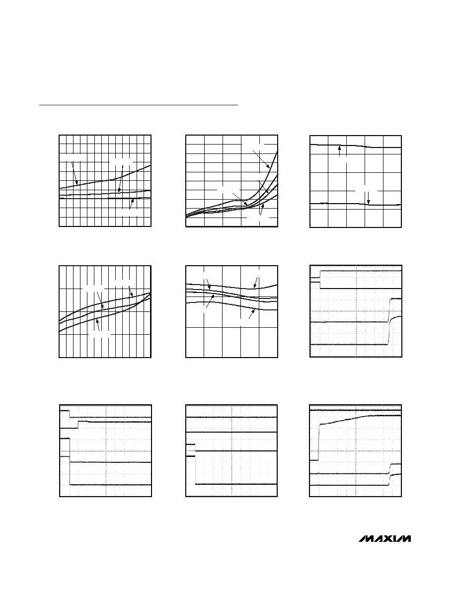
Typical Operating Characteristics
(V
CSP
_ = V
CC
= +48V, V
DD
= +3.3V, V
RLY
= +12V, AGND = DGND = 0V, RTIM = open, T
A
= +25°C, unless otherwise specified.)
2.0
2.4
3.2
2.8
3.6
4.0
33
45 48
39 42
36
54 57
51
60 63 66 69 72
SUPPLY CURRENT
vs. INPUT VOLTAGE
MAX5913A/14A toc01
INPUT VOLTAGE (V)
SUPPLY CURRENT (mA)
T
A
= +85°C
T
A
= +25°C
T
A
= -40°C
3.8
3.4
3.0
2.6
2.2
3.5
3.4
3.3
3.2
3.1
3.0
2.9
2.8
2.7
2.6
2.5
-40
10
-15
35
60
85
SUPPLY CURRENT
vs. TEMPERATURE
MAX5913A/14A toc02
TEMPERATURE (°C)
SUPPLY CURRENT (mA)
V
CC
= +36V
V
CC
= +48V
V
CC
= +57V
V
CC
= +72V
27
28
30
29
31
32
-40
10
-15
35
60
85
UNDERVOLTAGE LOCKOUT
vs. TEMPERATURE
MAX5913A/14A toc03
TEMPERATURE (°C)
UVLO (V)
V
CC
RISING
V
CC
FALLING
9.50
9.25
9.00
8.75
8.50
33 36 39
54 57 60
42 45 48 51
63
69
66
72
GATE OVERDRIVE VOLTAGE
vs. INPUT VOLTAGE
MAX5913A/14A toc04
INPUT VOLTAGE (V)
GATE OVERDRIVE (V)
T
A
= -40°C
T
A
= +85°C
T
A
= +25°C
8.0
8.5
9.0
9.5
GATE OVERDRIVE VOLTAGE
vs. TEMPERATURE
MAX5913A/14A toc05
TEMPERATURE (°C)
GATE OVERDRIVE (V)
-40
35
60
-15
10
85
V
CC
= +57V
V
CC
= +72V
V
CC
= +48V
V
CC
= +36V
STARTUP WAVEFORMS
MAX5913A/14A toc06
0
A
B
C
D
0
0
0
4ms/div
A: V
ON
= V
RLYON
, 5V/div
B: V
RLYD
, 20V/div
C: V
OUT
, 20V/div
D: V
GATE
, 20V/div
TURN-OFF WAVEFORMS
MAX5913A/14A toc07
0
A
B
C
D
0
0
0
4ms/div
A: V
ON
= V
RLYON
, 5V/div
B: V
RLYD
, 20V/div
C: V
OUT
, 20V/div
D: V
GATE
, 20V/div
GATE TURN-OFF WAVEFORM
MAX5913A/14A toc08
0
A
B
0
C
0
D
0
10ms/div
A: V
RLYD
, 20V/div
B: V
RLYON
, 5V/div
C: V
ON
, 5V/div
D: V
GATE
, 20V/div
UVLO TURN-ON DELAY
MAX5913A/14A toc09
0
A
B
0
C
0
D
0
4ms/div
RLYON = V
DD
A: V
ON
, 5V/div
B: V
CC
, 10V/div
C: V
OUT
, 50V/div
D: V
GATE
, 50V/div
MAX5913A/MAX5914A
+48V Quad Hot-Swap Controllers For
Power-Over-LAN
_______________________________________________________________________________________
5
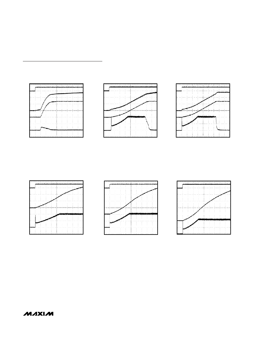
TURN-ON INTO CAPACITIVE LOAD
(C
L
= 0.47µF)
MAX5913A/14A toc10
0
A
B
0
C
0
D
0
400µs/div
RLYON = V
DD
A: V
ON
, 5V/div
B: V
GATE
, 20V/div
C: V
OUT
, 20V/div
D: I
OUT
, 100mA/div
TURN-ON INTO CAPACITIVE LOAD
(C
L
= 47µF)
MAX5913A/14A toc11
0
A
B
0
C
0
D
0
1ms/
div
RLYON = V
DD
, R
RTIM
= 2k
A: V
ON
, 5V/div
B: V
GATE
, 20V/div
C: V
OUT
, 20V/div
D: I
OUT
, 200mA/div
TURN-ON INTO CAPACITIVE LOAD
(C
L
= 470µF)
MAX5913A/14A toc12
0
A
B
0
C
0
D
0
10ms/div
RLYON = V
DD
, R
RTIM
= 40k
A: V
ON
, 5V/
div
B: V
GATE
, 20V/
div
C: V
OUT
, 20V/
div
D: I
OUT
, 200mA/
div
CURRENT-LIMIT FOLDBACK
(V
CC
= +36V)
MAX5913A/14A toc13
0
A
B
0
C
0
10ms/div
RLYON = V
DD
, R
L
= 100, R
RTIM
= 40k, C
LOAD
= 470µF
A: V
ON
, 5V/div
B: V
OUT
, 10V/div
C: I
OUT
, 200mA/div
CURRENT-LIMIT FOLDBACK
(V
CC
= +48V)
MAX5913A/14A toc14
0
A
B
0
C
0
10ms/div
RLYON = V
DD
, R
L
= 139, R
RTIM
= 40k, C
LOAD
= 470µF
A: V
ON
, 5V/div
B: V
OUT
, 10V/div
C: I
OUT
, 200mA/div
CURRENT-LIMIT FOLDBACK
(V
CC
= +57V)
MAX5913A/14A toc15
0
A
B
0
C
0
10ms/div
RLYON = V
DD
, R
L
= 162, R
RTIM
= 40k, C
LOAD
= 470µF
A: V
ON
, 5V/div
B: V
OUT
, 10V/div
C: I
OUT
, 200mA/div
Typical Operating Characteristics (continued)
(V
CSP
_ = V
CC
= +48V, V
DD
= +3.3V, V
RLY
= +12V, AGND = DGND = 0V, RTIM = open, T
A
= +25°C, unless otherwise specified.)