 | ÐлекÑÑоннÑй компоненÑ: XRT81L27 | СкаÑаÑÑ:  PDF PDF  ZIP ZIP |
/home/web/doc/html/exar/208074
Exar
Corporation 48720 Kato Road, Fremont CA, 94538
·
(510) 668-7000
·
FAX (510) 668-7017
·
www.exar.com
áç
áç
áç
áç
PRELIMINARY
XRT81L27
SEVEN CHANNEL E1 LINE INTERFACE UNIT WITH CLOCK RECOVERY
JULY 2001
REV. P1.0.3
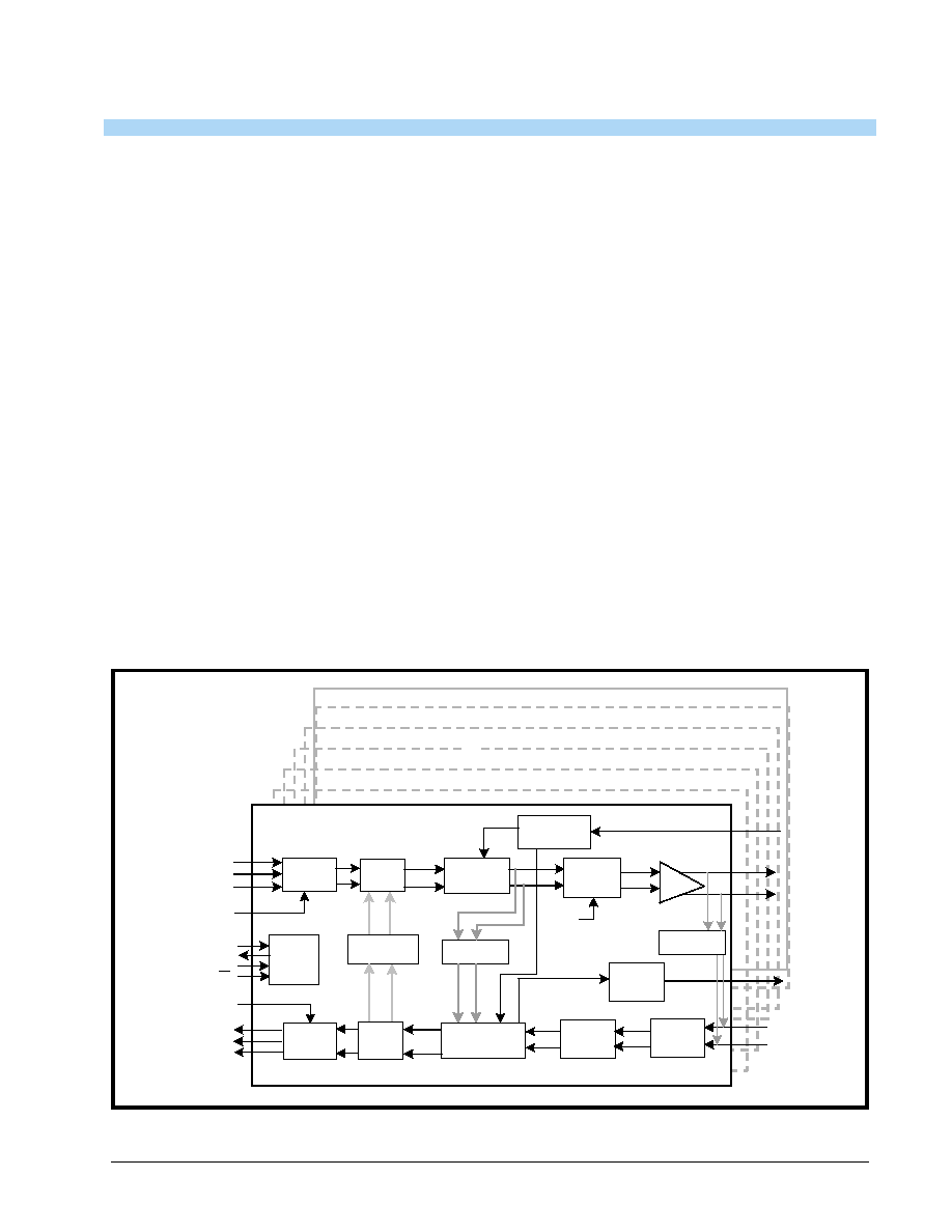
GENERAL DESCRIPTION
The XRT81L27 is an optimized seven-channel, ana-
log, 3.3V, line interface unit, fabricated using low
power CMOS technology. The device contains seven
independent E1 channels, including data and clock
recovery circuits. It is primarily targeted towards the
SDH multiplexers that accomodate TU12 Tributary
Unit Frames. Line cards in these units mutiplex 21 E1
channels into higher SDH rates. Devices with seven
E1 interfaces such as the XRT81L27 provide the
most efficient method of implementing 21-channel
line cards. Each channel performs the driver and re-
ceiver functions necessary to convert bipolar signals
to logical levels and vice versa.
The receiver input accepts transformer or capacitor
coupled signals, while the transmitter is coupled to
the line using a 1:2 step-up transformer. The same
transformer configuration can be used for both bal-
anced 120
and unbalanced 75
interfaces. The
Receiver Loss of Signal Detection is compliant to
G.775 and in Host Mode, the number of zeros re-
ceived before LOS is declared can be increased to
4096 bits. This feature provides the user with the
flexability to implement LOS specifications that re-
quire greater than G.775 requirements
FEATURES
· Consists of Seven (7) Independent E1 (CEPT) Line
Interface Units (Transmitter and Receiver)
· Generates Transmit Output Pulses that are Compli-
ant with the ITU-T G.703 Pulse Template Require-
ment for 2.048Mbps (E1) Rates
· On-Chip Pulse Shaping for both 75
and 120
line
drivers
· Receiver Can Either Be Transformer or Capacitive-
Coupled to the Line
· Detects and Clears LOS (Loss of Signal) Per ITU-T
G.775
· Compliant with the ITU-T G.823 Jitter Tolerance
Requirements
APPLICATIONS
· lPDH Multiplexers
· SDH Multiplexers
· Digital Cross-Connect Systems
· DECT (Digital European Cordless Telephone) Base
Stations
· CSU/DSU Equipment
F
IGURE
1. B
LOCK
D
IAGRAM
Channe
l 1
Channel 2
Channel 3
Channel 4
Channel 5
Channel 6
TAOS
Channel 7
Timing
Generator
MClk
Encoder
MUX
Timing
Control
TX Pulse
Shaper
TClk
TPOS/TDATA
TNEG/CODE
TTIP
TRing
Remote
Loopback
TClkP
Decoder
Data & Timing
Recovery
Peak
Detector
Receive
Equalizer
Line
Driver
RClk
RPOS
RClkP
RTIP
RRing
LOS
Detect
LOS
Local
Loopback
Serial
Processor
Interface
SDI
SDO
SClk
CS
MUX
Analog
Loopback
RNEG/LCV
XRT81L27
áç
áç
áç
áç
SEVEN CHANNEL E1 LINE INTERFACE UNIT WITH CLOCK RECOVERY
REV. P1.0.3
PRELIMINARY
2
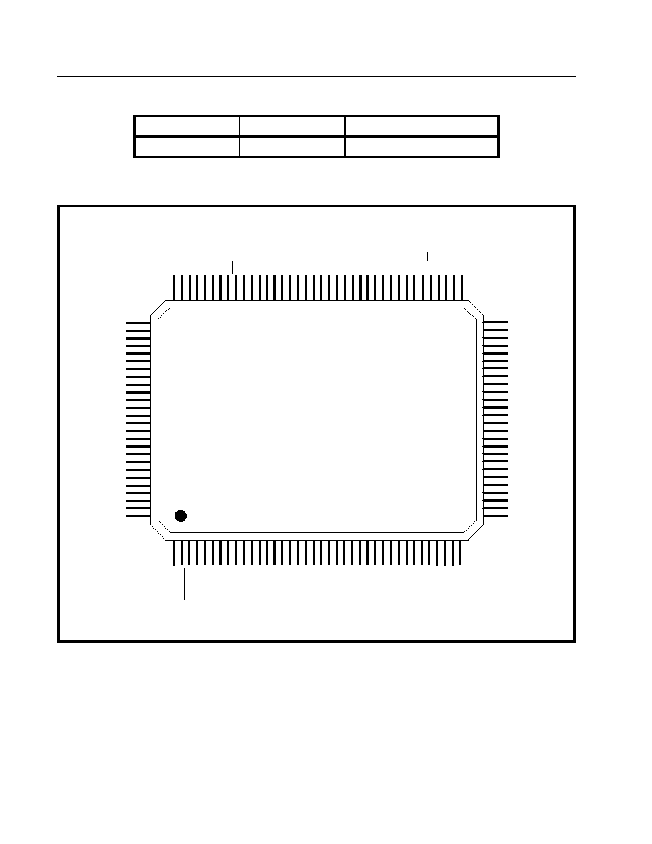
ORDERING INFORMATION
P
ART
N
O
.
P
ACKAGE
O
PERATING
T
EMPERATURE
R
ANGE
XRT81L27IV
128 Lead TQFP
-40°C to +85°C
F
IGURE
2. P
IN
O
UT
OF
THE
XRT81L27
XRT81L27
AVDD
AGND
TClk2
TPOS2/TDATA2
TNEG2/CODE
TAOS2
TClk4
TPOS4/TDATA4
TNEG4/CODE
TAOS4
TAOS3
TNEG3/CODE
TPOS3/TDATA3
TClk3
TAOS1
TNEG1/CODE
TPOS1/TDATA1
TClk1
GND
VDD
RPOS3/RData3
RNEG3/LCV3
RClk3
LOS3
RPOS1/RData1
RNEG1/LCV1
103
104
105
106
107
108
109
110
111
112
113
114
115
116
117
118
119
120
121
122
123
124
125
126
127
128
1
2
3
4
5
6
7
8
9
10
11
12
13
14
15
16
17
18
19
20
21
22
23
24
25
26
27
28
29
30
31
32
33
34
35
36
37
38
RClk1
LOS1
RST/LBEN
RTIP1
RRing1
PDTx1
TTIP1
TVDD1
TRing1
TGND1
PDTx3
TTIP3
TVDD3
TRing3
TGND3
AVDD
RTIP3
RRing3
AGND
RTIP5
RRing5
PDTx5
TTIP5
TVDD5
TRing5
TGND5
PDTx7
TTIP7
TVDD7
TRing7
TGND7
MODE
RClk5
RNEG5/LCV5
RPOS5/RDATA5
LOS5
TClk5
TPOS5/TDATA5
RPOS4/RDATA4
RNEG4/LCV4
RClk4
LOS4
RPOS2/RDATA2
RNEG2/LCV2
RClk2
LOS2
ICT
RTIP2
RRing2
PDTx2
TTIP2
TVDD2
TRing2
TGND2
PDTx4
TTIP4
TVDD4
TRing4
TGND4
AVDD
RTIP4
RRing4
AGND
RTIP6
RRing6
PDTx6
TTIP6
TVDD6
TRing6
TGND6
MCLK
SR/DR
RTIP7
RRing7
TClkP
RClkP
102
101
100
99
98
97
96
95
94
93
92
91
90
89
88
87
86
85
84
83
82
81
80
79
78
77
76
75
74
73
72
71
70
69
68
67
66
65
RClk7
RNEG7/LCV7
RPOS7/RData7
LOS7
RClk6
RNEG6/LCV6
RPOS6/RData6
LOS6
VDD
GND
TxClk6
TPOS6/TDATA6
TNEG6/CODE
TAOS6
CS/B3
SClk/B2
SDI/B1
SDO/LBM
TAOS7
TNEG7/CODE
TPOS7/TDATA7
TClk7
GND
VDD
TAOS5
TNEG5/CODE
64
63
62
61
60
59
58
57
56
55
54
53
52
51
50
49
48
47
46
45
44
43
42
41
40
39

áç
áç
áç
áç
XRT81L27
PRELIMINARY
SEVEN CHANNEL E1 LINE INTERFACE UNIT WITH CLOCK RECOVERY
REV. P1.0.3
I
TABLE OF CONTENTS
GENERAL DESCRIPTION .................................................................................................. 1
F
EATURES
................................................................................................................................................... 1
A
PPLICATIONS
.............................................................................................................................................. 1
Figure 1. Block Diagram ................................................................................................................................... 1
O
RDERING
I
NFORMATION
....................................................................................................................... 2
Figure 2. Pin Out of the XRT81L27 .................................................................................................................. 2
TABLE OF CONTENTS .................................................................................................................................... I
PIN DESCRIPTIONS ........................................................................................................... 3
T
ABLE
1: R
ECEIVER
E
LECTRICAL
C
HARACTERISTICS
.......................................................................................... 12
T
ABLE
2: T
RANSMITTER
E
LECTRICAL
C
HARACTERISTICS
.................................................................................... 13
Figure 3. Transmit Input Timing ...................................................................................................................... 13
Figure 4. Receive Output Timing .................................................................................................................... 14
T
ABLE
3: DC E
LECTRICAL
C
HARACTERISTICS
.................................................................................................... 14
1.0 The Microprocessor Serial Interface .............................................................................................. 15
1.1 D
ESCRIPTION
OF
THE
C
OMMAND
R
EGISTERS
.................................................................................................... 15
T
ABLE
4: M
ICROPROCESSOR
R
EGISTER
A
DDRESS
AND
C
ONTROL
...................................................................... 15
T
ABLE
5: R
EGISTER
C
ONTROL
B
IT
D
ESCRIPTION
............................................................................................... 16
Figure 5. Timing Diagram for the Microprocessor Serial Interface ................................................................. 18
M
ICROPROCESSOR
S
ERIAL
I
NTERFACE
T
IMING
(
SEE
F
IGURE
5) ................................................................... 18
Figure 6. Microprocessor Serial Interface Data Structure .............................................................................. 19
T
ABLE
6: AC E
LECTRICAL
C
HARACTERISTICS
.................................................................................................... 19
T
ABLE
7: P
ER
C
HANNEL
P
OWER
C
ONSUMPTION
INCLUDING
LINE
POWER
DISSIPATION
,
TRANSMISSION
AND
RECEIVE
PATHS
ALL
ACTIVE
.............................................................................................................................. 20
Figure 7. Illustration of the ITU-T G.703 Pulse Template for E1 Applications ................................................ 21
2.0 The Pulse Shaping Circuit ............................................................................................................... 21
2.1 I
NTERFACING
THE
T
RANSMIT
S
ECTIONS
OF
THE
XRT81L27
TO
THE
L
INE
.......................................................... 21
Figure 8. Illustration of how to interface the Transmit Sections of the XRT81L27 to the Line (for 75W Applica-
tions) ............................................................................................................................................. 22
Figure 9. Illustration of how to interface the Transmit Sections the XRT81L27 to the Line (for 120W Applications)
22
3.0 The Receive Section ........................................................................................................................ 23
3.1 I
NTERFACING
THE
R
ECEIVE
S
ECTIONS
TO
THE
L
INE
........................................................................................... 23
Figure 10. Recommended Schematic for Interfacing the Receive Sections of the XRT81L27 to the Line for 75W
Applications (Transformer-Coupling) ............................................................................................ 23
Figure 11. Recommended Schematic for Interfacing the Receive Sections of the XRT81L27 to the Line for 120W
Applications (Transformer-Coupling) ............................................................................................ 23
Figure 12. Recommended Schematic for Interfacing the Receive Sections of the XRT81L27 to the Line for 120W
Applications (Capacitive-Coupling) .............................................................................................. 24
3.2 T
HE
R
ECEIVE
E
QUALIZER
B
OCK
....................................................................................................................... 24
3.3 T
HE
P
EAK
D
ETECTOR
AND
S
LICER
B
LOCK
....................................................................................................... 24
3.4 T
HE
LOS D
ETECTOR
BLOCK
............................................................................................................................ 24
Figure 13. Package Outline Drawing .............................................................................................................. 25
R
EVISIONS
................................................................................................................................................. 26

XRT81L27
áç
áç
áç
áç
SEVEN CHANNEL E1 LINE INTERFACE UNIT WITH CLOCK RECOVERY
REV. P1.0.3
PRELIMINARY
3
PIN DESCRIPTIONS
P
IN
#
N
AME
T
YPE
D
ESCRIPTION
1
RClk1
O
Receiver 1 Clock Output
2
LOS1
O
Receiver 1 Loss of Signal:
This signal is asserted High to indicate loss of signal at the receive input.
3
RST/LBEN
I
Reset (Active-low):
In Host Mode, tie this pin "Low" to reset the serial register contents to zero.
Loop-back Enable (Active-low):
In Hardware Mode, when this pin is tied "Low", Loop-back mode is enabled.
N
OTES
:
1. See description of pin 47 to pin 50 for Local or Remote Loop-back
selection.
2. Internally pulled-high with 50K
.
4
RTIP1
I
Receiver 1 Bipolar Positive Input
5
RRing1
I
Receiver 1 Bipolar Negative Input
6
PDTx1
I
Powered-down Transmitter 1:
This pin is operational for both Host or Hardware mode, tie this pin High to
power-down channel 1 transmitter and set TTIP1 and TRing1 output to high
impedance.
N
OTE
: Internally pulled-high with 50K
.
7
TTIP1
O
Transmitter 1 Tip Output:
Positive bipolar data output to the line
8
TVDD1
****
Transmitter 1 Positive Supply (3.3V± 5%)
9
TRing1
O
Transmitter 1 Ring Output:
Negative bipolar data output to the line.
10
TGND1
****
Transmitter 1 Supply Ground
11
PDTx3
I
Powered-down Transmitter 3:
This pin is operational for both Host or Hardware mode, tie this pin High to
power-down channel 3 transmitter and set TTIP3 and TRing3 output to high
impedance.
N
OTE
: Internally pulled- high with 50K
.
12
TTIP3
O
Transmitter 3 Tip Output:
Positive bipolar data output to the line.
13
TVDD3
****
Transmitter 3 Positive Supply(3.3V± 5%)
14
TRing3
O
Transmitter 3 Ring Output:
Negative bipolar data output to the line.
15
TGND
****
Transmitter 3 Supply Ground
16
AVDD
****
Analog Positive Supply(3.3V± 5%)
17
RTIP3
I
Receiver 3 Bipolar Positive Input
18
RRing3
I
Receiver 3 Bipolar Negative Input
19
AGND
****
Analog Supply Ground
20
RTIP5
I
Receiver 5 Bipolar Positive Input

áç
áç
áç
áç
XRT81L27
SEVEN CHANNEL E1 LINE INTERFACE UNIT WITH CLOCK RECOVERY
PRELIMINARY
REV. P1.0.3
4
21
RRing5
I
Receiver 5 Bipolar Negative Input
22
PDTx5
I
Powered-down Transmitter 5:
This pin is operational for both Host or Hardware mode, tie this pin High to
power-down channel 5 transmitter and set TTIP5 and TRing5 output to high
impedance.
N
OTE
: Internally pulled- high with 50K
.
23
TTIP5
O
Transmitter 5 Tip Output:
Positive bipolar data output to the line.
24
TVDD5
****
Transmitter 5 Positive Supply(3.3V± 5%)
25
TRing5
O
Transmitter 5 Ring Output:
Negative bipolar data output to the line.
26
TGND5
****
Transmitter 5 Supply Ground
27
PDTx7
Powered-down Transmitter 7:
This pin is operational for both Host or Hardware mode, tie this pin High to
power-down channel 7 transmitter and set TTIP7 and TRing7 output to high
impedance.
N
OTE
: Internally pulled- high with 50K
.
28
TTIP7
O
Transmitter 7 Tip Output:
Positive bipolar data output to the line.
29
TVDD7
****
Transmitter 7 Positive Supply(3.3V± 5%)
30
TRing7
O
Transmitter 7 Ring Output:
Negative bipolar data output to the line.
31
TGND7
****
Transmitter 7 Supply Ground
32
MODE
I
Mode Control Input:
This pin is used for selecting Hardware Mode or Host Mode control of the
device. Left this pin unconnected or tie Low to select Host Mode and tie this
pin High to select Hardware mode.
N
OTE
: Internally pulled-down with 50K
.
33
RClk5
O
Receiver 5 Clock Output
34
RNEG5/LCV5
O
Receiver 5 Negative Data Output:
In dual-rail mode, this signal is the receive n-rail output data.
Line Code Violation Output:
In single-rail mode, this signal output High for one clock cycle to indicate a
code violation is detected in the received data. If AMI coding is selected,
every bipolar violation received will cause this pin to go High.
35
RPOS5/RDATA5
O
Receiver 5 Positive Data Output:
In dual-rail mode, this signal is the receive p-rail output data.
Receiver 5 NRZ Data Output:
In single-rail mode, this signal is the receive output data
36
LOS5
O
Receiver 5 Loss of Signal:
This signal is asserted High to indicate loss of signal at the receive input.
37
TClk5
I
Transmitter 5 Clock Input:
E1 rate at 2.048MHz ± 50ppm.
P
IN
#
N
AME
T
YPE
D
ESCRIPTION
Document Outline