
© 2005 California Micro Devices Corp. All rights reserved.
12/13/05
490 N. McCarthy Blvd., Milpitas, CA 95035-5112
Tel: 408.263.3214
Fax: 408.263.7846
www.cmd.com
1
CM1418
PRELIMINARY
Praetorian
TM L-C EMI Filter with ESD Protection
for Headset Speaker Applications
Features
∑
2 channels of EMI filtering
∑
±
30kV ESD protection
∑
(IEC 61000-4-2, contact discharge)
∑
±
30kV ESD protection (HBM)
∑
OptiGuard
TM
Coating for improved reliability at
assembly
∑
Greater than 35dB of attenuation at 1GHz
∑
6-bump, 1.720mm x 1.220mm footprint Chip Scale
Package (CSP)
∑
Lead-free version available
Applications
∑
Headset Speaker port in mobile handsets
∑
I/O port protection for mobile handsets, notebook
computers, PDAs etc.
∑
EMI filtering for data ports in cell phones, PDAs or
notebook computers.
Product Description
California Micro Devices' CM1418 is an L-C EMI filter
array with ESD protection, which integrates two Pi-
filters (C-L-C) for the headset speaker. The CM1418
has component values of 117pF-3.0nH-117pF. The
parts include ESD protection diodes on all input/output
pins, which provide a very high level of protection for
sensitive electronic components that may be subjected
to electrostatic discharge (ESD). The ESD diodes
connected to the filter ports safely dissipate ESD
strikes of
±
30kV, beyond the maximum requirement of
the IEC61000-4-2 international standard. Using the
MIL-STD-883 (Method 3015) specification for Human
Body Model (HBM) ESD, the pins are protected for
contact discharges at greater than
±
30kV.
This device is particularly well suited for portable
electronics (e.g. mobile handsets, PDAs, notebook
computers) because of its small package format and
easy-to-use pin assignments. In particular, the
CM1418 is ideal for EMI filtering and protecting
speaker output lines from ESD for the headset speaker
in mobile handsets. Most speakers have impedance of
8
and in order to maximize the power output, the
resistance of an EMI filter needs to be as low as
possible and the CM1418 addresses this by having a
C-L-C based EMI filter where the inductor has less
than 0.35
of resistance.
The CM1418 is available either uncoated or with Opti-
Guard
TM
coating resulting in improved reliability at
assembly. The CM1418 is also available in a space
saving, low profile Chip Scale Package with optional
lead-free finishing
.
Electrical Schematic
3nH
117pF
117pF
3nH
A3
B3
A1
B1
FILTER #1
FILTER #2
FILTER #2
FILTER #1
117pF
117pF
A2
GND
B2
GND
© 2005 California Micro Devices Corp. All rights reserved.
2
490 N. McCarthy Blvd., Milpitas, CA 95035-5112
Tel: 408.263.3214
Fax: 408.263.7846
www.cmd.com
12/13/05
CM1418
PRELIMINARY
Ordering Information
Note 1: Parts are shipped in Tape & Reel form unless otherwise specified.
Note 2: Lead-free devices are specified by using a "
+
" character for the top side orientation mark.
PIN DESCRIPTIONS
PIN
NAME
DESCRIPTION
A1
Filter #1
Filter #1 Input
A2
GND
Device Ground
A3
Filter #1
Filter #1 Input
B1
Filter #2
Filter #2 Input
B2
GND
Device Ground
B3
Filter #2
Filter #2 Input
XX
3
2
1
B
A
Orientation
Marking
(see note 2)
A3
B3
A2
A1
B2
B1
A1
Orientation
Marking
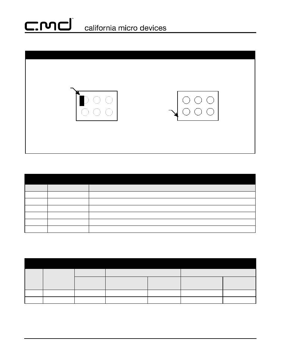
PACKAGE / PINOUT DIAGRAMS
Notes:
CM1418
CSP Package
TOP VIEW
BOTTOM VIEW
(Bumps Down View)
(Bumps Up View)
2)
Lead-free devices are specified by using a "+" character for the top side orientation mark.
1)
These drawings are not to scale.
PART NUMBERING INFORMATION
Pins
Package
Standard Finish
Lead-free Finish
2
OptiGuard
TM
Coating
Ordering Part
Number
1
Part Marking
Ordering Part
Number
1
Part Marking
6
CSP
Y
CM1418-02CS
CG
CM1418-02CP
CG
6
CSP
N
CM1418-0BCS
AL
CM1418-0BCP
AL

© 2005 California Micro Devices Corp. All rights reserved.
12/13/05
490 N. McCarthy Blvd., Milpitas, CA 95035-5112
Tel: 408.263.3214
Fax: 408.263.7846
www.cmd.com
3
CM1418
PRELIMINARY
Specifications
Note 1: T
A
=25
∞
C unless otherwise specified.
Note 2: ESD applied to input and output pins with respect to GND, one at a time.
Note 3: These parameters are guaranteed by design and characterization.
ABSOLUTE MAXIMUM RATINGS
PARAMETER
RATING
UNITS
Storage Temperature Range
-65 to +150
∞C
DC Current per Inductor
30
mA
DC Package Power Rating
0.5
W
STANDARD OPERATING CONDITIONS
PARAMETER
RATING
UNITS
Operating Temperature Range
-40 to +85
∞C
ELECTRICAL OPERATING CHARACTERISTICS
(SEE NOTE 1)
SYMBOL
PARAMETER
CONDITIONS
MIN
TYP
MAX
UNITS
L
Inductance
3.0
nH
R
DC Channel Resistance
0.28
0.35
C
TOT
Total Channel Capacitance
2.5V dc; 1MHz, 30mV ac
187
234
281
pF
C
1
Capacitance C
1
2.5V dc; 1MHz, 30mV ac
93
117
140
pF
V
ST
Stand-off Voltage
I
= 10
A
6.0
V
I
LEAK
Diode Leakage Current
V
IN
=
±
3.3V
0.1
1.0
A
V
SIG
Signal Clamp Voltage
Positive Clamp
Negative Clamp
I
LOAD
= 10mA
I
LOAD
= -10mA
5.6
-9.0
6.8
-6.8
9.0
-5.6
V
V
V
ESD
In-system ESD Withstand Voltage
a) Human Body Model, MIL-STD-883,
Method 3015
b) Contact Discharge per IEC 61000-4-2
Level 4
Notes 2 and 3
±30
±30
kV
kV
R
DYN
Dynamic Resistance
Positive
Negative
0.95
0.90
f
C
Cut-off frequency
Z
SOURCE
= 50
, Z
LOAD
= 50
L = 3nH, C = 117pF
22
MHz

© 2005 California Micro Devices Corp. All rights reserved.
4
490 N. McCarthy Blvd., Milpitas, CA 95035-5112
Tel: 408.263.3214
Fax: 408.263.7846
www.cmd.com
12/13/05
CM1418
PRELIMINARY
Performance Information
Typical Filter Performance (nominal conditions unless specified otherwise, 50 Ohm Environment)
Figure 1. Insertion Loss vs. Frequency (Filter #1 to GND B2)
Figure 2. Insertion Loss vs. Frequency (Filter #2 to GND B2)
To be determined
