
August 2004
ASM5CVF857
rev 1.2
2.5V Wide-Range Frequency Clock Driver (60 MHz
≠ 200 MHz)
1 of 15
Notice: The information in this document is subject to change without notice.
2.5V Wide-Range Frequency Clock Driver (60MHz
≠ 200MHz)
Features
∑
Low skew; low jitter PLL clock driver.
∑
1 to 10 differential clock distribution (SSTL_2).
∑
Feedback pins for input to output synchronization.
∑
PDB for power management.
∑
Spread spectrum tolerant inputs.
∑
Auto-PD when input signal removed.
∑
Choice of static phase offset for easy board tuning:
∑ -XXX = device pattern number for options listed
below:
∑ PCV857-025 - 0 ps
∑ PCV857-1300 - +50 ps
Product Description
This PLL clock buffer is designed for a V
DD
of 2.5V,
AV
DD
of 2.5V and differential data input a
nd output
levels.
ASM5CVF857 is a zero-delay buffer that
distributes a differential clock input pair (CLK_INT,
CLK_INC) to ten differential pairs of clock outputs
(CLKT[0:9], CLKC[0:9]) and one differential pair
feedback clock output (FB_OUT, FB_OUTC). The clock
outputs are controlled by the input clocks (CLK_INT,
CLKINC), the feedback clocks (FB_INT, FB_INC), the
2,5V LVCMOS input (PDB), and the analog power input
(AV
DD
). When input (PDB) is low while power is applied,
the receivers are disabled, the PLL is turned off, and
the differential clock outputs are tri-stated. When AV
DD
is grounded, the PLL is turned off and bypassed for test
purposes.
When the input frequency is less than the operating
frequency of the PLL, approximately 20MHz, the device
will enter a low power mode. An input frequency
detection circuit on the differential inputs, independent
from the input buffers, will detect the low frequency
condition and perform the same low power features as
and when the PDB input is low. When the input
frequency increases to greater than approximately
20MHz, the PLL will be turned back on, the inputs and
outputs will be enabled, and the PLL will obtain phase
lock between the feedback clock pair (FB_INT,
FB_INC) and the input clock pair (CLK_INT, CLK_INC).
The PLL in the ASM5CVF857 clock driver uses the
input clocks (CLK_INT, CLKINC) and the feedback
clocks (FB_INT, FB_INC) to provide high-performance,
low-skew, low-jitter output differential clocks (CLKT[0:9],
CLKC[0:9]). ASM5CVF857 is also able to track spread
spectrum clock (SSC) for reduced EMI.
ASM5CVF857 is characterized for operation from 0∞C
to 85∞C.
Applications
∑
DDR Memory Modules / Zero Delay Board Fan
Out.
∑
Provides complete DDR DIMM logic solution with
ASM4SSTVF16857, ASM4SSTVF16859 &
ASM4SSTVF32852.
Specifications
∑
Meets PC3200 specification for DDR-I 400 support.
∑
Covers all DDRI speed grades.
Switching Characteristics
∑
CYCLE-CYCLE jitter : <50ps.
∑
OUT-OUTPUT skew: <40ps.
∑
Period jitter: ±30ps.

August 2004
ASM5CVF857
rev 1.2
2.5V Wide-Range Frequency Clock Driver (60 MHz
≠ 200 MHz)
2 of 15
Notice: The information in this document is subject to change without notice.
F B_O UTT
F B_O UTC
CLKT0
CLKC0
CLKT1
CLKC1
CLKT2
CLKC2
CLKT3
CLKC3
CLKT4
CLKC4
CLKT5
CLKC5
CLKT6
CLKC6
CLKT7
CLKC7
CLKT8
CLKC8
CLKT9
C L KC 9
Control
PLL
AVDD
PDB
FB_INT
FB_INC
CLK_INC
CLK_INT
Logic
1
2
3
4
5
6
7
8
9
10
11
12
13
14
15
16
17
18
19
20
21
22
23
24
25
26
27
28
29
30
31
32
33
34
35
36
37
38
39
40
41
42
43
44
45
46
47
48
GND
CLKC0
CLKT0
VDD
CLKT1
CLKC1
GND
GND
CLKC2
CLKT2
VDD
VDD
CLK_IN T
CLK_INC
VDD
AVDD
AGND
GND
CLKC3
CLKT3
VDD
CLKT4
CLKC4
GND
GND
CLKC5
CLKT5
VDD
CLKT6
CLKC6
GND
GND
CLKC7
CLKT7
VDD
PDB
FB_INT
FB_INC
VDD
FB_OUT C
FB_OUT T
GND
CLKC8
CLKT8
VDD
CLKT9
CLKC9
GND
A
S
M
5
C
V
F
8
5
7
Block Diagram
Pin Configuration

August 2004
ASM5CVF857
rev 1.2
2.5V Wide-Range Frequency Clock Driver (60 MHz
≠ 200 MHz)
3 of 15
Notice: The information in this document is subject to change without notice.
56-BALL BGA
1
2
3
4
5
6
A
CLKT0
CLKC0
GND
GND
CLKC5
CLKT5
B
CLKC1
CLKT1
VDD
VDD
CLKT6
CLKC6
C
GND
GND
NC
NC
GND
GND
D
CLKT2
CLKC2
NC
NC
CLKC7
CLKC7
E
VDD
VDD
NB
NB
VDD
PDB
F
CLK_INT
CLK_INC
NB
NB
FB_INC
FB_INT
G
VDD
AVDD
NC
NC
FB_OUTC
VDD
H
AGND
GND
NC
NC
GND
FB_OUTT
J
CLKC3
CLKT3
VDD
VDD
CLKT8
CLKC8
K
CLKT4
CLKC4
GND
GND
CLKC9
CLKT9
A
E
F
G
H
J
B
C
D
K
1
2
3
4
5
6
56-BALL BGA
(SEE TABLE BELOW)
C
L
K
T
3
V
D
D
C
L
K
T
4
C
L
K
C
4
C
L
K
C
9
C
L
K
T
9
C
L
K
C
3
C
L
K
C
8
C
L
K
T
8
V
D
D
C
L
K
T
1
V
D
D
C
L
K
T
0
C
L
K
C
0
C
L
K
C
5
C
L
K
T
5
C
L
K
C
1
C
L
K
C
6
C
L
K
T
6
V
D
D
GND
CLKC2
CLKT2
CLK_IN
VDD
VDD
CLK_INC
AVDD
AGND
GND
CLKC7
CLKT7
VDD
FB_INT
PDB
VDD
FB_INC
VDD
FB_OUTC
FB_OUTT
ASM5CVF857
40-PIN MLF

August 2004
ASM5CVF857
rev 1.2
2.5V Wide-Range Frequency Clock Driver (60 MHz
≠ 200 MHz)
4 of 15
Notice: The information in this document is subject to change without notice.
Pin Description
Pin Number
Pin Name
Pin
Type
Pin Description
4, 11, 12, 15, 21, 28, 34, 38, 45
VDD
P
Power supply, 2.5V
1, 7, 8, 18, 24, 25, 31, 41, 42, 48
GND
P
Ground.
16
AVDD
P
Analog power supply, 2.5V.
17
AGND
P
Analog ground.
27, 29, 39, 44, 46, 22, 20, 10, 5, 3
CLKT(9:0)
O
"True" clock of differential pair outputs.
26, 30, 40, 43, 47, 23, 19, 9, 6, 2
CLKC(9:0)
O
"Complementary" clocks of differential pair outputs.
14
CLK_INC
I
"Complementary" reference clock input.
13
CLK_INT
I
"True" reference clock input.
33
FB_OUTC
O
"Complementary" feedback output dedicated for external
feedback. It switches at the same frequency as the CLK. This
output must be wired to FB_INC.
32
FB_OUTT
O
"True" feedback output dedicated for external feedback. It
switches at the same frequency as the CLK. This output must be
wired to FB_INT.
36
FB_INT
I
"True" feedback input provides feedback signal to the internal
PLL for synchronization with CLK_INT to eliminate phase error.
35
FB_INC
I
"Complementary" feedback input provides signal to the internal
PLL for synchronization with CLK_INC to eliminate phase error.
37
PDB
I
Power down. LVCMOS input.

August 2004
ASM5CVF857
rev 1.2
2.5V Wide-Range Frequency Clock Driver (60 MHz
≠ 200 MHz)
5 of 15
Notice: The information in this document is subject to change without notice.
Functionality
Inputs
Outputs
PLL State
AVDD
PDB
CLK_INT
CLK_INC
CLKT
CLKC
FB_OUTT
FB_OUTC
GND
H
L
H
L
H
L
H
Bypassed/Off
GND
H
H
L
H
L
H
L
Bypassed/Off
2.5V (nom)
L
L
H
Z
Z
Z
Z
off
2.5V (nom)
L
H
L
Z
Z
Z
Z
off
2.5V (nom)
H
L
H
L
H
L
H
on
2.5V (nom)
H
H
L
H
L
H
L
on
2.5V (nom)
X
<20 MHz
Z
Z
Z
Z
off
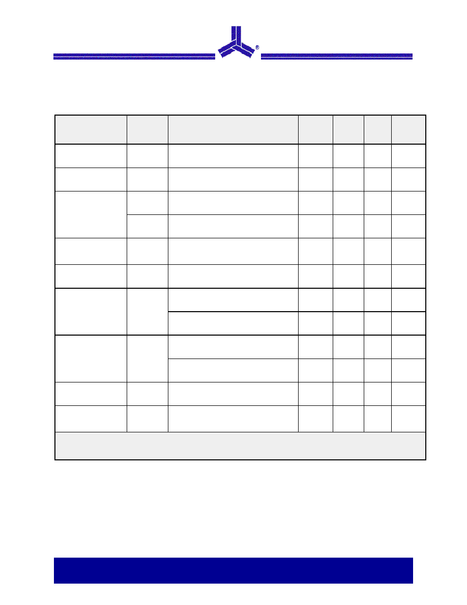
Absolute Maximum Ratings
Parameter
Min
Max
Unit
Supply voltage (VDD and AVDD)
-0.5
3.6
V
Logic Inputs
GND - 0.5
VDD + 0.5
V
Ambient Operating Temperature
0
85
˚C
Storage Temperature
-65
150
˚C
These are stress ratings only and functional operation is not implied. Exposure to absolute maximum ratings for
prolonged periods may affect device reliability.
August 2004
ASM5CVF857
rev 1.2
2.5V Wide-Range Frequency Clock Driver (60 MHz
≠ 200 MHz)
6 of 15
Notice: The information in this document is subject to change without notice.
Electrical Characteristics - Input/Supply/Common Output Parameters
T
A
= 0∞76C to 85∞C. Supply voltage AV
DD
and V
DD
=2.5V ± 0.2V (unless otherwise stated).
Parameter
Symbol
Conditions
Min
Typ
Max
Units
Input high current
I
IH
V
I
= V
DD
or GND
5
µA
Input low current
I
IL
V
I
= V
DD
or GND
5
µA
I
DDQ
C
L
= 0pF, R
L
= 120
, F
CLK_IN
= 200MHz
310
mA
Operating supply
current
I
DDPD
PDB = GND, FCLK_IN=0MHz
100
200
µA
Supply Current on
AVDD
I
ADD
F
CLK_IN
= 200MHz
9
12
mA
Input clamp voltage
V
IK
V
DDQ
=2.3V I
IN
= -18mA
-1.2
V
I
OH
= -100µA
V
DD
-0.1
V
High-level output
voltage
V
OH
I
OH
= -12mA
1.7
V
I
OL
= 100µA
0.1
V
Low-level output
voltage
V
OL
I
OL
= 12mA
0.6
V
Input capacitance*
C
IN
V
I
= GND or V
DD
2
3.5
pF
Input capacitance
variation
C
I(
V
OUT
= GND or V
DD
-0.25
0.25
pF
* Guaranteed by design at 200MHz; not 100% tested in production.

August 2004
ASM5CVF857
rev 1.2
2.5V Wide-Range Frequency Clock Driver (60 MHz
≠ 200 MHz)
7 of 15
Notice: The information in this document is subject to change without notice.
Recommended Operating Conditions
T
A
= 0∞C to 85∞C. Supply voltage AV
DD
and V
DD
=2.5V ± 0.2V (unless otherwise stated).
Parameter**
Symbol
Conditions
Min
Typ
Max
Unit
Supply Voltage
V
DD
, A
VDD
2.3
2.5
2.7
V
Low level input
voltage
V
IL
CLK_INT, CLK_INC, FB_INT,
FB_INC
0.4
V
DD
/2 - 0.18
V
V
IH
CLK_INT, CLK_INC, FB_INT,
FB_INC
V
DD
/2 + 0.18
2.1
V
High level input
voltage
PDB
1.7
V
DD
+ 0.3
V
DC input signal
voltage
#
V
IN
-0.3
V
DD
+ 0.3
V
V
ID
DC: CLK_INT, CLK_INC, FB_INT,
FB_INC
0.36
V
DD
+ 0.6
V
Differential input
signal voltage
$
AC: CLK_INT, CLK_INC, FB_INT,
FB_INC
0.7
V
DD
+ 0.6
V
Output differential
cross voltage
@
V
OX
V
DD
/2 - 0.15
V
DD
/2 + 0.15
V
Input differential
cross voltage
V
IX
V
DD
/2 - 0.2
V
DD
/2 + 0.2
V
High-level output
current
I
OH
-12
mA
Low-level output
current
I
OL
12
mA
Operating free-air
temperature
T
A
0
85
∞C
**: Unused inputs must be held high or low to prevent them from floating.
#: DC input signal voltage specifies the allowable DC execution of differential
$: Differential inputs signal voltages specify the differential voltage [VTR-VCP] required for switching where VTR is the true input
level and VCT is the complementary input level.
@: Differential cross-point voltage is expected to track variations of V
DD
and is the voltage at which the differential signal must be
crossing.

August 2004
ASM5CVF857
rev 1.2
2.5V Wide-Range Frequency Clock Driver (60 MHz
≠ 200 MHz)
8 of 15
Notice: The information in this document is subject to change without notice.
Timing Requirements**
Parameter
Symbol
Conditions
Min
Max
Units
Operating clock frequency
freq
op
2.5V ± 0.2V
60
220
MHz
Application Frequency Range
freq
app
2.5V ± 0.2V
95
220
MHz
Input clock duty cycle
d
tin
40
60
%
CLK stabilization
T
STAB
100
µs

August 2004
ASM5CVF857
rev 1.2
2.5V Wide-Range Frequency Clock Driver (60 MHz
≠ 200 MHz)
9 of 15
Notice: The information in this document is subject to change without notice.
Switching Characteristics**
Parameter
Symbol
Conditions
Min
Typ
Max
Units
Low-to-high level propagation delay time
t
PLH
*
CLK_IN to any output
3.5
ns
High-to-low level propagation delay time
t
PHL
*
CLK_IN to any output
3.5
ns
Output enable time
t
en
PDB to any output
3
ns
Output disable time
t
dis
PDB to any output
3
ns
Period Jitter
t
jit(per)
100MHz to 200MHz
-30
30
ps
Half-period jitter
t
jit(hper)
100MHz to 200MHz
-75
75
ps
Input clock slew rate
t
sl(I)
1
4
v/ns
Output clock slew rate
t
sl(o)
100/133/167/200 MHz
1
2
v/ns
Cycle-to-cycle jitter
t
cyc
-t
cyc
100 MHz to 200MHz
-50
50
ps
Static phase offset
t
(phase error)
#
-50
0
50
ps
Output-to-output skew
t
skew
40
60
ps
The PLL on the ASM5CVF857 is capable of meeting all the above parameters while supporting SSC synthesizers with
the following parameters.
SSC modulation frequency
30.00
50.00
kHz
SSC clock input frequency deviation
0.00
-0.50
%
PLL loop bandwidth
2
MHz
Phase angle
-0.031
∞
*: Refers to transition on non-inverting output in PLL bypass mode.
#: Static phase offset does not include jitter.
** T
A
= 0
˚ 85˙C. Supply voltage AV
DD
, V
DD
=2.5V ± 0.2V (unless otherwise stated).
Note: While the pulse skew is almost constant over frequency, the duty cycle error increases at higher frequencies. This
is due to the formula: duty cycle = t
WH
/tC where the cycle (t
C
) decreases as the frequency goes up.
Note: Switching characteristics guaranteed for application frequency range.

August 2004
ASM5CVF857
rev 1.2
2.5V Wide-Range Frequency Clock Driver (60 MHz
≠ 200 MHz)
10 of 15
Notice: The information in this document is subject to change without notice.
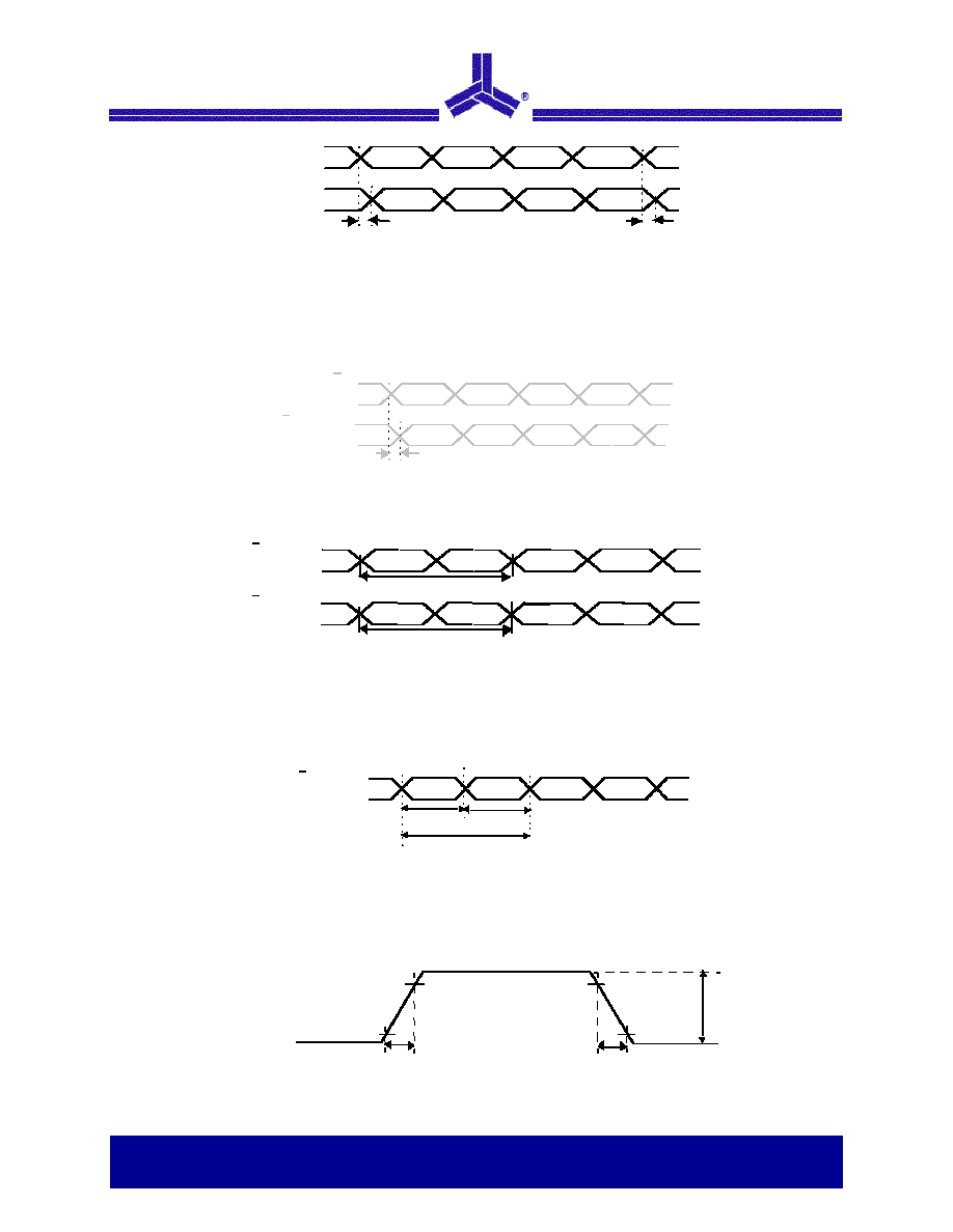
V
DD
V
( C L K T )
R = 60
V
DD
/2
ASM5CVF857
GND
V
( C L K C )
R = 60
Figure 1: IBIS Model Output Load
V
DD
/2
Z=50
R = 10
SCOPE
Z=60
Z=60
Z=50
C = 14 pF
R = 10
R = 50
R = 50
-V
DD
/2
-V
DD
/2
-V
DD
/2
ASM5CVF857
C = 14 pF
V
TT
V
TT
Note: V
TT
= GND
Figure 2: Output Load Test Circuit
V
DD
Z=120
SCOPE
Z=60
Z=60
C = 14 pF
R = 1 M
GND
GND
GND
ASM5CVF857
C = 14 pF
V
TT
V
TT
Note: V
TT
= GND
C = 1 pF
C = 1 pF
R = 1 M
Figure 3: Output Load Test Circuit for Crossing Point
t
c(n)
t
c(n+1)
t
jit(cc)
= t
c(n)
± t
c(n+1)
Y
X
, FB_OUTC
Y
X
, FB_OUTT
Figure 4: Cycle-to-Cycle Jitter Period
Parameter Measurement Information
August 2004
ASM5CVF857
rev 1.2
2.5V Wide-Range Frequency Clock Driver (60 MHz
≠ 200 MHz)
11 of 15
Notice: The information in this document is subject to change without notice.
Y
X
, FB_OUTC
Y
X
, FB_OUTT
Y
X
Y
X
t
(skew)
Figure 6: Output Skew
t
half period n
t
half period n+1
f
o
= average input frequency measured at CLK_INT/CLK_INC
n = any half cycle
Figure 8: Half-Period Jitter
Y
X
, FB_OUTC
Y
X
, FB_OUTT
Y , FB_OUTC
Y
Y
Y
t
c(n)
f
o
= average input frequency measured at CLK_INT/CLK_INC
Figure 7: Period Jitter
X
X
, FB_OUTC
X
, FB_OUTT
X
, FB_OUTT
CLK_INC
CLK_INT
FB_INC
FB_INT
(N > 1000 samples)
t
(
n+1
t
(
n
Figure 5: Static Phase Offset
80%
Clock inputs and outputs
Figure 9: Input and Output Slew rates
20%
V
ID
,V
OD
t
r(i)
, t
r(o)
t
f(i)
, t
f(o)
80%
20%

August 2004
ASM5CVF857
rev 1.2
2.5V Wide-Range Frequency Clock Driver (60 MHz
≠ 200 MHz)
12 of 15
Notice: The information in this document is subject to change without notice.
Package Dimensions (
6.10mm (240 mil) body, 0.50mm (0.020 mil) pitch TSSOP)
Dimensions (mm)
Dimensions (inches)
Symbol
Min
Max
Min
Max
A
-
1.20
-
0.047
A1
0.05
0.15
0.002
0.006
A2
0.80
1.05
0.32
0.041
b
0.17
0.27
0.007
0.011
c
0.09
0.20
0.0035
0.008
D
See Variations
E
8.10 Basic
0.319 Basic
E1
6.00
6.20
0.236
0.244
e
0.50 Basic
0.20 Basic
L
0.45
0.75
0.018
0.030
N
See Variations
0∞
8∞
0∞
8∞
aaa
-
0.10
-
0.004
C
1 2
N
E1
E
D
Index Area
L
A
A1
A2
e
b
aaa
C
D
Seating Plane
D (MM)
D(inch)
Min
Max
Min
Max
48
12.40
12.60
0.488
0.496

August 2004
ASM5CVF857
rev 1.2
2.5V Wide-Range Frequency Clock Driver (60 MHz
≠ 200 MHz)
13 of 15
Notice: The information in this document is subject to change without notice.
1 2
N
E1
E
D
Index Area
C
L
A
A1
A2
e
b
aaa
C
D
Seating Plane
Package Dimensions (4.40mm (1713 mil) body, 0.40 mm (16 mil) pitch TVSOP)
Dimensions (mm)
Dimensions (inches)
Symbol
Min
Max
Min
Max
A
-
1.20
-
0.047
A1
0.05
0.15
0.002
0.006
A2
0.80
1.05
0.32
0.041
b
0.17
0.27
0.007
0.011
c
0.09
0.20
0.0035
0.008
D
See Variations
E
8.10 Basic
0.319 Basic
E1
6.00
6.20
0.236
0.244
e
0.50 Basic
0.20 Basic
L
0.45
0.75
0.018
0.030
N
See Variations
0∞
8∞
0∞
8∞
aaa
-
0.10
-
0.004
D (MM)
D(inch)
N
Min
Max
Min
Max
48
12.40
12.60
0.488
0.496

August 2004
ASM5CVF857
rev 1.2
2.5V Wide-Range Frequency Clock Driver (60 MHz
≠ 200 MHz)
14 of 15
Notice: The information in this document is subject to change without notice.
Ordering Codes
Ordering Number
Marking
Package Type
Quantity Per Reel
Temperature
ASM5CVF857-48TT
AS5CVF857T
48-pin TSSOP, tube
0∞C to 70∞C
ASM5CVF857-48TR
AS5CVF857T
48-pin TSSOP, tape & reel
2500
0∞C to 70∞C
ASM5CVF857-48VT
AS5CVF857V
48-pin TVSOP, tube
0∞C to 70∞C
ASM5CVF857-48VR
AS5CVF857V
48-pin TVSOP, tape & reel
2500
0∞C to 70∞C
ASM5CVF857-56BT
AS5CVF857B
56-pin Ball BGA, tube
0∞C to 70∞C
ASM5CVF857-56BR
AS5CVF857B
56-pin Ball BGA, tape & reel
2500
0∞C to 70∞C
ASM5CVF857-40QT
AS5CVF857M
40-pin QFN, tube
0∞C to 70∞C
ASM5CVF857-40QR
AS5CVF857M
40-pin QFN, tape & reel
2500
0∞C to 70∞C
August 2004
ASM5CVF857
rev 1.2
2.5V Wide-Range Frequency Clock Driver (60 MHz
≠ 200 MHz)
15 of 15
Notice: The information in this document is subject to change without notice.
© Copyright 2003 Alliance Semiconductor Corporation. All rights reserved. Our three-point logo, our name and
Intelliwatt are trademarks or registered trademarks of Alliance. All other brand and product names may be the
trademarks of their respective companies. Alliance reserves the right to make changes to this document and its
products at any time without notice. Alliance assumes no responsibility for any errors that may appear in this
document. The data contained herein represents Alliance's best data and/or estimates at the time of issuance.
Alliance reserves the right to change or correct this data at any time, without notice. If the product described herein is
under development, significant changes to these specifications are possible. The information in this product data
sheet is intended to be general descriptive information for potential customers and users, and is not intended to
operate as, or provide, any guarantee or warrantee to any user or customer. Alliance does not assume any
responsibility or liability arising out of the application or use of any product described herein, and disclaims any
express or implied warranties related to the sale and/or use of Alliance products including liability or warranties
related to fitness for a particular purpose, merchantability, or infringement of any intellectual property rights, except as
express agreed to in Alliance's Terms and Conditions of Sale (which are available from Alliance). All sales of Alliance
products are made exclusively according to Alliance's Terms and Conditions of Sale. The purchase of products from
Alliance does not convey a license under any patent rights, copyrights; mask works rights, trademarks, or any other
intellectual property rights of Alliance or third parties. Alliance does not authorize its products for use as critical
components in life-supporting systems where a malfunction or failure may reasonably be expected to result in
significant injury to the user, and the inclusion of Alliance products in such life-supporting systems implies that the
manufacturer assumes all risk of such use and agrees to indemnify Alliance against all claims arising from such use.
Alliance Semiconductor Corporation
2595, Augustine Drive,
Santa Clara, CA 95054
Tel# 408-855-4900
Fax: 408-855-4999
www.alsc.com
Copyright ˇ Alliance Semiconductor
All Rights Reserved
Advance Information
Part Number: ASM5CVF857
Document Version: v1.1