Hfct5402D.p65
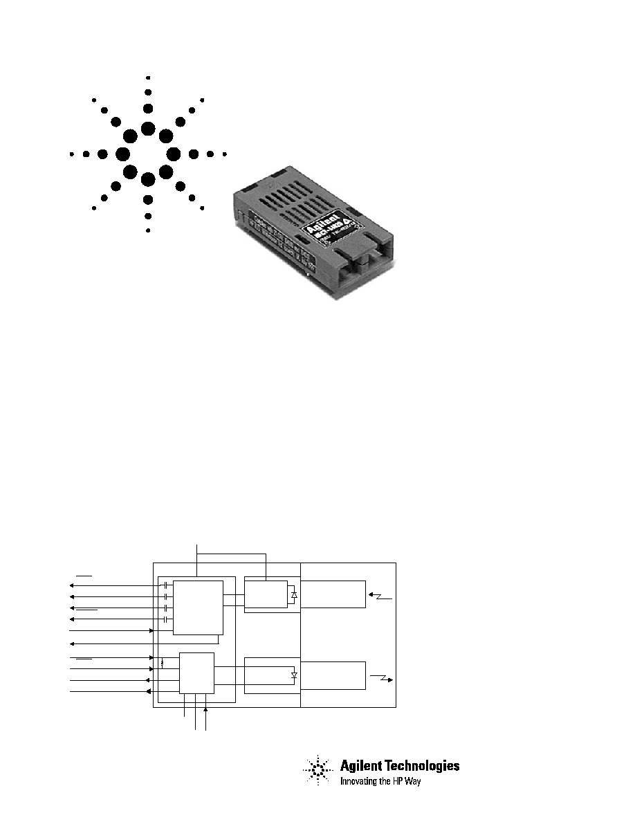
Agilent HFCT-5402D 2488 Mb/s
Single Mode Fiber Transceiver for
SONET OC-48/SDH STM-16 and ATM
Data Sheet
Description
General
The HFCT-5402D is a 1300 nm
laser-based duplex SC receptacle
2 x 9 transceiver with integral
clock and data recovery circuits.
It provides a cost-effective
solution for short haul 2488 Mb/s
data link requirements.
This compact transceiver requires
a single +5 V source and contains
the following features as depicted
in Figure 1: differential data input,
differential retimed data output,
differential recovered clock
output, laser bias monitor, signal
detect and transmitter disable.
Transmitter Section
The transmitter section of the
HFCT-5402D is similar to 1300 nm
single mode transceivers in use at
the 155 and 622 Mb/s rate. It
consists of a 1300 nm InGaAsP
laser in an eye-safe optical
subassembly (OSA) which mates
to the fiber cable. The laser OSA
is driven by a custom, silicon
bipolar IC which converts
differential input PECL logic
signal into an analog laser drive
current.
Features
· 1300 nm single mode transceiver
for SONET/SDH short reach links
· Compliant with proposed ATM
Forum 2488 Mb/s physical layer
specification
· Compliant with SONET jitter
tolerance and generation
specifications
· Integral duplex SC connector
receptacle compliant with
TIA/EIA and IEC standards
· Incorporates Agilent's eye safe
laser subassembly
· Single +5 V power supply
operation
· Integral PLL based clock recovery
circuit provides regenerated
differential clock and data
outputs (CML)
· Transmitter disable function
· Temperature range: 0°C - +70°C
· Wave solder and aqueous wash
process compatible
· Manufactured in an ISO 9001
certified facility
Applications
· ATM 2488 Mb/s links
· SONET OC-48/SDH STM-16
interconnections
Figure 1. Block Diagram
ELECTRICAL SUBASSEMBLY
DATA
CLOCK
SIGNAL DETECT
CLOCK & DATA
RECOVERY
AND POST
AMPLIFIER IC
LASER
DRIVER
IC
PRE-
AMPLIFIER
IC
LASER
PIN PHOTODIODE
DUPLEX SC
RECEPTACLE
TOP VIEW
CLOCK
DATA
TRANSMIT
DISABLE
LASER BIAS MONITOR +
DATA
+V
CCT
REF CLK
DATA
+V
CCR
100 nF
1 nF
LASER BIAS MONITOR -
100
W
V
EE
2
Receiver Section
The receiver section of the
transceiver provides a full set of
features including an integral
clock and data recovery (CDR)
circuit together with signal detect
function.
The receiver utilizes an InGaAs
PIN photodiode mounted together
with a transimpedance
preamplifier IC. This is connected
to custom silicon circuits
providing post-amplification and
quantization, CDR function and
signal detection.
CDR Function
In normal operation, the CDR data
loop is able to acquire and
maintain bit lock with the use of
the external reference clock. The
recovered clock is used to re-time
the quantizer data output, which
completes the full CDR function.
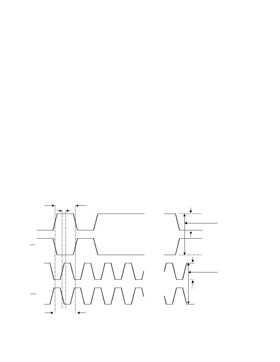
The relative timing relationship
between the output retimed data
and the recovered clock signals is
shown graphically in Figure 2. The
voltage swing measurement
method is also shown for clock
and data outputs.
For input optical power greater
than the specified receiver
sensitivity of -18.5 dBm, the
bit-error-ratio will be better than
1 x 10
-10
. The SD (signal detect)
will be deasserted when loss of
optical signal occurs.
Reference Clock
With `intermittent' or `no data
condition' the output clock will
slowly drift away from the
2.48832 GHz. The reference clock
enables the VCXO to acquire and
maintain lock. Ref Clk input is self
biasing and 50
W input terminated.
Temperature Range
The HFCT-5402D is specified for
operation over normal commercial
temperature range of 0° to +70°C
with recommended metal shield in
place (see Figure 3) and with
2 m/s forced airflow around the
transceiver. In the event a 2 m/s
airflow is not available due to
chassis restrictions, high
temperature operation will be
limited to +60°C.
Figure 2a. Relative Timing Relationship Between Output Retimed Data and
Recovered Clock Signals
Figure 2b. Logic Voltage Values
BAUD INTERVAL
CLOCK PERIOD
RD
RD
CLK
CLK
80 ps
V
OH
V
OL
V
OH
V
OL
V
OH
V
OL
V
OH
V
OL
Data In/Out V p-p - Single Ended
Differential
Clock Out V p-p
Differential
3
Figure 3. EMC Diffuser Shield for HFCT-5402D Transceiver (Mounted Inboard)
Notes:
- Dimensions in mm, datums to Pin 1
of module
- Shield is Nickel-Silver NS106 H/H.
Thickness 0.200 - 0.260 mm
- Recommend maximizing the area of
V
EE
under the module.
28.5
15.4
11.4
Tx
Rx
54.18
10.0
10.0
10.0
10.0
Suggested hatched
area to be free from
solder mask.
24.285
0.160
10.0
10.0
3.965
Component Free Area on PCB
38.5
Ø 1.0
17 places
0.790
10.0
9.035
11.285
0.426
56 to 60
2 to 3
4.165
Application Information
Transmitter Section
The HFCT-5402D transmitter
section comprises Agilent's
proprietary high speed silicon
bipolar laser driver IC and Multi-
Quantum Well (MQW) laser diode
housed in an eye-safe optical
subassembly. The input stage
accepts PECL level signals and
converts this to analog laser drive
current. The laser driver IC
provides both laser bias and
modulation current control
enabling a physically compact
transmitter section. The nonlinear
characteristics of laser threshold
and bias points over operating
temperature range utilizes
sophisticated extinction ratio
control circuitry. The Agilent laser
driver IC deploys a tri-gradient
approximation methodology and
allows good power and extinction
ratio control. Figure 4 illustrates
the sections of the laser driver IC.
4
DATA
DATA
DISABLE
LASER
MODULATOR
LASER BIAS
DRIVER
LASER BIAS
CONTROL
LASER
LASER
BIAS
MONITOR
PHOTODIODE
(rear facet monitor)
100 R
PIN 11
PIN 12
PIN 7
Figure 4. Transmitter Diagram
Figure 5. Bias Monitor
Figure 6. Laser Bias Indicator Circuit
LMC6062
+
-
R1 3 k
R2 3 k
IC1A
V
CC
+5 V
LMC6062
+
-
IC1B
V
CC
+5 V
R4 1 M
R3 1 k
R5 1 k
10 k VR1
V
CC
+5 V
LM385
1.25 V
IC2
V
IC1A
V
TH
TTL Output
(HIGH = EOL)
PIN 6 (+)
PIN 5 (-)
3 k
W
PIN 6 (+)
PIN 5 (-)
V
CC
10 R
3 k
W
V
EE
Electrical Characteristics
Transmitter Section
Input Stage
The input stage is internally
biased and 50 ohm terminated.
The transmitter accepts either
single-ended or differential PECL
inputs with signal levels ranging
from 200 mV to 1100 mV swing. It
is important to ensure data input
lines have a 50 ohm characteristic
impedance for optimum
performance.
Laser Bias Monitor
The laser bias monitor points
(pins 5 and 6) allow the user to
directly measure dc bias current
(see Figure 5). The I/V relation-
ship for laser bias current is:
I
BIAS
= [(V
6
- V
5
)/10] A
It is worth noting that the above
relationship yields total laser
forward current (threshold and
bias) when no data is applied and
approximately threshold current
when modulation is applied. This
monitoring facility allows the user
to identify EOL conditions in a
given application.
Figure 6 shows a circuit which
can be used for indicating high
bias current conditions. Pins 5 and
6 are connected to the inverting
and non-inverting inputs of IC1A
respectively. IC1A is configured as
a unity gain buffer and its output
(V
IC1A
) fed to IC1B. IC2 provides a
fixed 1.25 V reference to VR1
which allows fine adjustment for
setting the threshold voltage (V
TH
)
at IC1B which is configured as a
TTL comparator. The voltage V
TH
at IC1B's inverting input
determines the level at which the
high bias conditions results in a
TTL flag. For End of Life
indication, a typical voltage
setting for V
TH
is:
3*(V
IC1A
at +25°C, no input
data modulation) for operation
between +25°C - +70°C
1.5*(V
IC1A
at +25°C, no input
data modulation) for operation
between 0 - +25°C
These ratios are approximate and
represent a coarse EOL indicator
when used in conjunction with the
circuit shown.
5
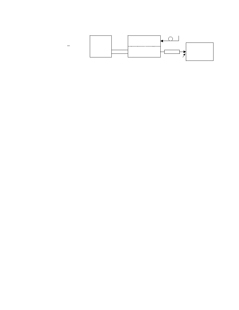
Figure 7. Jitter Generation Test Configuration.
PATTERN
GENERATOR
AGILENT
70841B
Rx
HFCT-5402D
Differential
ECL Data
OmniBER 718A
ATTENUATOR
Input optical
power -14 dBm
Independent SONET
pattern to stimulate Rx.
Tx
Transmitter Disable
The transmitter can be disabled
by connecting pin 7 to the
appropriate voltage (V7 > 4 V). In
normal operation (transmitter
enabled), no external connection
is required.
Transmitter Jitter Generation
The jitter generation requirements
for SONET/SDH transport systems
are:
· 100 m UI pk - pk (SONET)
· 10 m UI rms (SONET/SDH)
Typical jitter generation
performance for the HFCT-5402D
is:
· 60 m UI pk - pk
· 6 m UI rms.
Figure 7 shows the experimental
configuration used to test jitter
generation.
An Agilent 70841B pattern
generator is used to generate ECL
data at 2.48832 Gb/s to modulate
the transmitter. Jitter generation
is measured using a SONET STS48
2
-23
PRBS scrambled pattern.
The optical output of the trans-
mitter is attenuated and fed into
the receiver of the OmniBER 718A
at an input sensitivity of -14 dBm.
Document Outline
- Features
- Applications
- Description
- Transmitter Section
- Receiver Section
- CDR Function
- Reference Clock
- Temperature Range
- Application Information
- Transmitter Section
- Figure 4
- Electrical Characteristics
- Laser Bias Monitor
- Transmitter Disable
- Transmitter Jitter Generation
- Receiver Section
- Reference Clock
- Output Terminations
- Signal Detect
- Jitter Parameters
- Reflectance
- Receiver Operating Wavelength
- Power Supply Filtering
- Figure 16
- Figure 17
- Figure 18
- Evaluation Board
- Application Considerations
- PCB Layout
- EMI Radiation/Susceptibility
- Compatibility Trials
- Recommended Solder and Wash Process
- Process Plug
- Recommended Solder Fluxes and Cleaning/Degreasing Chemicals
- Regulatory Compliance
- Electrostatic Discharge (ESD)
- Electromagnetic Interference (EMI)
- Eye Safety
- Qualification
- Figure 23. Package Outline Drawing and Pinout
- Performance Specifications
- Absolute Maximum Ratings
- Recommended Operating Environment
- Transmitter Section
- Receiver Section
- Table 1. Pin Out Table
- Ordering Information
- Associated Parts