
APT100GF60JU3
A
P
T
1
00G
F
60J
U
3≠ R
e
v 0 A
p
r
i
l
,
2004
APT website ≠ http://www.advancedpower.com
1 - 9
ISOTOP
“
Absolute maximum ratings
Symbol Parameter
Max
ratings
Unit
V
CES
Collector - Emitter Breakdown Voltage
600
V
I
C1
T
C
= 25∞C
120
I
C2
Continuous Collector Current
T
C
= 80∞C
100
I
CM
Pulsed Collector Current
T
C
= 25∞C
320
A
V
GE
Gate ≠ Emitter Voltage
±20
V
P
D
Maximum Power Dissipation
T
C
= 25∞C
416
W
IF
AV
Maximum Average Forward Current
Duty cycle=0.5 T
C
= 80∞C
30
IF
RMS
RMS Forward Current (Square wave, 50% duty)
39
A
These Devices are sensitive to Electrostatic Discharge. Proper Handing Procedures Should Be Followed.
C
A
E
G
V
CES
= 600V
I
C
= 100A @ Tc = 80∞C
Application
∑ AC and DC motor control
∑ Switched Mode Power Supplies
Features
∑ Non Punch Through (NPT) THUNDERBOLT IGBT
Æ
- Low
voltage
drop
- Low tail current
- Switching frequency up to 100 kHz
- Soft recovery parallel diodes
- Low diode VF
- Low leakage current
- Avalanche energy rated
- RBSOA and SCSOA rated
∑ ISOTOP
Æ
Package (SOT-227)
∑ Very low stray inductance
∑ High level of integration
Benefits
∑ Outstanding performance at high frequency operation
∑ Stable temperature behavior
∑ Very rugged
∑ Direct mounting to heatsink (isolated package)
∑ Low junction to case thermal resistance
∑ Easy paralleling due to positive TC of VCEsat
ISOTOP
Æ
Buck chopper
NPT IGBT
A
C
G
E

APT100GF60JU3
A
P
T
1
00G
F
60J
U
3≠ R
e
v 0 A
p
r
i
l
,
2004
APT website ≠ http://www.advancedpower.com
2 - 9
All ratings @ T
j
= 25∞C unless otherwise specified
Electrical Characteristics
Symbol Characteristic
Test
Conditions
Min Typ Max Unit
BV
CES
Collector - Emitter Breakdown Voltage
V
GE
= 0V, I
C
= 100µA
600
V
T
j
= 25∞C
100
I
CES
Zero Gate Voltage Collector Current
V
GE
= 0V
V
CE
= 600V
T
j
= 125∞C
1000
µA
T
j
= 25∞C
2.0
2.5
V
CE(on)
Collector Emitter on Voltage
V
GE
=15V
I
C
= 100A
T
j
= 125∞C
2.2
V
V
GE(th)
Gate Threshold Voltage
V
GE
= V
CE
, I
C
= 1mA
3
5
V
I
GES
Gate ≠ Emitter Leakage Current
V
GE
= ±20V, V
CE
= 0V
±150
nA
Dynamic Characteristics
Symbol Characteristic
Test
Conditions
Min Typ Max Unit
C
ies
Input
Capacitance
4300
C
oes
Output
Capacitance
470
C
res
Reverse Transfer Capacitance
V
GE
= 0V
V
CE
= 25V
f = 1MHz
400
pF
Q
g
Total gate Charge
330
Q
ge
Gate ≠ Emitter Charge
290
Q
gc
Gate ≠ Collector Charge
V
GS
= 15V
V
Bus
= 300V
I
C
= 100A
200
nC
T
d(on)
Turn-on Delay Time
26
T
r
Rise
Time
25
T
d(off)
Turn-off Delay Time
150
T
f
Fall
Time
30
ns
E
on
Turn-on Switching Energy
3.35
E
off
Turn off Switching Energy
Resistive Switching (25∞C)
V
GE
= 15V
V
Bus
= 400V
I
C
= 100A
R
G
= 5
W
2.85
mJ
T
d(on)
Turn-on Delay Time
26
T
r
Rise
Time
25
T
d(off)
Turn-off Delay Time
170
T
f
Fall
Time
40
ns
E
on
Turn-on Switching Energy
4.3
E
off
Turn-off Switching Energy
Inductive Switching (125∞C)
V
GE
= 15V
V
Bus
= 400V
I
C
= 100A
R
G
= 5
W
3.5
mJ

APT100GF60JU3
A
P
T
1
00G
F
60J
U
3≠ R
e
v 0 A
p
r
i
l
,
2004
APT website ≠ http://www.advancedpower.com
3 - 9
Diode ratings and characteristics
Symbol Characteristic
Test
Conditions
Min Typ Max Unit
I
F
= 30A
1.6
1.8
I
F
= 60A
1.9
V
F
Diode Forward Voltage
I
F
= 30A
T
j
= 125∞C
1.4
V
V
R
= 600V
T
j
= 25∞C
250
I
RM
Maximum Reverse Leakage Current
V
R
= 600V
T
j
= 125∞C
500
µA
C
T
Junction
Capacitance
V
R
=
200V
44 pF
Reverse Recovery Time
I
F
=1A,V
R
=30V
di/dt =100A/µs
T
j
= 25∞C
23
T
j
= 25∞C
85
t
rr
Reverse Recovery Time
T
j
= 125∞C
160
ns
T
j
= 25∞C
4
I
RRM
Maximum Reverse Recovery Current
T
j
= 125∞C
8
A
T
j
= 25∞C
130
Q
rr
Reverse Recovery Charge
I
F
= 30A
V
R
= 400V
di/dt =200A/µs
T
j
= 125∞C
700
nC
t
rr
Reverse Recovery Time
70
ns
Q
rr
Reverse Recovery Charge
1300
nC
I
RRM
Maximum Reverse Recovery Current
I
F
= 30A
V
R
= 400V
di/dt =1000A/µs
T
j
= 125∞C
30 A
Thermal and package characteristics
Symbol Characteristic
Min Typ Max Unit
IGBT 0.3
R
thJC
Junction
to
Case
Diode
1.21
R
thJA
Junction to Ambient (IGBT & Diode)
20
∞C/W
V
ISOL
RMS Isolation Voltage, any terminal to case t =1 min, I isol<1mA, 50/60Hz
2500 V
T
J
,T
STG
Storage
Temperature
Range
-55
150
T
L
Max Lead Temp for Soldering:0.063" from case for 10 sec
300
∞C
Torque Mounting
torque
(Mounting = 8-32 or 4mm Machine and terminals = 4mm Machine)
1.5
N.m
Wt Package
Weight
29.2 g

APT100GF60JU3
A
P
T
1
00G
F
60J
U
3≠ R
e
v 0 A
p
r
i
l
,
2004
APT website ≠ http://www.advancedpower.com
4 - 9
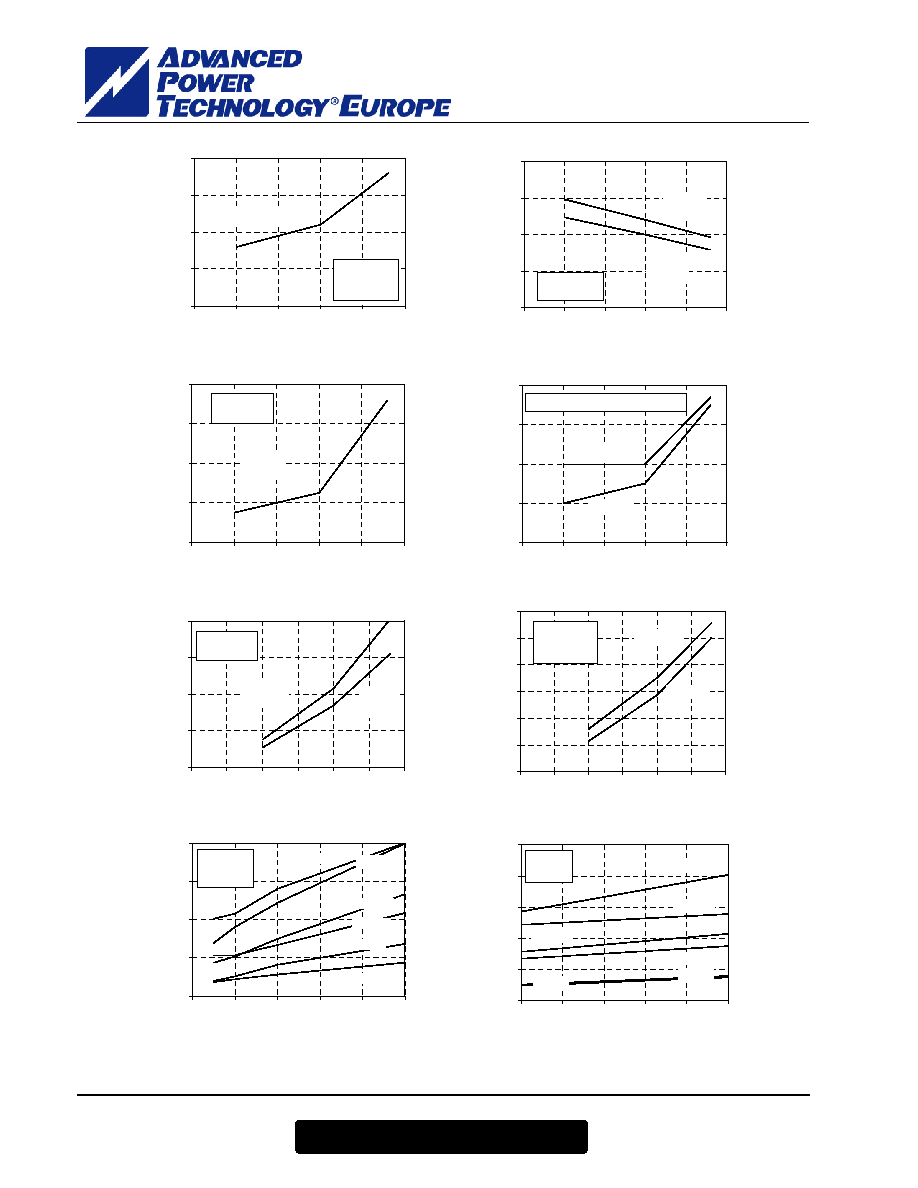
Typical IGBT Performance Curve
Output characteristics (V
GE
=15V)
Tc=-55∞C
Tc=25∞C
Tc=125∞C
0
50
100
150
200
250
300
350
0
1
2
3
4
I
c
, C
o
lle
ct
o
r
C
u
r
r
e
n
t
(
A
)
V
CE
, Collector to Emitter Voltage (V)
250µs Pulse Test
< 0.5% Duty cycle
Output Characteristics (V
GE
=10V)
Tc=-55∞C
Tc=25∞C
Tc=125∞C
0
50
100
150
200
250
300
0
1
2
3
4
Ic,
Co
ll
ect
o
r
Cu
r
r
en
t
(
A
)
V
CE
, Collector to Emitter Voltage (V)
250µs Pulse Test
< 0.5% Duty cycle
Transfer Characteristics
T
J
=-55∞C
T
J
=25∞C
T
J
=125∞C
0
50
100
150
200
250
300
0
1
2
3
4
5
6
7
8
9
10
V
GE
, Gate to Emitter Voltage (V)
Ic,
C
o
lle
ct
o
r
Cu
r
r
en
t
(
A
)
250µs Pulse Test
< 0.5% Duty cycle
Ic=200A
Ic=100A
Ic=50A
0
1
2
3
4
5
6
7
8
6
8
10
12
14
16
V
GE
, Gate to Emitter Voltage (V)
V
CE
, C
o
lle
c
t
or
t
o
E
m
it
t
e
r
V
o
l
t
a
g
e
(
V
) On state Voltage vs Gate to Emitter Volt.
T
J
= 25∞C
250µs Pulse Test
< 0.5% Duty cycle
Ic=200A
Ic=100A
Ic=50A
0
0.5
1
1.5
2
2.5
3
3.5
4
-50
-25
0
25
50
75
100
125
T
J
, Junction Temperature (∞C)
V
CE
, C
o
lle
c
t
or
t
o
E
m
it
t
e
r
V
o
lt
a
g
e
(
V
) On state Voltage vs Junction Temperature
250µs Pulse Test
< 0.5% Duty cycle
V
GE
= 15V
0.70
0.80
0.90
1.00
1.10
1.20
-50
-25
0
25
50
75
100 125
T
J
, Junction Temperature (∞C)
Co
lle
c
t
or t
o
E
m
it
t
e
r
Bre
a
k
dow
n
Vo
l
t
ag
e (N
o
r
ma
l
i
z
e
d
)
Breakdown Voltage vs Junction Temp.
0
20
40
60
80
100
120
140
160
-50 -25
0
25
50
75 100 125 150
T
C
, Case Temperature (∞C)
I
c
,
DC Col
l
e
c
t
o
r
Cu
rre
nt
(
A
)
DC Collector Current vs Case Temperature
Gate Charge
V
CE
=120V
V
CE
=300V
V
CE
=480V
0
2
4
6
8
10
12
14
16
18
0
50
100
150
200
250
300
350
Gate Charge (nC)
V
GE
,
G
a
te to
E
m
i
t
ter
V
o
l
t
a
g
e
(V
)
I
C
= 100A
T
J
= 25∞C
APT100GF60JU3
A
P
T
1
00G
F
60J
U
3≠ R
e
v 0 A
p
r
i
l
,
2004
APT website ≠ http://www.advancedpower.com
5 - 9
V
GE
= 15V
15
20
25
30
35
25
50
75
100
125
150
I
CE
, Collector to Emitter Current (A)
t
d
(
on)
,
Tur
n-
O
n
De
l
a
y
Ti
m
e
(
n
s
)
Turn-On Delay Time vs Collector Current
Tj = 25∞C
V
CE
= 400V
R
G
= 5
V
GE
=15V,
T
J
=25∞C
V
GE
=15V,
T
J
=125∞C
50
100
150
200
250
25
50
75
100
125
150
I
CE
, Collector to Emitter Current (A)
t
d
(
o
f
f
)
,
Tur
n-
O
f
f
De
l
a
y
Ti
m
e
(
n
s
)
Turn-Off Delay Time vs Collector Current
V
CE
= 400V
R
G
= 5
V
GE
=15V,
T
J
=125∞C
0
20
40
60
80
25
50
75
100
125
150
I
CE
, Collector to Emitter Current (A)
t
r
,
R
i
se
T
i
m
e
(
n
s)
Current Rise Time vs Collector Current
V
CE
= 400V
R
G
= 5
T
J
= 25∞C
T
J
= 125∞C
0
20
40
60
80
25
50
75
100
125
150
I
CE
, Collector to Emitter Current (A)
t
f
,
Fa
l
l
Ti
m
e
(
n
s
)
Current Fall Time vs Collector Current
V
CE
= 400V, V
GE
= 15V, R
G
= 5
T
J
=25∞C,
V
GE
=15V
T
J
=125∞C,
V
GE
=15V
0
2
4
6
8
0
25
50
75
100
125
150
I
CE
, Collector to Emitter Current (A)
E
on
,
Tur
n-
O
n
E
n
e
r
gy
Los
s
(
m
J
)
Turn-On Energy Loss vs Collector Current
V
CE
= 400V
R
G
= 5
T
J
= 25∞C
T
J
= 125∞C
0
1
2
3
4
5
6
0
25
50
75
100
125
150
I
CE
, Collector to Emitter Current (A)
E
of
f
,
Tur
n-
of
f
E
n
e
r
gy
Los
s
(
m
J
)
Turn-Off Energy Loss vs Collector Current
V
CE
= 400V
V
GE
= 15V
R
G
= 5
Eon, 200A
Eoff, 200A
Eon, 100A
Eoff, 100A
Eon, 50A
Eoff, 50A
0
4
8
12
16
0
10
20
30
40
50
Gate Resistance (Ohms)
Switching Energy Losses vs Gate Resistance
S
w
i
t
c
h
i
ng E
n
e
r
gy
Los
s
e
s
(
m
J
)
V
CE
= 400V
V
GE
= 15V
T
J
= 125∞C
Eon, 200A
Eoff, 200A
Eon, 100A
Eoff, 100A
Eon, 50A
Eoff, 50A
0
2
4
6
8
10
0
25
50
75
100
125
T
J
, Junction Temperature (∞C)
S
w
i
t
c
h
i
ng E
n
e
r
gy
Los
s
e
s
(
m
J
)
Switching Energy Losses vs Junction Temp.
V
CE
= 400V
V
GE
= 15V
R
G
= 5