- 1 -
ZEN2044F
PROGRAMMABLE UNIVERSAL COUNTER
DESCRIPTION
The
is a 24bit x 4ch. programmable universal counter LSI. The
can count
ZEN2044F
ZEN2044F
phase-shifted pulse signals or up/down pulse signals generated from rotary encoders or linear scales.
Since the counter response speed is as high as 33MHz(MAX), the
can be used in a variety of
ZEN2044F
applications required high speed counting, including digital servo controls and precision measurements. As
ZEN2044F
ZEN2011P.
to command sets, the
has a compatibility with the
The
can also monitor input signals and detect any abnormal input accompanied with noise or
ZEN2044F
other disturbances, so that the reliability of counted values are secured.
1. Features
24bit binary up/down counter x 4ch.
Counter response speed:
33MHz(MAX)(CLK fo=33MHz at 50% duty)
Input frequency of count pulse
Two phase-shifted pulse signal input:
DC-8.25MHz (less than fo x 1/4)
Up/down pulse signal input:
DC-16.5MHz (less than fo x 1/2)
Direction recognition for up/down count
Abnormal input detection circuit
Preload register for the up/down counter
Latch register for the up/down counter
Coincidence detection between reference value and count value
Counter operation mode
Quad/double/single edge evaluation(for two phase-shifted signal / single pulse signal)
Counter direction selection
Count clear control: synchronous/asynchronous
Command mode
Mode 0:
Each channel has one comparator for coincidence detection
Each channel has one port for user input
Mode 1:
Each channel has two comparators for coincidence detection
Each channel has no port for user input
Logical sum output of coincidence detections available
Interrupt output under some conditions available
8bit data bus
Low power CMOS technology
TTL level compatible input
Single 5V power supply
100 pin QFP
Note ) In following chapters;
" " corresponds to a number of the channel(0-3).
n
"*" stands for "Don't care".
Pin Configuration(Top View)
30
31
80
81
100
85
90
95
100
UD/AB2
DIR2
Vdd
Vss
Vdd
SEL30
EXTA3
EXTB3
Z/CLR2
LD3
B/DN3
Vss
SEL0
0
SE
L01
SE
L02
Vss
RESET
Vdd
n.c.
A/UP0 B/DN
0
Z/CLR
0
UD/AB
0
Vss C/D
A
D/CE0
A
D/CE1
A
D/CE2
A
D/CE
3
DRCTC
E
LD0
n.c.
Vss
TEST1
TEST0
Vss
D7
D6
D1
Vdd
A/UP3
D0
Vdd
RD
WR
Vss
n.c.
Vdd
n.c.
1
n.c.
UD/
AB3
D
IR3 Vss
EXTB0 EXTA0
Vdd
SEL32
Vss
D3
D2
D4
5
10
15
20
25
55
60
35
40
45
50
30
65
70
75
80
50
51
B/
DN2
A/
UP2
Vs
s
SEL22 SEL21 SEL20 LT2 LD2 Vss EXTA
2
EX
TB2
Vd
d
Vd
d
CLK Vss DIR1 UD/AB1 Z/CLR1 B/DN
1
A/UP
1
n.c
.
SEL10 LT1 LD1 Vdd EXTA1 EXTB
1
Vss
LT0
TEST
I
D
IR0 n.c.
D5
SE
L11
SE
L12
Vss
LT3
SEL31
Z/CLR3
Z2044G00 ZENIC INC.
(
)

- 2 -
ZEN2044F
2. Block diagram
DRCTCE
Ch.0
AD/CE[3:0]
CPU
C/D
I/F
CE
Status
Mode0,1
EXTA
EXTA0
WR
C/D
rd
reg.
function
EXTB
EXTB0
RD
WR
Command wr
(8bit)
control
RD
decoder
lt
ld
Reference
Comparator
LT0
LT
reg.A(24bit)
A(24bit)
LD0
LD
Reference
Comparator
SEL0[2:0]
SEL[2:0]
reg.B(24bit)
B(24bit)
UD/AB0
UD/AB
Up/down
Latch
DIR0
DIR
Direction
counter
reg.(24bit)
A/UP0
A/UP
recognition
(24bit)
B/DN0
B/DN
for up/down
Z/CLR0
Z/CLR
Preload reg.
(24bit)
D[7:0]
D[7:0]
cnt0
Ch.1
CE
EXTA
EXTA1
C/D
c
EXTB
EXTB1
WR
n
RD
t
LT1
LT
1
LD1
LD
SEL1[2:0]
SEL[2:0]
UD/AB1
UD/AB
DIR1
DIR
A/UP1
A/UP
B/DN1
B/DN
Z/CLR1
Z/CLR
D[7:0]
Ch.2
Ch.3
CE
EXTA
EXTA2
CE
EXTA
EXTA3
C/D
c
EXT
EXTB2
C/D
c
EXTB
EXTB3
B
WR
n
WR
n
RD
t
RD
t
LT2
LT
2
LT3
LT
3
LD2
LD
LD3
LD
SEL2[2:0]
SEL[2:0]
SEL3[2:0]
SEL[2:0]
UD/AB2
UD/AB
UD/AB3
UD/AB
DIR2
DIR
DIR3
DIR
A/UP2
A/UP
A/UP3
A/UP
B/DN2
B/DN
B/DN3
B/DN
Z/CLR2
Z/CLR
Z/CLR3
Z/CLR
CLK
D[7:0]
D[7:0]
RESET
Vdd
Vss
Z2044G00 ZENIC INC.
(
)

- 3 -
Z2044G00 ZENIC INC.
(
)
ZEN2044F
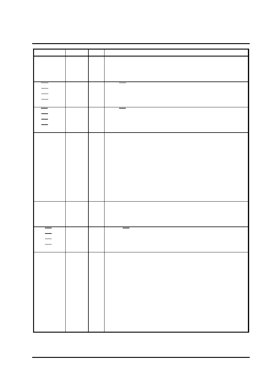
3. Pin description
Table 1
Name
No.
I/O
Function
EXTA0
6
O
The function of this output depends on the command mode. In Mode
EXTA1
53
0, EXTA
outputs the equal signal A(EQA ). In Mode 1, one of the
n
n
EXTA2
71
following three signals can be selected:
EXTA3
86
-The equal signal A(EQA ).
n
-The logical sum(EQA +EQB ) of the equal signal A(EQA ) and
n
n
n
the equal signal B(EQB ).
n
-The hold equal signal A(INTEQA ).
n
CLK
67
I
The CLK synchronizes the internal circuit operation.
RESET
16
I
The RESET initializes the up/down counter, the phase
discrimination circuit, the command register and the status register.
AD/CE0
26
I
The function of these pins depends on the DRCTCE. If DRCTCE="1",
AD/CE1
27
they are all treated as signals for enabling the channel directly. If
AD/CE2
28
DRCTCE="0",AD/CE3 and AD/CE2 are the chip enable pins and
AD/CE3
29
AD/CE1 and AD/CE0 are used to select the channnel.
DRCTCE
30
I
The DRCTCE specifies the mode of the channel select.
C/D
25
I
The C/D defines the type of the data transfered between the CPU
and the ZEN2044F(command or value). This pin is usually connected
with LSB of the address lines.
RD
34
I
The RD is the strobe signal of the read operation.
WR
33
I
The WR is the strobe signal of the write operation.
LD0
8
I
The LD
transmits the 32bit data which is stored in the preload
n
LD1
55
register to the up/down counter.
LD2
73
LD3
88
LT0
9
I
The LT
stores the 32bit data of the up/down counter into the latch
n
LT1
56
register.
LT2
74
LT3
89
D0
36
I/O
These pins are connected with CPU data bus.
D1
37
D2
38
D3
39
D4
42
D5
43
D6
44
D7
45
EXTB0
5
I/O
In Mode 0, EXTB
is used as a general purpose input U of which
n
EXTB1
52
value can be read from the status register. In Mode 1, EXTB
is a
n
EXTB2
70
programable output. One of the following three signals can be
EXTB3
85
selected:
-The equal signal B(EQB )
n
-The signal that indicates detecting an abnormal input(INTAI )
n
-The hold equal signal B(INTEQB )
n
- 4 -
Z2044G00 ZENIC INC.
(
)
ZEN2044F
Name
No.
I/O
Function
Z/CLR0
20
I
The Z/CLR clears the value of the up/down counter. This pin is
n
Z/CLR1
63
usually connected with the index signal of a rotary encoder or a
Z/CLR2
81
linear scale.
Z/CLR3
98
B/DN0
19
I
The B/DN is the count pulse input B or DN.
n
B/DN1
62
B/DN2
80
B/DN3
97
A/UP0
18
I
The A/UP is the count pulse input A or UP.
n
A/UP1
61
A/UP2
79
A/UP3
96
SEL00
10
I
The condition of these three pins(SEL 0, SEL 1 and SEL 2)
n
n
n
SEL01
11
specifies the counter operation mode. See the Table 4.
SEL02
12
SEL10
57
SEL11
58
SEL12
59
SEL20
75
SEL21
76
SEL22
77
SEL30
92
SEL31
93
SEL32
94
DIR0
22
I
The DIR selects the count direction of the up/down counter.
n
DIR1
65
DIR2
83
DIR3
3
UD/AB0
21
I
The UD/AB selects the input pulse mode(up/down or not).
n
UD/AB1
64
UD/AB2
82
UD/AB3
2
Vss
4
-
Ground(0V)
15
24
32
40
46
49
51
66
72
78
87
90
95

- 5 -
Z2044G00 ZENIC INC.
(
)
ZEN2044F
Name
No.
I/O
Function
Vdd
7
-
Supply voltage(+5V)
17
35
41
54
68
69
84
91
99
N.C.
1
-
Not connected.
14
23
31
50
60
100
TEST0
47
I
These test pins MUST be connected with +5V in nomal operation.
TEST1
48
TESTI
13
Note ) Except N.C., the input pins which are not used MUST be connected with Vdd or Ground.
ZEN2044F