VISHAY
SFH6700/ 01/ 02/ 05/ 11/ 12/ 19
Document Number 83683
Rev. 1.3, 27-Apr-04
Vishay Semiconductors
www.vishay.com
1
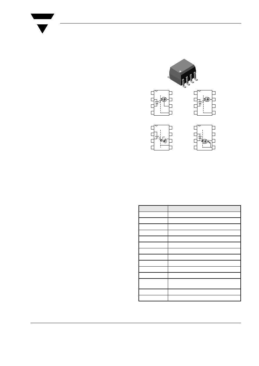
i179073
1
2
3
4
8
7
6
5
VCC
VO
VE
GND
NC
A
C
NC
SFH6700/6719
1
2
3
4
8
7
6
5
VCC
VO
NC
GND
NC
A
C
NC
SFH6701/6711
1
2
3
4
8
7
6
5
VCC
NC
VO
GND
SFH6702/6712
NC
A
C
NC
1
2
3
4
8
7
6
5
VCC
NC
VO
GND
SFH6705
NC
A
C
NC
High Speed Optocoupler, 5 MBd, 1 kV/
µs dV/dt
Features
· Data Rate 5.0 MBits/s
(2.5 MBit/s over Temperature)
· Buffer
· Isolation Test Voltage, 5300 V RMS for 1.0 s
· TTL, LSTTL and CMOS Compatible
· Internal Shield for Very High Common Mode
Transient Immunity
· Wide Supply Voltage Range (4.5 to 15 V)
· Low Input Current (1.6 mA to 5.0 mA)
· Three State Output (SFH6700/ 19)
· Totem Pole Output (SFH6701/ 02/ 11/ 12)
· Open Collector Output (SFH6705)
· Specified from 0 °C to 85 °C
Agency Approvals
· UL - File No. E52744 System Code H or J
· DIN EN 60747-5-2(VDE0884)
DIN EN 60747-5-5 pending
Available with Option 1
Applications
Industrial Control
Replace Pulse Transformers
Routine Logic Interfacing
Motion/Power Control
High Speed Line Receiver
Microprocessor System Interfaces
Computer Peripheral Interfaces
Description
The SFH67xx high speed optocoupler series consists
of a GaAlAs infrared emitting diode, optically coupled
with an integrated photo detector. The detector incor-
porates a Schmitt-Trigger stage for improved noise
immunity. Using the Enable input, the output can
switched to the high ohmic state, which is necessary
for data bus applications. A Faraday shield provides a
common mode transient immunity of 1000 V/
µ at
V
CM
= 50 V for SFH6700/ 01/ 02/ 05 and 2500 V/
µ at
V
CM
= 400 V for SFH6711/ 12/ 19.
The SFH67xx uses an industry standard DIP-8 pack-
age.With standard lead bending, creepage distance
and clearance of
7.0 mm with lead bending options
6, 7, and 9
8 mm are achieved.
Order Information
For additional information on the available options refer to
Option Information.
Part
Remarks
SFH6700
Three State Output, DIP-8
SFH6701
Totem Pole Output, DIP-8
SFH6702
Totem Pole Output, DIP-8
SFH6705
Open Collector Output, DIP-8
SFH6711
Totem Pole Output, DIP-8
SFH6712
Totem Pole Output, DIP-8
SFH6719
Three State Output, DIP-8
SFH6700-X009
Three State Output, SMD-8 (option 9)
SFH6701-X006
Totem Pole Output, DIP-8 400 mil (option 6)
SFH6701-X007
Totem Pole Output, SMD-8 (option 7)
SFH6701-X009
Totem Pole Output, SMD-8 (option 9)
SFH6705-X006
Open Collector Output, DIP-8 400 mil (option
6)
SFH6705-X007
Open Collector Output, SMD-8 (option 7)
SFH6711-X007
Totem Pole Output, SMD-8 (option 7)
www.vishay.com
2
Document Number 83683
Rev. 1.3, 27-Apr-04
VISHAY
SFH6700/ 01/ 02/ 05/ 11/ 12/ 19
Vishay Semiconductors
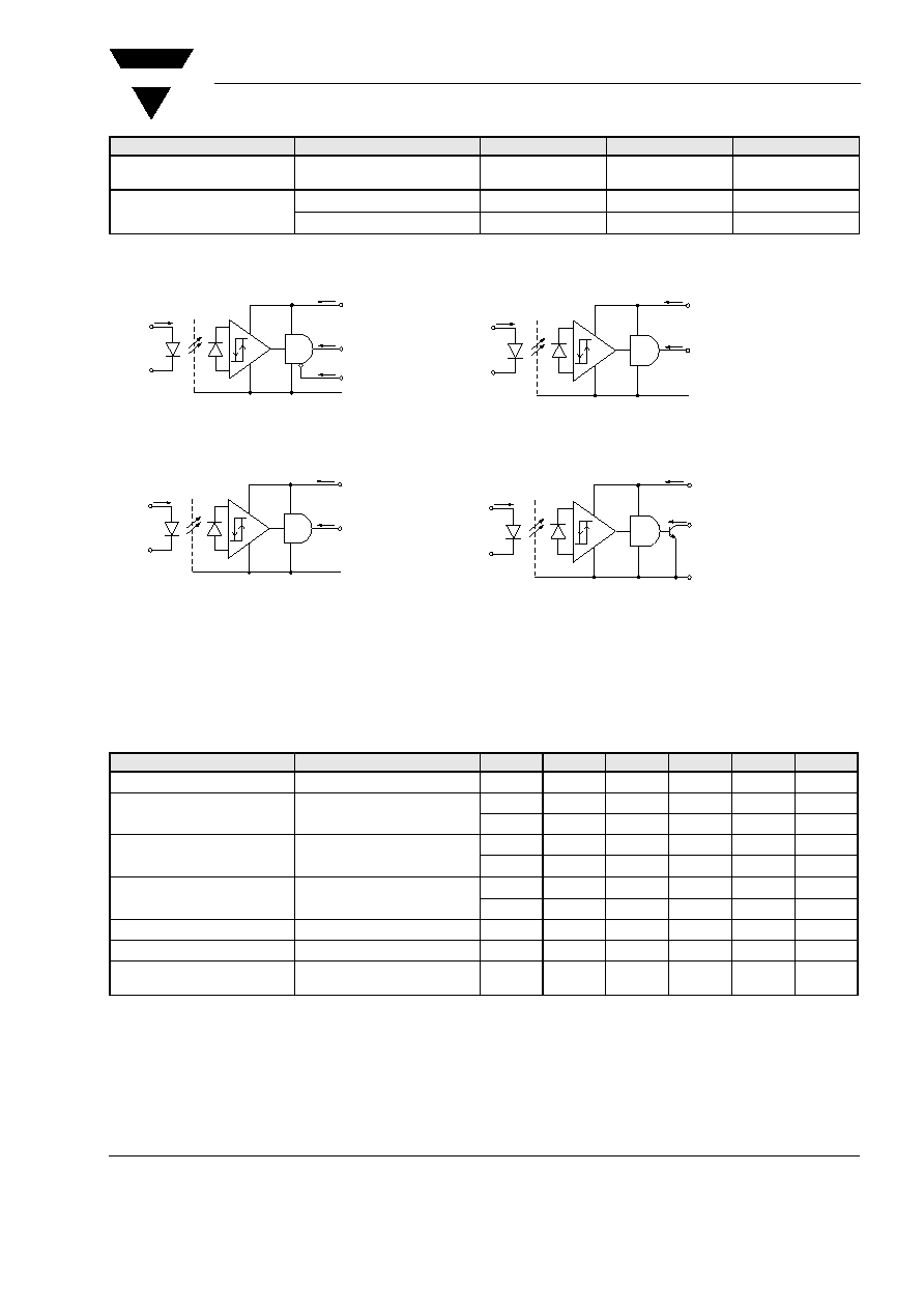
Truth Table (Positive Logic)
Absolute Maximum Ratings
T
amb
= 25 °C, unless otherwise specified
Stresses in excess of the absolute Maximum Ratings can cause permanent damage to the device. Functional operation of the device is
not implied at these or any other conditions in excess of those given in the operational sections of this document. Exposure to absolute
Maximum Rating for extended periods of the time can adversely affect reliability.
Input
Output
Coupler
IR Diode
Enable
Output
SFH6700
on
H
Z
off
H
Z
SFH6719
on
L
H
off
L
L
SFH6701
on
H
off
L
SFH6702
on
H
off
L
SFH6705
on
H
off
L
SFH6711
on
H
off
L
SFH6712
on
H
off
L
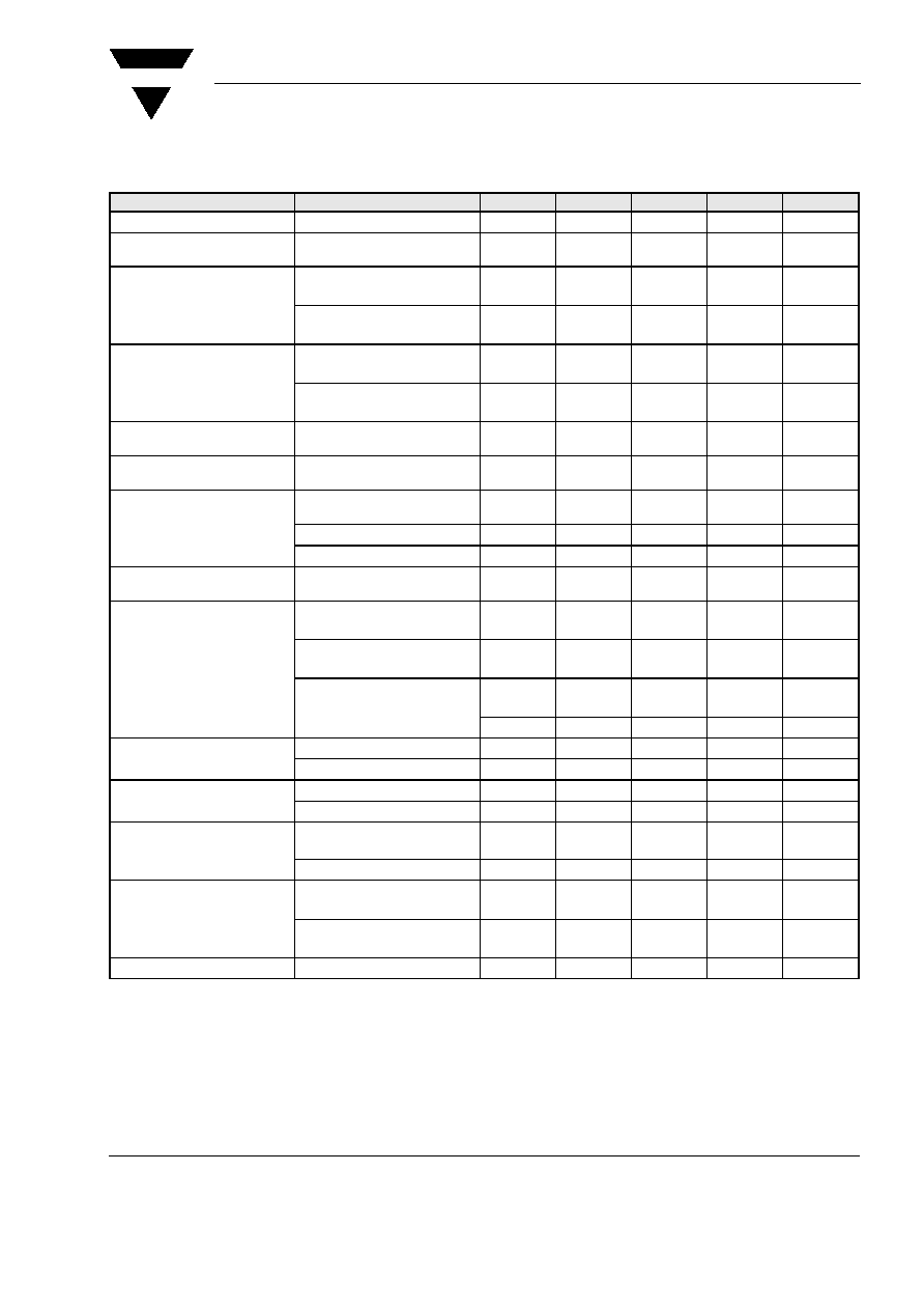
Parameter
Test condition
Symbol
Value
Unit
Reverse voltage
V
R
3.0
V
DC Forward current
I
F
10
mA
Surge forward current
t
1.0 µs
I
FSM
1.0
A
Power dissipation
P
diss
20
mW
Parameter
Test condition
Symbol
Value
Unit
Supply voltage
V
CC
- 0.5 to + 15
V
Three state enable voltage
(SFH6700/19 only)
V
EN
- 0.5 to + 15
V
Output voltage
V
O
- 0.5 to + 15
V
Average output current
I
O
25
mA
Power dissipation
P
diss
100
mW
Parameter
Test condition
Symbol
Value
Unit
Storage temperature range
T
stg
- 55 to + 125
°C
Ambient temperature range
T
amb
- 40 to + 85
°C
Lead soldering temperature
t = 10 s
T
sld
260
°C
Isolation test voltage
V
ISO
5300
V
RMS
Pollution degree
2.0
Creepage distance and
clearance
Standard lead bending
7.0
mm
Options 6, 7, 9
8.0
mm
VISHAY
SFH6700/ 01/ 02/ 05/ 11/ 12/ 19
Document Number 83683
Rev. 1.3, 27-Apr-04
Vishay Semiconductors
www.vishay.com
5
Output
0 °C
T
amb
85 °C; 4.5 V V
CC
15 V; 1.6 mA I
Fon
5.0 mA; 2.0 V
EH
15 V; 0 V
EL
0.8 V; 0 mA I
Foff
0.1 mA;
Typical values: T
amb
= 25 °C; V
CC
= 5.0 V; I
Fon
= 3.0 mA unless otherwise specified
2)
Output short circuit time
10ms.
Parameter
Test condition
Symbol
Min
Typ.
Max
Unit
Logic low output voltage
I
OL
= 6.4 mA
V
OL
0.5
V
Logic high output voltage
(except SFH6705)
I
OH
= 2.6 mA, V
OH
= V
CC
-1.8 V
2.4
V
Output leakage current
(V
OUT
>V
CC
) (except SFH6705)
V
O
= 5.5 V, V
CC
= 4.5 V,
I
F
= 5.0 mA
I
OHH
0.5
100
µA
V
O
= 15 V, V
CC
= 4.5 V,
I
F
= 5.0 mA
I
OHH
1.0
500
µA
Output leakage current
(SFH705 only)
V
O
= 5.5 V, V
CC
= 5.5 V,
I
F
= 5.0 mA
I
OHH
0.5
100
µA
V
O
= 15 V, V
CC
= 15 V,
I
F
= 5.0 mA
I
OHH
1.0
500
µA
Logic high enable voltage
(SFH6700/19 only)
V
EH
2.0
V
Logic low enable voltage
(SFH6700/19 only)
V
EL
0.8
V
Logic high enable current
(SFH6700/19 only)
V
EN
= 2.7 V
I
EH
20
µA
V
EN
= 5.5 V
I
EH
100
µA
V
EN
= 15 V
I
EH
0.001
250
µA
Logic low enable current
(SFH6700/19 only)
V
EN
= 0.4 V
I
EL
- 320
- 50
µA
High impedance state output
current (SFH6700/19 only)
V
O
= 0.4 V, V
EN
= 2.0 V,
I
F
= 5.0 mA
I
OZL
- 20
µA
V
O
= 2.4 V, V
EN
= 2.0 V,
I
F
= 0 mA
I
OZH
20
µA
V
O
= 5.5 V, V
EN
= 2.0 V,
I
F
= 0 mA
I
OZH
100
µA
I
OZH
0.001
500
µA
Logic low supply current
V
CC
= 5.5 V, I
F
= 0
I
CCL
3.7
6.0
mA
V
CC
= 15 V, I
F
= 0
I
CCL
4.1
6.5
mA
Logic high supply current
V
CC
= 5.5 V, I
F
= 5.0 mA
I
CCH
3.4
4.0
mA
V
CC
= 15V, I
F
= 5.0 mA
I
CCH
3.7
5.0
mA
Logic low short circuit output
current
2)
V
O
= V
CC
= 5.5 V, I
F
= 0
I
OSL
25
mA
V
O
= V
CC
= 15 V, I
F
= 0
I
OSL
40
mA
Logic high short circuit output
current
2)
V
CC
= 5.5 V, V
O
= 0 V,
I
F
= 5.0 mA
I
OSL
- 10
mA
V
CC
= 15 V, V
O
= 0 V,
I
F
= 5.0 mA
I
OSL
- 25
mA
Thermal resistance
R
thja
300
K/W