 | –≠–ª–µ–∫—Ç—Ä–æ–Ω–Ω—ã–π –∫–æ–º–ø–æ–Ω–µ–Ω—Ç: TQ7M35 | –°–∫–∞—á–∞—Ç—å:  PDF PDF  ZIP ZIP |

WIRELESS COMMUNICATIONS DIVISION
For additional information and latest specifications, see our website: www.triquint.com
1
Preliminary: Subject to
change without notice
˜4
VGA
Control
CELL_LO
PCS_LO
VCC
TCXO
VCC
LPF
VCO_TANK1
VCO_TANK2
V
CC_
B
U
S
CL
DA
EN
I+
I-
Q+
Q-
IREF
IF_OUT (-)
IF_OUT (+)
UP_IN (-)
UP_IN (+)
VCC
VCNTRL
P
W
R_
UP
C
E
LL_
B
C
E
LL_
A
VC
C
PC
S
_
B
PC
S
_
A
A
B
_
SEL
VC
C
VCC
VCO
VGA
Phase
Shifter
DA
DA
DA
DA
Divider
PFD
CP
˜2
Phase
Shifter
Phase
Shifter
VGA
Product Description:
The TQ7M35 is a 2.7VDC SiGe HBT transmitter designed for use in CDMA mobile
phones. Its RF performance meets the requirements for products designed to IS-95/98
standards. It incorporates the complete transmitter chain for dual-band triple-mode
CDMA phones. The device integrates an I/Q modulator, variable gain amplifier (VGA),
two single side-band up-conversion mixers with fully integrated LO phase shifters, and
a voltage controlled oscillator. It also includes a complete PLL with dividers, phase-
frequency detector (PFD), and a charge pump.
The TQ7M35 provides programmable output power in cellular and PCS bands. The IC
is available in a small 5x5mm, lead-less 32pin quad flat package.
Electrical Specifications:
Parameter
Min
Typ
Max
Units
Frequency Ranges-Cell Band
Frequency Ranges-PCS Band
824
1750
849
1910
MHz
MHz
CDMA mode/Cell Band Pout
1
8
dBm
CDMA Mode/Cell Band ACPR
1
54
dBc
CDMA Mode/PCS Band Pout
2
8
dBm
CDMA Mode/PCS Band ACPR
2
54
dBc
Current consumption
103
mA
Note 1:
Test Conditions CDMA Mode/Cell Band: V
CC
= 3.00VDC, Tc=25∞C
Note 2:
Test Conditions CDMA Mode/PCS Band: V
CC
= 3.00VDC, Tc=25∞C
TQ7M35
DATA SHEET
3V HBT SiGe CDMA
Transmitter
Features
ß
Low 2.7VDC Operation
ß
Single Side-band Up-converters
ß
100dB of Dynamic Range
ß
Low Current Consumption
ß
Individual Block Power Down Capability
ß
On-chip PLL
ß
3-wire bus, 4 bit programming
ß
Full ESD Protection
Applications
ß
Dual Mode and Tri Mode CDMA/AMPS
phones

TQ7M35 - Preliminary
Data Sheet
For additional information and latest specifications, see our website: www.triquint.com
2
Package Pinout:
˜4
VGA
Control
CELL_LO
PCS_LO
VCC_LO
TCXO
VCC
LPF
VCO_TANK1
VCO_TANK2
VC
C_
B
U
S
CL
DA
EN
I+
I-
Q+
Q-
IREF
IF_OUT (-)
IF_OUT (+)
UP_IN (-)
UP_IN (+)
VCC
VCNTRL
PW
R_
U
P
CE
L
L
_
B
CE
L
L
_
A
VC
C
PC
S_
B
PC
S_
A
AB
_
S
E
L
VC
C
VCC
VCO
VGA
Phase
Shifter
DA
DA
DA
DA
Divider
PFD
CP
˜2
1
2
3
4
5
6
7
8
19
15
16
17
18
14
9
10
11
12
13
24
23
22
21
20
28
26
25
27
29
30
31
32
Phase
Shifter
Phase
Shifter
VGA
Preliminary - TQ7M35
For additional information and latest specifications, see our website: www.triquint.com
3
Pin Descriptions:
Pin Name
Pin #
Description and Usage (Equivalent Circuit)
CELL_LO
1
Local oscillator CELL band input
PCS_LO
2
Local oscillator PCS band input
V
CC
3
Regulated power supply
TCXO
4
Reference oscillator input
V
CC
5
Regulated power supply
LPF
6
Charge-pump loop filter
VCO_TANK1
7
Voltage controlled oscillator external tank circuit
VCO_TANK2
8
Voltage controlled oscillator external tank circuit
V
CC_BUS
9
Serial bus interface regulated power supply
CL
10
Serial bus interface clock input
DA
11
Serial bus interface data input
EN
12
Serial bus interface enable strobe input
I+
13
I+ data differential signal input
I-
14
I- data differential signal input
Q+
15
Q+ data differential signal input
Q-
16
Q- data differential signal input
Iref
17
Constant current sink
IF_OUT(-)
18
IF section differential output
IF_OUT(+)
19
IF section differential output
UP_IN(+)
20
Up-converter input
UP_IN(-1)
21
Up-converter input
V
CC
22
Regulated power supply
V
CC
23
Regulated power supply
V
CNTRL
24
Gain control analog voltage input
PWR_UP
25
Power-up logic control signal input. Logic high will power up the integrated circuit except the phase lock loop circuitry
and logic low will power down the integrated circuit except the phase lock loop circuitry.
CELL_B
26
CELL band driver amplifier B open collector power output
CELL_A
27
CELL band driver amplifier A open collector power output
V
CC
28
Regulated power supply
PCS_B
29
PCS band driver amplifier B open collector power output
PCS_A
30
PCS band driver amplifier A open collector power output
AB_Sel
31
Channel select logic control. Logic low will turn-on the A driver output and logic high will enable the B driver output.
V
CC
32
Regulated power supply
GND
Paddle
Ground. TriQuint recommends use of several via holes to the backside ground under the Paddle.

TQ7M35 - Preliminary
Data Sheet
For additional information and latest specifications, see our website: www.triquint.com
4
Output Electrical Characterisitics
1,2
Parameter
Conditions
Min.
Typ/Nom
Max.
Units
Cell Band RF Output (CELL_A, pin
#27 and CELL_B, pin #26)
Cell Band RF Output Frequency
Range
824
849
MHz
Cell Band RF Output Power
High Power (Pout=7.7dBm)
7.7
dBm
Cell Band RF Output Adjacent
Channel Power
High Power Power (Pout=7.7dBm)
-54
dBc
Cell Band RF Output Receive
Band Noise
High Power Power (Pout=7.7dBm)
-130
dBm/Hz
PCS Band RF Output (PCS_A, pin
#30 and PCS_B, pin #29)
PCS Band RF Output Frequency
Range
1750
1910
MHz
PCS Band RF Output Power
High Power (Pout=8.2dBm)
8.2
dBm
PCS Band RF Output Adjacent
Channel Power
High Power (Pout=8.2dBm)
-54
dBc
PCS Band RF Output Receive
Band Noise
High Power (Pout=8.2dBm)
-132
dBm/Hz
IF Section Outputs
(IF_OUT(+), pin #19 and
IF_OUT(-), pin #18)
IF Section Frequency Range
130.38
MHz
IF Section Output Power
-13
dBm
IF Section Adjacent Channel
Power
400 Ohm differential load
-63
dBc
IF Section Carrier Suppression
I/Q input: Differential Sin and Cos signals with
200 mV amplitude (400 mVpp) and 100kHz
frequency from a low ohmic source (<1kOhm)
-35
dBc
IF Section Sideband
Suppression
I/Q input: Differential Sin and Cos signals with
200 mV amplitude (400 mVpp) and 100kHz
frequency from a low ohmic source (<1kOhm)
-50
dBc
Preliminary - TQ7M35
For additional information and latest specifications, see our website: www.triquint.com
5
Output Electrical Characteristics
1,2
(cont'd)
IF Section spurious
I/Q input: Differential Sin and Cos signals with
200 mV amplitude (400 mVpp) and 100kHz
frequency from low ohmic source (<1kOhm)
-60
dBc
IF Section Modulator Noise
@5MHz off carrier
142
dBm/Hz
Note 1: Test Conditions: V
CC
=3.00VDC, TriQuint Test Board, Tc=25
∞
C unless otherwise specified.
Note 2: Min./Max. limits are at +25
∞
C case temperature unless otherwise specified.
Up-converter Electrical Characterisitics
1,2
Parameter
Conditions
Min.
Typ/Nom
Max.
Units
Cellular Band Up-Converter
Cellular Up-Converter output
frequency
824
849
MHz
Cellular Up-Converter IF input power
at UP_IN(+) and UP_IN(-)
f
IF
=130.38MHz
-16
dBm
Cellular Up-Converter Mixer LO Input
Power at Cell_LO
f
LO
=954MHz to 979MHz
-10
-3
dBm
Cellular Up-converter LO-Leakage at
Cell_A or Cell_B
P
LO
=-3dBm
-25
-20
dBm
Cellular Up-converter Image
Rejection at Cell_A or Cell_B
P
RF_OUT
=+7.7dBm
-35
-30
dBc
PCS Band Up-Converter
PCS Up-Converter output frequency
1750
1910
MHz
PCS Up-Converter IF input power at
UP_IN(+) and UP_IN(-)
f
IF
=130.38MHz
-16
dBm
PCS Up-Converter Mixer LO Input
Power at PCS_LO
f
LO
=1620MHz to 1780MHz
-10
-3
dBm
PCS Up-converter LO-Leakage at
PCS_A or PCS_B
P
LO
= -3dBm
-25
-20
dBm
PCS Up-converter Image Rejection
at PCS_A or PCS_B
P
RF_OUT
=+8.2Bm
-35
-30
dBc
Note 1: Test Conditions: V
CC
=3.00VDC, TriQuint Test Board, Tc=25
∞
C unless otherwise specified.
Note 2: Min./Max. limits are at +25
∞
C case temperature unless otherwise specified.

TQ7M35 - Preliminary
Data Sheet
For additional information and latest specifications, see our website: www.triquint.com
6
Absolute Maximum Ratings
Parameter
Absolute Maximum
Value
Units
Supply Voltages (All Vcc pins)
4.0
VDC
Current at any input/output pin
40
mA
Case Temperature, Survival
-30 to +85
∞C
Storage Temperature
-40 to +150
∞C
Note: The part may not survive all maximums applied simultaneously.
Operating Range
Parameter
Range
Units
Supply Voltages (All Vcc pins)
2.7 to 3.3
VDC
Case Temperature
-30 to 85
∞C
DC Supply Electrical Characterisitics
1,2,3
Parameter
Conditions
Min.
Typ/Nom
Max.
Units
Supply Voltages (All Vcc pins)
2.7
3.3
VDC
Cell Band Mode Current Consumption
(Driver A or Driver B activated)
High Power (Pwr_up=1, Bit1=0, Bit2=0, AB_SEL=high
or low, Pout=7.7dBm)
Low Power (Pwr_up=1, Bit1=0, Bit2=0, AB_SEL=high
or low, Pout=-90dBm)
103
90
mA
mA
PCS Band Mode Current Consumption
(Driver A or Driver B activated)
High Power (Pwr_up=1, Bit1=1, Bit2=0, AB_SEL=high
or low, Pout=8.2dBm)
Low Power (Pwr_up=1, Bit1=1, Bit2=1, AB_SEL=high
or low, Pout=-90)
103
90
mA
mA

Preliminary - TQ7M35
For additional information and latest specifications, see our website: www.triquint.com
7
DC Supply Electrical Characterisitics
1,2,3
(Cont'd)
Cell Band Mode Current Consumption
(Driver A and Driver B activated)
High Power (Pwr_up=1, Bit1=0, Bit2=1, Pout=10.7dBm)
Low Power (Pwr_up=1, Bit1=0, Bit2=1, Pout=-87dBm)
120
90
mA
mA
PCS Band Mode Current Consumption
(Driver A and Driver B activated)
High Power (Pwr_up = 1, Bit1=1, Bit2=1, Pout=11dBm)
Low Power (Pwr_up=1, Bit1=1, Bit2=1, Pout=-87dBm)
120
90
mA
mA
Standby Mode Current Consumption
(PLL circuitry, partial IQ modulator
circuitry, and Serial Bus Interface
activated)
Pwr_Up=low, Bit3=1
12
mA
Serial Bus Current Consumption
(Serial Bus Interface activated)
Vcc_bus=High (powered on)
0.7
mA
Powered Off
Pwr_up=low, bit3=0, Vcc_bus=low (powered off)
<10
µ
A
Note 1: Test Conditions: V
CC
=3.00VDC, Tc=25
∞
C unless otherwise specified.
Note 2: Min./Max. limits are at +25
∞
C case temperature unless otherwise specified.
Note 3: TriQuint Test Board.
Analog/RF/IF Input Electrical Characterisitics
1,2,3
Parameter
Conditions
Min.
Typ/Nom
Max.
Units
TCXO Input (TCXO, pin #4)
TCXO Frequency Range
19.68
MHz
TCXO Input Voltage Range
100
250
600
mVp
Cell LO Input (CELL_LO, pin #1)
Cell LO Frequency range
954
979
MHz
Cell LO Input Power Range
50
Source
-10
-3
dBm
Cell LO Input Impedance
(Re{Z
CELL_LO
})
Cell LO Input Frequency (f
LOC
) = 966MHz,
Pwr_Up=0 or 1
43
PCS LO Input (PCS_LO, pin #2)
PCS LO Frequency range (f
LOP
)
1620
1780
MHz
PCS LO Input Power Range (P
LOP
)
50
Source
-10
-3
dBm
PCS LO Input Impedance
(Re{Z
PCS_LO
})
PCS LO Input Frequency (f
LOP
) = 1750MHz,
Pwr_Up=0 or 1
43

TQ7M35 - Preliminary
Data Sheet
For additional information and latest specifications, see our website: www.triquint.com
8
Analog/RF/IF Input Electrical Characteristics
1,2,3
(cont'd)
Up-Converter Input
(UP_IN(+)--pin #21, UP_IN(-)--pin #20)
Up-converter frequency range (f
VGA
)
400 Ohm Source
130.38
MHz
Up-converter power
400 Ohm Source
-16
dBm
Up-converter input impedance
2000
Ohm
Control Voltage Input
(V
CNTRL
, pin #24)
Control voltage input voltage range
0
2.5
VDC
Control voltage input impedance
5000
Ohm
I/Q Modulator base-band inputs
(I+, I-, Q+, Q-, pins #13, 14, 15, and 16)
DC Voltage
Referred to GND
1.35
Vcc/2
Vcc/2 + 0.1
VDC
Frequency Range
0
2MHz
MHz
AC Voltage
Referred to GND
130
mVpp
AC Voltage
Differential
260
mVpp
I/Q Modulator Local Oscillator Input
(VCO_Tank1, pin#7 and VCO_Tank2,
pin #8))
Resonator Frequency Range
520
MHz
Resonator Q
Unloaded
40
None
Note 1: Test Conditions: V
CC
=3.00VDC, Tc=25
∞
C unless otherwise specified.
Note 2: Min./Max. limits are at +25
∞
C case temperature unless otherwise specified.
Note 3: TriQuint Test Board

Preliminary - TQ7M35
For additional information and latest specifications, see our website: www.triquint.com
9
Logical
Input Electrical Characterisitics
1,2,3
Parameter
Conditions
Min.
Typ/Nom
Max.
Units
Logic Input Electrical Characteristics
Applicable to PWR_UP (pin #25), and AB_SEL
(pin #31)
Logical High Voltage Level
Vcc ≠ 0.3
3
Vcc
VDC
Logical Low Voltage Level
0
0
0.3
VDC
Logical Low or High Current
Consumption
50
µ
A
Note 1: Test Conditions: V
CC
=3.00VDC, Tc=25
∞
C unless otherwise specified.
Note 2: Min./Max. limits are at +25
∞
C case temperature unless otherwise specified.
Note 3: TriQuint Test Board
Logical Input Function Selection Table
1
Logical Input
Logical Low
Description
PWR_UP
High
Transmit integrated circuit powered up
PWR_UP
Low
Transmit integrated circuit powered off (PLL with Bit 3 active)
DRV_SEL
High
Driver B active if Bit 2 is low, no effect if Bit 2 is high
DRV_SEL
Low
Driver A active if Bit 2 is low, no effect if Bit 2 is high
Note 1:
A complete truth table is shown below in "Mode Programming Truth Table"
3-Wire Bus
Signal Times
1,2,3
Parameter
Conditions
Min.
Typ/Nom
Max.
Units
3-Wire Bus
Applicable to CL (pin #10), DA (pin #25), and
EN (pin #31)
Clock Period (TPER)
100
ns
Rise Time (TR)
10
ns
Fall Time (TF)
10
ns
Set time data to clock (TS)
35
ns
Hold time data to clock (TH)
35
ns
Clock pulse width (TC)
50
ns
Set time enable to clock (TL)
40
ns
Set time data to neg. going clock
edge (TSC)
10
ns
Note 1:
Test Conditions: V
CC
=3.00VDC, Tc=25
∞
C unless otherwise specified.
Note 2:
Min./Max. limits are at +25
∞
C case temperature unless otherwise specified.
Note 3:
TriQuint Test Board

TQ7M35 - Preliminary
Data Sheet
For additional information and latest specifications, see our website: www.triquint.com
10
3-Wire Bus
Input Timing Diagram
TL
TPER
TC
TS
DA
CK
EN
Mode Programming Truth Table
1
3-Wire Bus Bit Inputs
Logical Inputs
Mode
Bit 4
Bit 3
Bit 2
Bit 1
PWR_UP
AB_SEL
PLL Off
PLL circuitry and partial IQ
modulator circuitry deactivated
X
0
X
X
X
X
PLL On
PLL circuitry and partial IQ
modulator circuitry activated
X
1
X
X
X
X
Transmitter On
Complete IQ modulator circuitry, RF
up-converters, and IF VGA activated
X
X
X
X
High
X
Transmitter Off
Complete IQ modulator circuitry, RF
up-converters, and IF VGA
deactivated
X
X
X
X
Low
X
Driver A (Cell Band DA A activated)
X
X
0
0
High
Low
Driver B (Cell Band DA B activated)
X
X
0
0
High
High
Cell Mode
Driver A and B (Cell Band DA A and
B activated)
X
X
1
0
High
X
Driver A (PCS Band DA A activated)
X
X
0
1
High
Low
Driver B (Cell Band DA B activated)
X
X
0
1
High
High
PCS Mode
Driver A and B (Cell Band DA A and
B activated)
X
X
1
1
High
X
1
The symbol X ("don't care") means a logic input does not affect an operating mode.

Preliminary - TQ7M35
For additional information and latest specifications, see our website: www.triquint.com
11
Measured Performance, CDMA Modulation:
Test Conditions (Unless Otherwise Specified): V
CC
=3.0VDC, Tc=+25∞C, Cell Band freq=836MHz, PCS Band freq=1880MHz
ACPR vs. Vcc vs. Pout - CDMA MODE
Cell Band Driver B
-75
-70
-65
-60
-55
-50
0
5
10
Power (dBm)
ACPR (dBc)
2.7 V
3.0 V
3.3 V
Pout vs. Vcc vs. Vcntrl - CDMA Mode
Cell Band Driver B
-60
-50
-40
-30
-20
-10
0
10
0.9 1.0 1.1 1.2 1.3 1.4 1.5 1.6 1.7 1.8 1.9 2.0 2.1 2.2 2.3
VCNTRL (V)
Pow
e
r (dBm
)
2.7V, 3.0V, 3.3V
Pout vs. Ta vs. Vcntrl - CDMA Mode
Cell Band Driver B
-60
-50
-40
-30
-20
-10
0
10
0.9 1.0 1.1 1.2 1.3 1.4 1.5 1.6 1.7 1.8 1.9 2.0 2.1 2.2 2.3
VCNTRL (V)
Pout (dBm)
-40∞C, 25∞C, 85∞C
ACPR vs. Vcc vs. Pout - CDMA Mode
PCS Band Driver B
-75
-70
-65
-60
-55
-50
0
5
10
Power (dBm)
AC
PR
(
d
Bc
)
2.7 V
3.0 V
3.3 V
Pout vs. Vcc vs. Vcntrl - CDMA Mode
PCS Band Driver B
-60
-50
-40
-30
-20
-10
0
10
0.9 1.0 1.1 1.2 1.3 1.4 1.5 1.6 1.7 1.8 1.9 2.0 2.1 2.2 2.3 2.4 2.5
VCNTRL (V)
Pow
e
r (dB
m
)
2.7V, 3.0V, 3.3V
Pout vs. Ta vs. Vcntrl - CDMA Mode
PCS Band Driver B
-60
-50
-40
-30
-20
-10
0
10
20
0.9 1.0 1.1 1.2 1.3 1.4 1.5 1.6 1.7 1.8 1.9 2.0 2.1 2.2 2.3 2.4 2.5
VCNTRL (V)
Pout (dBm)
-40∞C, 25∞C, 85∞C

TQ7M35-Preliminary
Data Sheet
12
For additional information and latest specifications, see our website: www.triquint.com
Application/Test Circuit:
Cell LO In
PCS LO In
Vcc_LO
TCXO In
CELL_LO
PCS_LO
VCC_LO
TCXO
VCC_CP
LPF
VCO_TANK1
VCO_TANK2
VC
C
_
B
U
S
CL
DA
EN
I+
I
-
Q+
Q
-
IREF
TANK4
TANK3
TANK2
TANK1
VCC_VGA
VCNTRL
P
W
R_UP
C
E
LL_B
C
E
LL_A
V
C
C_
DRV
PCS_
B
PCS_
A
AB_
SE
L
VCC_
I
Q
VCC_MI
X
1
2
3
4
5
6
7
8
19
15
16
17
18
14
9
10
11
12
13
24
23
22
21
20
28
26
25
27
29
30
31
32
R3
C26
C21
R2
R5
R10
D1
C20
C22
L5
C23
C24
C28
R4
C27
C2
C3
Vcc_CP
Vcc_BUS Clock Data Enable I+
I-
Q+
Q-
Iref
C19
8-OUT2
7-nc
6-nc
5-OUT1
IN1-1
nc-2
nc-3
IN2-4
GND
9
C16
C14
C13
Vcc_MIX
Vcc_VGA
Vcntrl
C39
C38
C34
C33
Pwr_Up
Reg. Vcc
Reg. Vcc
Vcc_DRV
C33
C32
AB_Sel
Reg. Vcc
TQ7M35
C29
C25
C30
C31
R17
R18
R19
R20
F1
PCS_A
PCS_B
CELL_A
CELL_B
C4
C5
C6
C7
C37
C36
C11
C10
L4
L2
L3
L1
J2
J7
J3
J4
J5
J6
J25
C18
C17
Bill of Material for TQ7M35 CDMA Transmitter*
Component
Reference
Designator
Part
Number
Value
Size
CDMA Transmitter
TQ7M35
32pin/5mm square
RF Connectors
J2, J3, J4, J5, J6,
J7, J25
Capacitor
C23
1.2pF
0402
Capacitor
C21
6.8pF
0402
Capacitor
C20, C22, C27
8.2pF
0402
Capacitor
C4, C5
22pF
0402
Capacitor
C30, C31
68pF
0402

Preliminary - TQ7M35
Data Sheet
For additional information and latest specifications, see our website: www.triquint.com
13
Bill of Material for TQ7M35 CDMA Transmitter* (cont'd)
Component
Reference
Designator
Part
Number
Value
Size
Capacitor
C2, C6, C7, C8,
C11, C18, C24,
C29, C32, C34,
C37, C39
100pF
0402
Capacitor
C26
120pF
0402
Capacitor
C13, C14, C16, C19
10nF
0402
Capacitor
C3, C9, C10, C17,
C25, C28, C33,
C35, C36, C38
100nF
0402
Resistor
R5, R17, R18, R19,
R20
1K Ohm
0402
Resistor
R2, R10
2.7K Ohm
0402
Resistor
R4
3.3K Ohm
0402
Resistor
R3
27K Ohm
0402
Inductor
L1, L3
4.7nH
0402
Inductor
L2, L4
15nH
0402
Inductor
L5
0603CS-18NX
Coilcraft
18nH
0603
Varactor-Diode
D1
Alpha
SMV1235-074
Filter
F1
LFSH30N/nc
(Murata)
130.38MHz
LFSH30
*May vary due to printed circuit board layout and material
TQ7M35-Preliminary
Data Sheet
14
For additional information and latest specifications, see our website: www.triquint.com
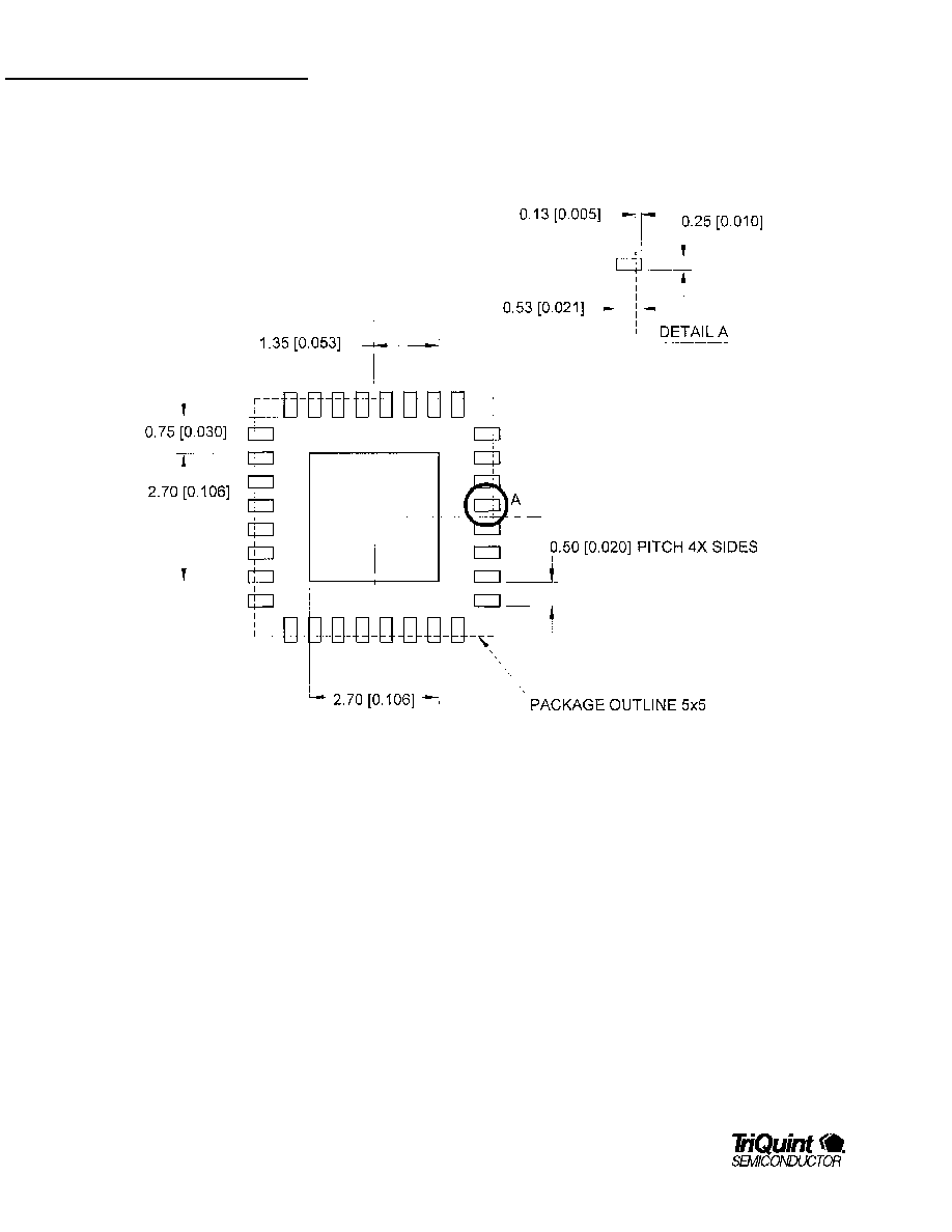
Recommended PC board layout to Accept 32 Pin Plastic Package:
Notes:
1 Only ground signal traces are allowed directly under the package
2 Primary dimensions are in millimeters alternate dimensions in brackets are in inches.

Preliminary -TQ7M35
Data Sheet
For additional information and latest specifications, see our website: www.triquint.com
15
Package Type: 32 Pin Lead-less Plastic Package
CC
DD
BB
AA
Detail X
Detail X
Pin 1
E
D
A
D2
E2
e
b
L
LASER MARK
PIN 1 ID
JEDEC DESIGNATION DESCRIPTION
METRIC
ENGLISH
NOTE
A
OVERALL HEIGHT
0.90 +/-.10 mm
.035 +/-.004 in
1
b
TERMINAL WIDTH
0.23 +/-.07 mm
.009 +/-.003 in
1
D
PACKAGE LENGTH
5.00 mm BSC
.197 in
1
D2
EXOPSED PAD LENGTH
3.45 +/-.10 mm
.136 +/-.004 in
1
e
TERMINAL PITCH
0.50 mm BSC
.020 in
1
E
PACKAGE WIDTH
5.00 mm BSC
.197 in
1
E2
EXPOSED PAD WIDTH
3.45 +/-.10 mm
.136 +/-.004 in
1
L
TERMINAL LENGTH
0.40 +/-.10 mm
.016 +/-.004 in
1
AA
PIN 1 ID LENGTH
0.23 mm BSC
.009 in
1
BB
PIN 1 ID WIDTH
0.23 mm BSC
.009 in
1
CC
PIN 1 ID TO EDGE
0.18 mm BSC
.007 in
1
DD
PIN 1 ID TO EDGE
0.18 mm BSC
.007 in
1
Notes:
Primary dimensions are in metric millimeters. The English equivalents are calculated and subject to rounding error.
Additional Information
For latest specifications, additional product information, worldwide sales and distribution locations, and information about TriQuint:
Web: www.triquint.com
Tel: (503) 615-9000
Email: info_wireless@tqs.com
Fax: (503) 615-8902
For technical questions and additional information on specific applications:
Email: info_wireless@tqs.com
The information provided herein is believed to be reliable; TriQuint assumes no liability for inaccuracies or omissions. TriQuint assumes no responsibility for the use of
this information, and all such information shall be entirely at the user's own risk. Prices and specifications are subject to change without notice. No patent rights or
licenses to any of the circuits described herein are implied or granted to any third party.
TriQuint does not authorize or warrant any TriQuint product for use in life-support devices and/or systems.
Copyright © 2001 TriQuint Semiconductor, Inc. All rights reserved.
Revision 0.15 December 14, 2001