 | –≠–Ľ–Ķ–ļ—ā—Ä–ĺ–Ĺ–Ĺ—č–Ļ –ļ–ĺ–ľ–Ņ–ĺ–Ĺ–Ķ–Ĺ—ā: UCC2975 | –°–ļ–į—á–į—ā—Ć:  PDF PDF  ZIP ZIP |

UCC2975, UCC2976, UCC2977
UCC3975, UCC3976, UCC3977
SLUS499A ≠ NOVEMBER 2001 ≠ REVISED JANUARY 2002
MULTI TOPOLOGY PIEZOELECTRIC
TRANSFORMER CONTROLLER
1
www.ti.com
FEATURES
D
3-V to 13.5-V Operation
D
Supports Flyback (UCC3975), Half-Bridge
(UCC3976), and Push-Pull (UCC3977)
Topologies
D
Programmable Voltage Controlled Oscillator
D
Open Lamp Protection
D
Low Shutdown Current (15-
Ķ
A Typical)
D
Dual MOSFET Drivers
D
8-Pin TSSOP package
APPLICATIONS
D
Notebook Computers
D
Portable Electronics Displays
D
Portable Instruments
DESCRIPTION
Liquid crystal display (LCD) enclosures and cold
cathode fluorescent lamps (CCFLs) used in
notebook computer and portable electronics
displays are becoming increasingly narrow,
generating the need for a low profile CCFL power
supply. Recent advances in single- and
multi-layered piezoelectric ceramic transformers
(PZT) have enabled the development of a new
generation of efficient, size-reduced backlight
converters. The UCC3975/6/7 family of 8-pin PZT
controllers integrate the necessary circuitry for
operating a PZT-based backlight supply using a
flyback, half-bridge, or push-pull topology. The
choice of power topology depends on application
requirements such as input voltage, lamp voltage,
and PZT gain.
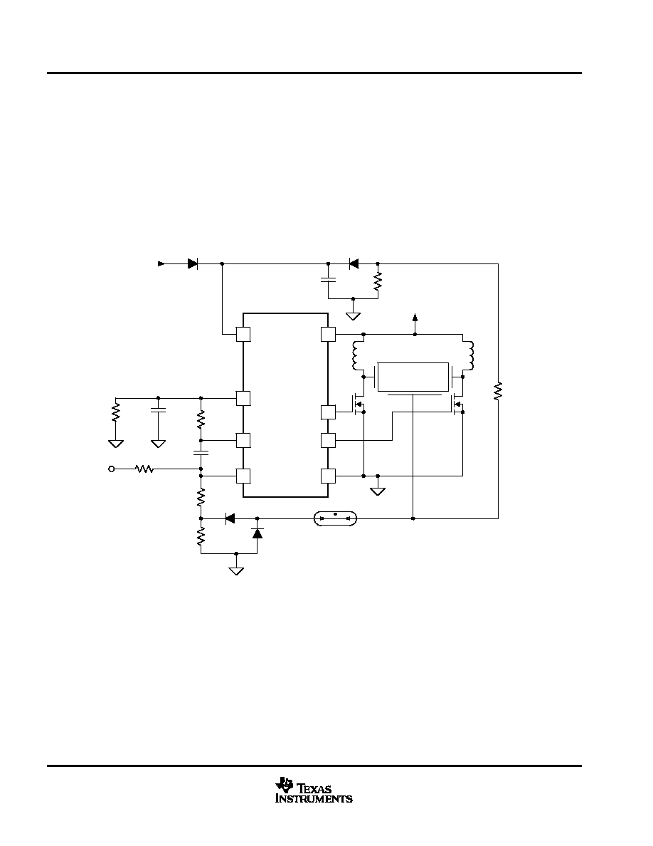
RANGE
1
3
2
4
8
6
7
5
OPEN/SD
OSC
COMP
FB
VDD
OUTP
OUTN
GND
CFB
RFB
DFB
CCFL
RCS
COSC
ROSC
LRES
PIEZO
XFMR
RHV
RCNT
VDD
COPEN
ROPEN
SHUTDOWN
UCC3976
DOPEN
UDG≠01092
Figure 1. UCC3976-Based CCFL Power Supply Using a Resonant Half-Bridge Topology
Copyright
2002, Texas Instruments Incorporated
PRODUCTION DATA information is current as of publication date.
Products conform to specifications per the terms of Texas Instruments
standard warranty. Production processing does not necessarily include
testing of all parameters.
UCC2975, UCC2976, UCC2977
UCC3975, UCC3976, UCC3977
SLUS499A ≠ NOVEMBER 2001 ≠ REVISED JANUARY 2002
2
www.ti.com
description (continued)
A half-bridge PZT converter, using the UCC3976 is shown in Figure 1. External P- and N-channel MOSFETs
are driven out of phase at a fixed 50% duty cycle with anti-cross conduction circuitry provided by the controller.
The half-bridge topology uses only a single magnetic component (LRES) reducing board area. As explained
in the applications section of this datasheet, regulation of lamp current is achieved by controlling the operating
frequency of the system.
The UCC3977 is designed to control a resonant push-pull topology as shown in Figure 2. This controller
alternately drives external N-channel MOSFETs at 50% duty cycle. The push-pull topology requires two external
inductors (L1 and L2), but has the advantage of providing increased voltage across the piezoelectric transformer
primary. In this case a small overlap is provided to the gate drives, assuring an uninterrupted path for inductor
current.
UDG≠01097
RANGE
1
3
2
4
8
6
7
5
OPEN/SD
OSC
COMP
FB
VDD
OUT1
OUT2
GND
CFB
RFB
DFB
CCFL
RCS
COSC
ROSC
RHV
RCNT
VDD
COPEN
ROPEN
DOPEN
SHUTDOWN
UCC3977
L1
PIEZO XFMR
N1
N2
L2
VCNT
Figure 2. UCC3977 Based CCFL Power Supply Using a Resonant Push-Pull Topology
For piezoelectric transformer applications requiring additional gain, a resonant flyback topology can be
implemented using the UCC3975. As shown in Figure 3, a magnetic transformer (T1) provides a stepped up
voltage to the piezoelectric transformer primary. When compared to a traditional high-voltage transformer used
in a CCFL application, T1 is small and low profile because of its reduced turns ratio and voltage rating. In the
resonant flyback application, a single switch is driven at 50% duty cycle producing a half wave rectified sinusoid
at the piezoelectric transformer primary.

UCC2975, UCC2976, UCC2977
UCC3975, UCC3976, UCC3977
SLUS499A ≠ NOVEMBER 2001 ≠ REVISED JANUARY 2002
3
www.ti.com
description (continued)
UDG≠01098
RANGE
1
3
2
4
8
6
7
5
OPEN/SD
OSC
COMP
FB
VDD
OUTP
OUTN
GND
CFB
RFB
DFB
CCFL
RCS
COSC
ROSC
RHV
RCNT
VDD
COPEN
ROPEN
SHUTDOWN
UCC3975
N
VCNT
PIEZO
XFMR
Figure 3. UCC3975-Based CCFL Power Supply Using a Resonant Flyback Topology
absolute maximum ratings over operating free-air temperature (unless otherwise noted)
Supply voltage
VDD
15 V
. . . . . . . . . . . . . . . . . . . . . . . . . . . . . . . . . . . . . . . . . . . . . . . . . . . . . . . . . . . . . . . . . .
Input voltage
OPEN/SD, OSC, COMP, FB, VDD, OUTP
GND≠0.5 V to V
DD
+0.5 V
. . . . . . . . . . . . . .
Storage temperature range, T
stg
≠65
į
C to 150
į
C
. . . . . . . . . . . . . . . . . . . . . . . . . . . . . . . . . . . . . . . . . . . . . . . . . . . .
Junction temperature range, T
J
≠40
į
C to 125
į
C
. . . . . . . . . . . . . . . . . . . . . . . . . . . . . . . . . . . . . . . . . . . . . . . . . . . .
Lead temperature 1,6 mm (1/16 inch) from case for 10 seconds
300
į
C
. . . . . . . . . . . . . . . . . . . . . . . . . . . . . . . .
Stresses beyond those listed under "absolute maximum ratings" may cause permanent damage to the device. These are stress ratings only, and
functional operation of the device at these or any other conditions beyond those indicated under "recommended operating conditions" is not
implied. Exposure to absolute-maximum-rated conditions for extended periods may affect device reliability.
ß All voltages are respect to GND.
AVAILABLE OPTIONS
PACKAGED DEVICES TSSOP (PW)
TA
TOPOLOGY
TA
FLYBACK
HALF-BRIDGE
PUSH-PULL
≠40
į
C to 85
į
C
UCC2975PW
UCC2976PW
UCC2977PW
0
į
C to 70
į
C
UCC3975PW
UCC3976PW
UCC3977PW
The PW package is available taped and reeled. Add TR suffix to device type
(e.g. UCC2975TRPW) to order quantities of 2500 devices per reel.
UCC2975, UCC2976, UCC2977
UCC3975, UCC3976, UCC3977
SLUS499A ≠ NOVEMBER 2001 ≠ REVISED JANUARY 2002
4
www.ti.com
electrical characteristics V
DD
= 3 V to 13.5 V, T
A
= 0
į
C to 70
į
C for UCC3975/UCC3976/UCC3977,
T
A
= ≠40
į
C to 85
į
C for the UCC2975/UCC2976/UCC2977, T
A
= T
J
(unless otherwise noted)
input supply
PARAMETER
TEST CONDITIONS
MIN
TYP
MAX
UNITS
VDD supply current
Normal, VDD = 12 V
1
2.5
mA
VDD supply current
Shutdown
20
100
Ķ
A
VDD UVLO (turn-on) threshold voltage
2.70
2.85
3.00
V
UVLO hysteresis
100
200
300
mV
output
PARAMETER
TEST CONDITIONS
MIN
TYP
MAX
UNITS
P≠channel driver output voltage, VOUTP
IPIN = 100 mA,
Driving logic low
0.5
0.9
P-channel driver output voltage, (VDD ≠ VOUTP)
IPIN = ≠100 mA,
Driving logic high
0.5
0.9
Low-level N≠channel driver output voltage, VOUTN
IPIN = 100 mA,
Driving logic low
0.5
0.9
V
High-level N≠channel driver output voltage,
(VDD ≠ VOUTN)
IPIN = ≠100 mA,
Driving logic high
0.5
0.9
Rise time
VDD = 5 V,
CL = 1 nF,
200
Fall time
VDD = 5 V,
CL = 1 nF,
See Note 1
200
ns
Dead (overlap) time
See Note 1
250
ns
oscillator
PARAMETER
TEST CONDITIONS
MIN
TYP
MAX
UNITS
Upper threshold voltage
1.6
1.7
1.8
V
Lower threshold voltage
0.65
0.70
0.80
V
Frequency
ROSC = 24 k
, COSC = 470 pF
95
100
105
kHz
error amplifier
PARAMETER
TEST CONDITIONS
MIN
TYP
MAX
UNITS
Input voltage
1.465
1.500
1.535
V
Line regulation voltage
3 V
VDD
13.5 V
≠2
2
6
mV
Input bias current
≠500
≠100
nA
Open loop gain
0.5 V
COMP
3.0V,
See Note 1
60
80
dB
Low-level output voltage
FB = 2 V,
OPEN/SD = 1 V
ICOMP = 0.23 mA
0.08
0.15
V
FB = 1 V,
COMP = 2 V
1.5
5.0
mA
Output source current
FB = 1 V,
COMP = 2 V,
OPEN/SD = 3 V
≠10
10
Ķ
A
FB = 2 V,
COMP = 2 V
2.5
4.5
6
mA
Output sink current
FB = 2 V,
COMP = 2 V,
OPEN/SD = 3 V
≠10
10
Ķ
A
Unity gain bandwidth frequency
TJ = 25
į
C,
See Note 1
2
MHz
NOTE: 1. Ensured by design. Not production tested.

UCC2975, UCC2976, UCC2977
UCC3975, UCC3976, UCC3977
SLUS499A ≠ NOVEMBER 2001 ≠ REVISED JANUARY 2002
5
www.ti.com
electrical characteristics V
DD
= 3 V to 13.5 V, T
A
= 0
į
C to 70
į
C for UCC3975/UCC3976/UCC3977,
T
A
= ≠40
į
C to 85
į
C for the UCC2975/UCC2976/UCC2977, T
A
= T
J
(unless otherwise noted)
mode select
PARAMETER
TEST CONDITIONS
MIN
TYP
MAX
UNITS
Shutdown threshold voltage
2.45
2.50
2.65
Restart threshold voltage
0.3
0.5
0.7
Open lamp detect enable threshold voltage
UCC2975
UCC2976
UCC2977
1.3
1.5
1.6
V
Open lamp detect enable threshold voltage
UCC3975
UCC3976
UCC3977
1.4
1.5
1.6
V
MODE pull-down current
200
250
300
mA
No lock threshold voltage
2.4
2.5
2.6
V
functional block diagram
The UCC397x family of controllers contain an error amplifier whose output is preconditioned at startup, a
precision window comparator used to form the VCO, and dual MOSFET drivers customized for half-bridge or
push-pull operation. The part includes a frequency lock retry circuit, low current shutdown, and open lamp fault
protection.
UDG≠01053
Figure 4
OPEN/SD
+
2.5 V
+
0.5 V
+
1.5 V
S
Q
Q
R
SLEEP
PWRUP
SHUT DOWN
RESET
OPEN LAMP
PWRUP
FAULT
INIT
OSC
COMP
FB
+
FAULT
COUNTER
RESET
COUNT
FAULT
SLEEP
NO LOCK
S
Q
R
INIT
SLEEP
REF
UVLO
+
2.5 V
0.1 V
+
INIT
ERROR
AMPLIFIER
1.5 V
1.4 V
1.5 V
+
1.7 V
+
0.7 V
S
Q
R
1.75 V
D
Q
Q
CK
DEADTIME/OVERLAP
TIME
GENERA
T
O
R
GND
OUTN/OUT2
OUTP/OUT1
VDD
SLEEP

UCC2975, UCC2976, UCC2977
UCC3975, UCC3976, UCC3977
SLUS499A ≠ NOVEMBER 2001 ≠ REVISED JANUARY 2002
6
www.ti.com
Terminal Functions
TERMINAL
NO.
NAME
UCCx975
UCCx976
UCCx977
I/O
DESCRIPTION
COMP
3
O
Output of the error amplifier and control voltage used to set the VCO frequency
FB
4
I
Inverting input to the error amplifier
GND
5
O
Ground reference for the device
OPEN/SD
1
I
Open lamp protection and a low power shut down
OSC
2
I
Common connection point for components that control the frequency range for the voltage con-
trolled oscillator (VCO)
OUTP/OUT1
7
O
Output of an internal CMOS driver used to drive an N-channel MOSFET (for UCC3977), or a
P-channel MOSFET (for UCC3976) left open for UCC3975
OUTN/OUT2
6
O
Output of an internal CMOS driver used to drive an N-channel MOSFET.
VDD
8
O
Connects to the battery or system voltage
1
2
3
4
8
7
6
5
OPEN/SD
OSC
COMP
FB
VDD
OUTP
OUTN
GND
UCC2975, UCC2976
UCC3975, UCC3976
PW PACKAGE
(TOP VIEW)
1
2
3
4
8
7
6
5
OPEN/SD
OSC
COMP
FB
VDD
OUT1
OUT2
GND
UCC2977, UCC3977
PW PACKAGE
(TOP VIEW)

UCC2975, UCC2976, UCC2977
UCC3975, UCC3976, UCC3977
SLUS499A ≠ NOVEMBER 2001 ≠ REVISED JANUARY 2002
7
www.ti.com
pin assignments
OPEN/SD: This dual-purpose pin provides open lamp protection and a low power shutdown capability for the
part. This pin can also be used to provide burst mode dimming explained in the applications section that follows.
open lamp function
During startup this pin is internally driven low setting the initial condition for the open lamp circuit. An
external peak detection circuit interfaces between this pin and the lamp. If the voltage at the pin exceeds
1.5 V, an open lamp is assumed and the part re-initiates a startup sequence up to 7 times. If the lamp fails
to strike after 7 tries, the device enters an error shutdown mode. An open lamp induced shutdown can be
cleared either by cycling power on the device or by pulling the pin above 2.5 V and then below 0.5 V.
shutdown function
The device is put into shutdown mode (15-
Ķ
A of typical quiescent current) by forcing the pin above 2.5 V.
When this pin is subsequently brought below 0.5 V, the device comes out of shutdown mode and initiates
a new startup cycle. This pin can be used to delay startup until the system voltage is sufficient to strike
and operate the piezoelectric transformer.
OSC: This pin is the common connection point for components that control the frequency range for the voltage
controlled oscillator (VCO). An external RC circuit connected from this pin to ground sets the center frequency
for the VCO, where a second resistor connected from this pin to the COMP pin sets the allowable frequency
range. A precision window comparator is used to keep the exponentially decaying ramp voltage at this pin
between 0.7 V and 1.7 V. When the voltage decays below 0.7 V, an internal pull-up circuit charges this pin to
1.7 V, the voltage is then allowed to decay to 0.7 V at a rate determined by the external components. Equations
are provided in the applications section to assist in determining the size of the external components to achieve
the desired frequency range.
COMP: This pin is the output of the error amplifier and control voltage used to set the VCO frequency. During
startup internal switches precondition this output to 0 V producing the maximum frequency of operation. The
error amplifier is then allowed to slew its output voltage until the lamp strikes and lamp current is regulated. The
slew rate is set by the external feedback components. If this pin reaches 2.5 V, regulation was not achieved and
startup will be re≠initiated up to 7 times.
FB: This is the inverting input to the error amplifier. This input is compared to 1.5 V and is used to control lamp
current.
OUTP/OUT1: This pin is the output of an internal CMOS driver used to drive an N-channel MOSFET in the case
of the UCC3977 or a P-channel MOSFET in the case of the UCC3976. This pin is low slightly less than 50%
duty cycle in the case of the UCC3976 to prevent cross-conduction and is high slightly more than 50% duty cycle
in the case of the UCC3977 to provide overlap. This pin is left open for the UCC3975.
OUTN/OUT2: This pin is the output of an internal CMOS driver used to drive an N-channel MOSFET in the case
of the UCC3975 and UCC3976 or the second N-channel MOSFET in the case of the UCC3977. This pin is high
slightly less than 50% duty cycle in the case of the UCC3975 and UCC3976. The pin is high slightly more than
50% duty cycle in the case of the UCC3977 to provide overlap.
VDD: This pin connects to the battery or system voltage. This pin should be bypassed with a minimum of 0.1-
Ķ
F
of capacitance directly at the device , with an additional 5-
Ķ
F to 10-
Ķ
F low ESR bulk capacitor (ceramic is
preferred).
GND: Ground reference for the device. This pin should be used as the common ground point for power and
signal level ground traces.

UCC2975, UCC2976, UCC2977
UCC3975, UCC3976, UCC3977
SLUS499A ≠ NOVEMBER 2001 ≠ REVISED JANUARY 2002
8
www.ti.com
state diagram
A logic state diagram for the UCC397x family of controllers is shown in Figure 5. During power-up the controller
transitions from UVLO to the momentary startup state. During startup, the COMP pin is preconditioned at
maximum frequency and the OPEN/SD capacitor is discharged before beginning normal operation. In the
normal operating state, the frequency is swept from high to low allowing the lamp to be struck and the current
in the lamp to be regulated.
STARTUP *
OPEN/SD = 0V
COMP = 0V
OSC, OUT active
NORMAL OPERATION
OPEN/SD < 1.5V
COMP < 2.5V
OSC, OUT active
OPEN LAMP *
1.5V < OPEN/SD <2.5V
COMP < 2.5V
OSC, OUT active
NO≠LOCK *
COMP > 2.5V
OPEN/SD < 1.5V
OSC, OUT active
COUNT=7?
ERROR
SHUTDOWN
OSC active
OUT off state
UVLO
VDD < 3.0V
OSC inactive
OUT off state
COUNT=0
SHUTDOWN
OPEN/SD > 2.5V
COUNT =0
OSC inactive
OUT off state
Low current VDD,
OPEN/SD
VDD>3.0V
OPEN/SD
< 0.5V
NO
YES
Increment COUNT
OUT off state
UCC3975: OUT1 low, OUT2 low
UCC3976: OUTP high, OUTN high
UCC3977: OUT1 low, OUT2 low
* Momentary states
UDG≠01102
Figure 5. State Diagram
The normal operating state can be exited in one of four ways:
∑
bringing V
DD
< 3 V
∑
a user commanded shutdown (OPEN/SD > 2.5 V)
∑
an open lamp condition (OPEN/SD > 1.5 V), or
∑
if the device fails to achieve regulation before reaching minimum frequency (EAO > 2.5 V).
The latter two conditions cause an internal retry counter to increment before attempting another startup. If the
application does not operate normally after seven retrys, the controller enters an error induced shutdown state
removing power to the load. The error state and counter can be cleared by removing V
DD
to the part or by a
user commanded shutdown.

UCC2975, UCC2976, UCC2977
UCC3975, UCC3976, UCC3977
SLUS499A ≠ NOVEMBER 2001 ≠ REVISED JANUARY 2002
9
www.ti.com
APPLICATION INFORMATION
PZT operation
Ceramic piezoelectric transformers were first proposed by C.A. Rosen in 1956. Unlike magnetic transformers
that rely on electromagnetic energy transfer, PZTs transfer electric potential to mechanical force as shown in
Figure 6. The electrical-to-mechanical conversion of energy is referred to as the reverse piezoelectric effect
whereas the mechanical-to-electrical energy conversion is referred to as the direct piezoelectric effect.
+
ELECTRIC
POTENTIAL
ELECTRIC
POTENTIAL
MECHANICAL
FORCE
MECHANICAL
FORCE
+
UDG≠01099
Figure 6. Piezoelectric Effect
Each manufacturer has a unique recipe of materials and structural layering that determine their PZT's operating
characteristics. Common materials used to make PZTs include lead zirconate, lead titanate and lithium niobate.
Single layer PZTs are less costly and easier to manufacture, but have a lower voltage gain (typically 5 to 10 )
and may require a step-up magnetic transformer in order to operate the lamp. Multi-layered PZT designs are
more difficult to manufacture, but have a higher voltage gain (20 to 70) allowing a CCFL to be driven using
conventional off-the-shelf inductors.

UCC2975, UCC2976, UCC2977
UCC3975, UCC3976, UCC3977
SLUS499A ≠ NOVEMBER 2001 ≠ REVISED JANUARY 2002
10
www.ti.com
APPLICATION INFORMATION
MECHANICAL
DISPLACEMENT
MECHANICAL
STRESS
0
0
VIN
VOUT
SUPPORTS
L = LENGTH
T = THICKNESS
h = HEIGHT
FORCE
FORCE
PRIMARY
SECONDARY
UDG≠01076
Figure 7. Typical Longitudinal Mode Piezoelectric Transformer for CCFL Applications.
A typical multi-layer PZT with longitudinal mode geometry is shown in Figure 7, a single layer design would have
similar construction without the layering on the primary. An ac voltage is applied to the V
IN
electrodes causing
mechanical expansion and compression in the thickness direction (see Figure 6). This displacement on the
primary is transferred as a force in the longitudinal direction. Supports at
ľ
and
ĺ
wavelength provide a means
for a standing wave to be generated at a resonant frequency as shown. Mechanical resonance occurs at
multiple standing wave frequencies (n) based on the transformer's length and material velocity (v).
f
n
+
n
v
2
length
Voltage gain is a function of the PZT material coefficient g[
], the number of primary layers, the thickness of
the material and the overall length as follows:
V
GAIN
+
length
layers
thickness
g[
w
]
An electrode at V
OUT
is used to recover the amplified electrical potential at the secondary.
PZT electrical model
In order to predict PZT performance in a system, it is useful to develop an electrical circuit model. The model
shown in Figure 8 is often used to describe the behavior of a PZT near the fundamental resonant frequency.
Many PZT manufacturers will provide component values for the model based on measurements taken at
various frequencies and output loads.
(1)
(2)

UCC2975, UCC2976, UCC2977
UCC3975, UCC3976, UCC3977
SLUS499A ≠ NOVEMBER 2001 ≠ REVISED JANUARY 2002
11
www.ti.com
APPLICATION INFORMATION
L
C
R
1 : n
VIN
CINPUT
COUT VOUT
RLOAD
UDG≠01100
Figure 8. Equivalent Piezoelectric Transformer Circuit Model
The component values depend on the PZT's construction. A large primary capacitance (C
INPUT
) is formed as
a result of the multi-layer construction of the primary electrodes and material dielectric constant. The output
capacitance is much smaller due to the distance between the primary and secondary electrodes. Typical values
of C
INPUT
and C
OUT
for a multi≠layer PZT may be 0.2
Ķ
F and 20 pF respectively, where a single layer design
would have lower C
INPUT
since layers =1.
C
INPUT
+
length
width
layers
Ś
2
thickness
C
OUTPUT
+
2
thickness
width
Ś
length
C
INPUT
and an external transformer or inductor(s) are used to form a primary-side L-C resonant circuit as
depicted in Figures 1, 2 and 3. These circuits provide sinusoidal waveforms at the primary, allowing the PZT
to operate at higher efficiency. The mechanical resonant frequency (
0
) of the PZT (which differs from the
natural primary L-C resonant frequency) is proportional to the material elasticity (Y), density (
) and length.
w
0
T
1
length
Y
Ú
The mechanical piezoelectric gain near a single resonant frequency can modeled by a series R, L, and C circuit
as depicted in Figure 8.
w
0
+
1
L
C
Q
+ w
0
L
R
Figure 9 illustrates the gain-vs-output load and frequency characteristics for a 12-layer, 70-kHz PZT with the
following Figure 8 values:
∑
C
INPUT
= 0.2
Ķ
F
∑
C
OUT
= 30 pF
∑
n = 30
∑
series RLC (2
, 1
Ķ
H, 6 nF)
As shown in Figure 9, the ceramic transformer provides high Q and gain under light or no-load conditions
producing a high-strike potential. Once the lamp strikes the transformer becomes loaded, causing the
transformer gain to decrease and resonant frequency to shift. The piezoelectric transformer is typically operated
on the right side of resonance to allow the lamp to be struck and operated with a single direction control circuit.
A typical application has separate start (A), strike (B), and operating (C) frequencies (see Figure 9).
(3)
(4)
(5)
(6)
(7)

UCC2975, UCC2976, UCC2977
UCC3975, UCC3976, UCC3977
SLUS499A ≠ NOVEMBER 2001 ≠ REVISED JANUARY 2002
12
www.ti.com
APPLICATION INFORMATION
lamp characteristics
A cold cathode fluorescent lamp has non-linear V-I characteristics as shown in Figure 10. The lamp's intensity
(lumens) is roughly proportional to lamp current where lamp voltage remains somewhat constant over the
operating range. Lamp voltage is dependant on the diameter and length of the lamp used in the application. This
results in increased impedance when the lamp is dimmed. The impedance of the lamp will influence the gain
of the piezoelectric transformer (see Figure 9) and thus the operating frequency of the system.
start
Figure 9
60
65
70
75
80
50
0
150
100
200
300
250
ROUT = 500 k
ROUT = 250 k
ROUT = 100 k
ROUT = 750 k
f ≠ Frequency ≠ kHz
V
GAIN
≠
Gain
≠
V
PIEZOELECTRIC GAIN
vs
FREQUENCY
strike
A
C
B
operate
Figure 10
550
500
650
600
700
800
750
500
0
1500
1000
2000
3000
2500
0
1
2
3
4
5
6
Impedance
≠
k
V
LAMP
≠
Lamp V
o
ltage
≠
V
CCFL CURRENT
vs
LAMP VOLTAGE AND IMPEDANCE
ILAMP ≠ Lamp Current ≠ mA
LAMP
VOLTAGE
LAMP
IMPEDANCE
variable frequency control system
A simplified block diagram of a PZT based backlight converter is shown in Figure 11. The PZT is driven by a
resonant power stage whose amplitude is proportional to input voltage. The PZT then provides the voltage gain
necessary to drive the lamp. A control loop is formed around the error amplifier that compares average lamp
current to a reference signal (REF) allowing the intensity of the lamp to be regulated. The resulting control
voltage V
C
drives a VCO that determines the operating frequency of the resonant power stage.
The frequency range of the VCO must include the strike and operating frequencies of the PZT with some
tolerance included for component variation. Minimizing the programmable range improves the control response
of the feedback loop. For example, a frequency range of 67 kHz to 77 kHz might be used for the PZT in Figure 9.
The gain of the PZT must guarantee sufficient lamp voltage at minimum input voltage to ensure that the control
loop will always operate on the right side of resonance.

UCC2975, UCC2976, UCC2977
UCC3975, UCC3976, UCC3977
SLUS499A ≠ NOVEMBER 2001 ≠ REVISED JANUARY 2002
13
www.ti.com
APPLICATION INFORMATION
+
≠
RESONANT
POWER
STAGE
DC INPUT
VOLTAGE
VOLTAGE
CONTROLLED
OSCILLATOR
REF
CCFL
LAMP CURRENT
SENSE
ERROR
AMPLIFIER
PIEZOELECTRIC
TRANSFORMER
VC
UDG≠01101
Figure 11. Control System for Variable Frequency PZT Backlight Control
programming the frequency range
The frequency range of the UCC397x family is programmed with external components R
OSC
, C
OSC
, and R
ANGE
(see Figures 2 and 3). The programmed range should include the strike and operating frequency required for
lamp operation, plus sufficient tolerance for component variations. An accurate NPO capacitor is recommended
for C
OSC
(between 100 pF and 1000 pF) while 1% resistors are recommended for R
OSC
and R
ANGE
. The VCO
frequency is determined by the charge and decay times between 0.7 V and 1.7 V at the OSC pin. When the
voltage reaches 0.7 V, an internal pull-up circuit charges OSC back to 1.7 V, the charge time (t
CHG
) varies with
the value of C
OSC
but is typically on the order of 500 ns. The decay time (t
DISCH
) is determined by the value
of C
OSC
and the discharge currents generated in R
OSC
and R
ANGE
. The nominal discharge time at OSC is set
by R
OSC
and C
OSC
(see equation [8]), the frequency range is programmed by adjusting the discharge time with
the R
ANGE
resistor and the COMP voltage (see equation [9]):
nominal
t
DISCH
+
R
OSC
C
OSC
ln 1.7
0.7
with lamp
t
DISCH
V
COMP
+
R
OSC
R
ANGE
C
OSC
R
OSC
)
R
ANGE
ln
1.7 R
OSC
)
R
ANGE
*
V
COMP
R
OSC
0.7 R
OSC
)
R
ANGE
*
V
COMP
R
OSC
resulting frequency
Frequency V
COMP
+
1
t
CHG
)
t
DISCH
V
COMP
(8)
(9)
(10)

UCC2975, UCC2976, UCC2977
UCC3975, UCC3976, UCC3977
SLUS499A ≠ NOVEMBER 2001 ≠ REVISED JANUARY 2002
14
www.ti.com
APPLICATION INFORMATION
Equations 8 and 9 are derived by solving Laplace or differential equations for the RC decay time from 1.7 V to
0.7 V with and without the effect of V
COMP
. The resulting frequency of the system is given in equation 10. This
frequency should be verified in the lab and may need adjustment depending on factors such as extra
capacitance at the OSC pin (oscilloscope measurements can affect frequency) as well as noise. Figure 12
shows the resulting frequency-to-control voltage relationship with the component values listed below the figure
and a t
CHG
time of 500 ns.
Figure 12
f OSC
≠
Oscillator Frequency
≠
kHz
ERROR AMPLIFIER VOLTAGE
vs
OSCILLATOR FREQUENCY
VCOMP ≠ Error Amplifier Voltage ≠ V
0
0.5
1.0
1.5
2.0
2.5
62
60
70
64
74
80
76
68
66
78
72
ROSC = 15.8 k
COSC = 560 pF
RANGE = 162 k

UCC2975, UCC2976, UCC2977
UCC3975, UCC3976, UCC3977
SLUS499A ≠ NOVEMBER 2001 ≠ REVISED JANUARY 2002
15
www.ti.com
APPLICATION INFORMATION
setting lamp current
The lamp current is controlled by adjusting the frequency of the PZT. System frequency and lamp current control
is accomplished through the error amplifier (EA) and the voltage controlled oscillator (VCO) as shown in
Figure 12. Lamp current is sensed at RCS and is averaged at EA≠ by RFB and CFB.
V
CS
+
I
LAMP
RCS
2
p
Equation (11) assumes the error amplifier loop is closed, the relationship between V
CS
and V
CNT
(dimming
control voltage) is given in equation (4).
1.5 V
+
V
CNT
R
FB
)
V
CNT
R
CNT
R
FB
)
R
CNT
The relationship between control voltage and lamp current can be easily programmed for the application. For
example suppose maximum lamp current is 5 mA (V
CNT
= 0 V) and minimum lamp current is 1 mA
(V
CNT
= 3 V). R
CS
is calculated to be 1100
by using equation (12) and setting the lamp current to 3 mA
(V
CNT
= 1.5 V, V
CS
= 1.5 V). R
CNT
is calculated to be 150 k
by selecting R
FB
at 100 k
and solving equation
(12) at maximum lamp current (V
CNT
= 0 V, I
LAMP
= 5 mA). Using these, the resulting control voltage to lamp
current equation becomes:
I
LAMP
+
3.75
*
V
CNT
742
∑
R
CS
= 1100
∑
R
CNT
= 150 k
∑
R
FB
= 100 k
sizing the feedback capacitor
Feedback design with a PZT requires both modeling and measurement. The uncompensated feedback gain
for the system is primarily affected by the gain slope of the PZT near its resonant operating frequency as shown
in Figure 9. For most designs, the safe unity gain crossover frequency of the feedback loop will be determined
by the amount of gain peaking that occurs at the resonant frequency of the PZT transformer. R
FB
and C
FB
are
selected to have a fairly low crossover frequency to ensure that the system gain does not increase above unity
at the resonant switching frequency. Since the gain slope is dependant on the lamp load and PZT model, it is
recommended that a network analyzer is used to validate sufficient gain and phase margin for the design.
A simple first order (or integral) feedback stage is used to stabilize the feedback response of the system.
Selection of the feedback capacitor (C
FB
) and resistor (R
FB
) is primarily dependant upon the small signal gain
of the system and the desired sweep rate of the VCO. If the frequency is swept too rapidly at startup (with an
undersized C
FB
), the feedback loop will not stabilize after the lamp is struck and the controller will cycle through
the VCO frequency range without locking. A feedback capacitor that is too large has poor transient performance.
A C
FB
value of 0.1
Ķ
F is usually a good starting point for most designs if R
FB
is 100 k
. With analog dimming,
the C
FB
value must be large enough to be stable at high V
IN
and minimum lamp current (maximum PZT gain
slope and load). The C
FB
value can be decreased with burst dimming since the lamp is operated at full load
where the PZT gain slope is reduced.
(11)
(12)
(13)

UCC2975, UCC2976, UCC2977
UCC3975, UCC3976, UCC3977
SLUS499A ≠ NOVEMBER 2001 ≠ REVISED JANUARY 2002
16
www.ti.com
APPLICATION INFORMATION
matching the PZT to the lamp, input voltage and topology
A fundamental challenge in the design of a piezoelectric transformer-based CCFL application is to match the
lamp's power requirements with the transformer. Since the piezoelectric transformer is a mechanical system,
the energy delivered by the transformer is a function of its mass and its vibrational velocity (
).
energy
T
mass
n
2
The power delivered by the transformer is described in equation (15):
power
+
energy
d
dt
+
energy
frequency
The design challenge becomes how operate the transformer within its gain and power delivering capabilities
while optimizing overall system efficiency. This optimization requires knowledge of both the lamp and
piezoelectric transformer for the particular application. Achieving optimal efficiency with a given lamp and
piezoelectric transformer will require bench measurements and design iterations. There are several factors that
should be taken into consideration when selecting a piezoelectric transformer:
∑
What is the recommended input voltage for the PZT?
∑
What is the input capacitance of the PZT?
∑
What is the gain of the transformer at various load conditions? (see Figure 9)
∑
At what frequency does the PZT give maximum gain?
The recommended input voltage and gain of the piezoelectric transformer influence the power topology
selection. As mentioned earlier, the half-bridge topology gives the least gain where the push-pull topology
doubles the primary voltage. The flyback topology can provide additional gain through the flyback transformer.
The input capacitance and operating frequency of the piezoelectric transformer determines the required value
of the external inductor(s) (or transformer inductance in the case of the flyback). The external inductance value
may need to be further optimized to get the best performance.
(14)
(15)

UCC2975, UCC2976, UCC2977
UCC3975, UCC3976, UCC3977
SLUS499A ≠ NOVEMBER 2001 ≠ REVISED JANUARY 2002
17
www.ti.com
APPLICATION INFORMATION
half-bridge operation and inductor selection
In the half-bridge topology, the external inductor and piezoelectric capacitance form a low-pass filter between
the common switch node of the external MOSFETs and the piezoelectric primary as shown on the front page.
The L-C filter formed by these components should pass the resonant frequency, required by the piezoelectric
transformer, yet attenuate higher harmonic components. The choice of inductor will require bench
measurements and modeling of the resonant circuit:
∑
An inductor value that is too low (high L-C resonant frequency) will result in non-sinusoidal primary
waveforms since higher order harmonics are allowed though the filter. A low value also allows excess
circulating currents, impacting efficiency.
∑
An inductor value that results in a L-C resonant frequency close to the resonant frequency of the
piezoelectric transformer causes interference, making control of the primary voltage difficult. The
interference occurs since the gain of the L-C tank depends heavily on load in this region of operation.
∑
An inductor value that is too large causes an attenuation of the input voltage, increasing the gain
requirements of the piezoelectric transformer and/or the system.
As an example, suppose a piezoelectric transformer is selected that operates efficiently at 67 kHz (similar to
Figure 9) and has 0.2-
Ķ
F of primary capacitance. An external inductance value of 15
Ķ
H gives a L-C filter corner
frequency of 92 kHz. The L-C circuit would provide little attenuation at 67 kHz yet attenuate higher harmonics.
Figure 13
f ≠ Frequency ≠ kHz
V
GAIN
≠
Gain
≠
V
UCC3976 L-C TANK FREQUENCY
vs
LAMP LOADS
0
50
150
200
250
300
100
0
1
1.5
2.0
0.5
fPZT = 67 kHz
LAMP LOAD
150 k
100 k
50 k

UCC2975, UCC2976, UCC2977
UCC3975, UCC3976, UCC3977
SLUS499A ≠ NOVEMBER 2001 ≠ REVISED JANUARY 2002
18
www.ti.com
APPLICATION INFORMATION
half-bridge operation and inductor selection (continued)
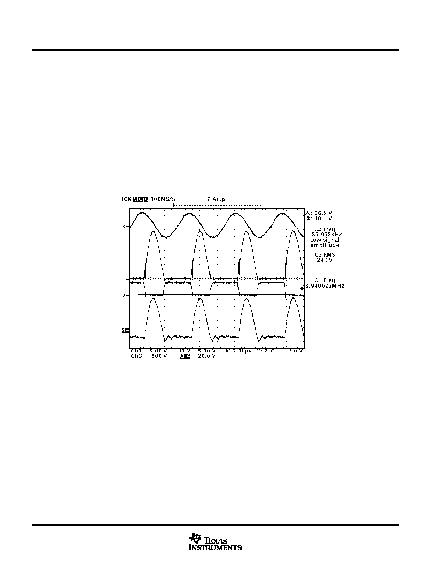
Waveforms for the UCC3976 half-bridge circuit operated with a 12-Vdc input are shown in Figure 14. P- and
N-Channel MOSFETs are driven out of phase with 50% duty cycle producing a square wave at the drains (see
Figure15: trace 1). Inductor LRES and the PZT primary capacitance form a low-pass filter. The resulting in a
near sinusoid across the PZT primary (trace 2). Due to the high Q of the PZT, lamp voltage (trace 4) is sinusoidal.
Lamp current is sensed by the half-wave rectification circuit at RCS (trace 3). Lamp current is in phase with lamp
current since the load is primarily resistive with some capacitance due to the reflector's proximity to the lamp.
The lamp reflector should be grounded for safety reasons and in order to keep the secondary capacitance
constant allowing the PZT load to be constant.
VIN = 12 Vdc
VLAMP = 600 V
Figure 14. UCC3976 Half-Bridge Waveforms

UCC2975, UCC2976, UCC2977
UCC3975, UCC3976, UCC3977
SLUS499A ≠ NOVEMBER 2001 ≠ REVISED JANUARY 2002
19
www.ti.com
APPLICATION INFORMATION
push-pull operation and inductor selection
For the push-pull circuit, MOSFETs N1 and N2 are driven out of phase with 50% duty cycle at variable frequency
(see Figure 15: trace 2). Inductors L1 and L2 resonate with the PZT primary capacitance, forming a half
sinusoids at the drain of N1 (trace 1) and S2 (trace 4). The resulting voltage across the PZT primary is a near
sinusoid (trace M1). Due to the high Q of the ceramic transformer, the lamp voltage, which is approximately
600 V in this application, is sinusoidal (trace 3). In order to achieve zero-voltage switching, each drain voltage
must return to zero before the next switching cycle. This dictates that the L-C resonant frequency be greater
than the switching frequency. The maximum inductance to meet these conditions can be found from
equation (16):
L
t
1
4
p
2
f
2
C
p
VIN = 7 Vdc
VLAMP = 600 V
Figure 15. UCC3977 Push-Pull Waveforms
(16)
UCC2975, UCC2976, UCC2977
UCC3975, UCC3976, UCC3977
SLUS499A ≠ NOVEMBER 2001 ≠ REVISED JANUARY 2002
20
www.ti.com
APPLICATION INFORMATION
flyback operation
For single layer PZT applications requiring additional gain, a resonant flyback topology can be implemented as
shown in Figure 16. In the resonant flyback application, a single N-channel switch is driven at 50% duty cycle
producing a half sinusoid at the drain (see Figure 16: trace 1). The magnetic transformer provides a stepped
up voltage to the PZT primary (trace 4). The resulting lamp voltage at the PZT secondary, which is approximately
250 V in this case, is sinusoidal resulting from the high Q of the ceramic transformer (trace 3). When compared
to a high-voltage magnetic CCFL transformer, the magnetic step-up transformer is small and low profile
because of the reduced turns ratio (3.5:1) and voltage rating. To ensure zero-voltage switching, as in the case
of the push-pull converter, equation (16) must be validated. The L-C relationship can be analyzed on either the
primary or secondary side of the magnetic transformer. If viewed from the primary, PZT capacitance is reflected
by the turns ratio.
VIN = 4 Vdc
VLAMP = 250 V
Figure 16. UCC3975 Resonant Flyback Waveforms

UCC2975, UCC2976, UCC2977
UCC3975, UCC3976, UCC3977
SLUS499A ≠ NOVEMBER 2001 ≠ REVISED JANUARY 2002
21
www.ti.com
APPLICATION INFORMATION
analog dimming PZT performance
High efficiency can be achieved by selecting the best power topology while matching the lamp, input voltage
and PZT characteristics. Figure 17 shows the performance of a 3-W rated multi-layer PZT operating a 600 V
lamp using the push-pull topology at various input voltage and lamp current conditions. Electrical efficiency is
greater than 85% at lower input voltages, decreasing at higher input voltages as the PZT gain is reduced. This
circuit and lamp can operate from 2 Li-Ion cells with voltages between 5 V and 8.2 V. The same PZT and lamp
would require three Li≠Ion cells for the half-bridge topology but would yield similar efficiency.
Dimming by linearly reducing lamp current causes the efficiency to degrade since the PZT is operated at less
than optimal gain (see 1.5 mA curve). Improved efficiency can be achieved by using burst mode dimming. This
dimming method involves running the lamp at full power, but controlling average lamp current by modulating
the on/off duty cycle at a frequency higher than the eye can detect (100 Hz, for example).
Figure 18 shows plots of PZT operating frequency over the same lamp conditions as Figure 17. As expected,
frequency decreases at higher lamp currents as the PZT characteristics shift to a lower operating frequency
when loaded (see Figure 2). Frequency increases linearly with input voltage, since the required V
OUT
/V
IN
gain
to operate the lamp is decreased.
Figure 17
TYPICAL PIEZO TRANSFORMER EFFICIENCY
vs
INPUT VOLTAGE
4
55
50
75
60
85
95
70
65
90
80
5
7
8
9
6
10
Efficiency
≠
%
VIN ≠ Input Voltage ≠ Vdc
1.5 mA
660 V
4.5 mA
570 V
3.0 mA
610 V
Figure 18
f OSC
≠
Oscillator Frequency
≠
kHz
PIEZO TRANSFORMER FREQUENCY
vs
INPUT VOLTAGE
4
60.5
60.0
62.5
61.0
63.5
64.5
62.0
61.5
64.0
63.0
65.0
5
7
8
9
6
10
VIN ≠ Input Voltage ≠ Vdc
4.5 mA
570 V
1.5 mA
570 V
3.0 mA
610 V

UCC2975, UCC2976, UCC2977
UCC3975, UCC3976, UCC3977
SLUS499A ≠ NOVEMBER 2001 ≠ REVISED JANUARY 2002
22
www.ti.com
APPLICATION INFORMATION
open lamp shutdown/no-lock operation
Due to the high gain characteristics of the piezoelectric transformer, it is important that the operation of the power
stage is suspended if an open lamp occurs. Figure 19 shows the output voltage of a piezoelectric transformer
with no output load and driven with a 5-V
RMS
sinusoid on the primary. The primary frequency is swept through
the resonant frequency of the piezoelectric transformer. As seen in Figure 19 the output voltage approaches
2 kV
RMS
with open lamp disabled, a gain of 400! If the input voltage were increased to 10 V
RMS
, the output would
reach 4 kV
RMS
and possibly crack the PZT transformer.
OPEN LAMP
PROTECTION
DISABLED
Maximum
Frequency
Minimum
Frequency
PZT Resonant
Frequency
Figure 19. Damaging Voltages at Piezoelectric Transformer Secondary
In order to prevent damaging voltages at the piezoelectric transformer secondary, a 1.5-V comparator at the
OPEN/SD pin is used to shutdown the converter if an open lamp is detected. The RMS secondary voltage at
which an open lamp fault is triggered can be calculated using equation (17).
V
OPEN
+
1.5
)
V
DIODE
R
HV
2
R
OPEN
R
HV
will typically consist of several inexpensive high impedance resistors to minimize current in the divider and
to stand≠off high voltage. R
HV
can be replaced with a single high voltage capacitor if component count is an
issue, however, impedance of the capacitor over frequency needs to be taken into consideration.
(17)
UCC2975, UCC2976, UCC2977
UCC3975, UCC3976, UCC3977
SLUS499A ≠ NOVEMBER 2001 ≠ REVISED JANUARY 2002
23
www.ti.com
APPLICATION INFORMATION
open lamp shutdown/no-lock operation (continued)
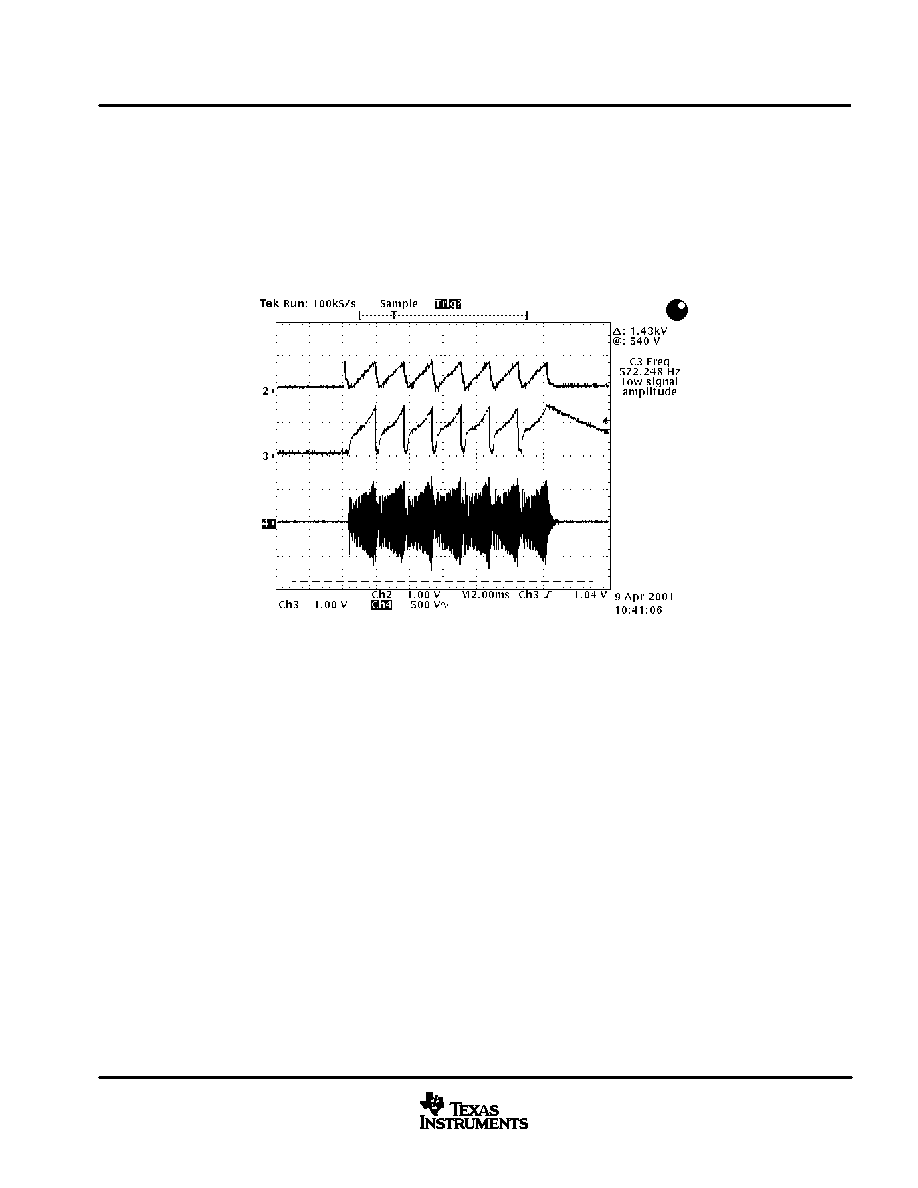
Figure 20 shows the startup performance of the UCC397x family based system with a broken or open lamp.
The open lamp trip level is typically set 20% to 50% higher than the required strike voltage of the lamp, in this
example the open lamp trip level is set at a low 500 V
RMS
. As seen in Figure 21, the lamp does not strike before
the OPEN/SD pin reaches 1.5 V indicating an open lamp, the controller retries seven times before entering an
error shutdown state (see the state diagram in the pin description section).
VCOMP
VOPEN/SD
VPZT
Figure 20. Start-Up With Open Lamp
A second type of failure mode occurs if the system fails to control lamp current. Assuming a proper feedback
network, this failure can occur if the input voltage is too low to operate the lamp or if one of the components in
the power path is open, shorted, or broken. These failures are detected at the COMP pin. Figure 21 shows the
system response where the input voltage is not sufficient for lamp operation. At startup the frequency sweeps
through the range until COMP reaches 2.5 V, the controller attempts seven retries before entering the error
shutdown state. Notice the slope on the COMP pin (trace 2) changes as the system attempts to operate the lamp
in a high gain region but is ultimately unsuccessful.

UCC2975, UCC2976, UCC2977
UCC3975, UCC3976, UCC3977
SLUS499A ≠ NOVEMBER 2001 ≠ REVISED JANUARY 2002
24
www.ti.com
APPLICATION INFORMATION
open lamp shutdown/no-lock operation (continued)
VCOMP
VOPEN/SD
VPZT
Figure 21. Start-Up With Insufficient Input Voltage

UCC2975, UCC2976, UCC2977
UCC3975, UCC3976, UCC3977
SLUS499A ≠ NOVEMBER 2001 ≠ REVISED JANUARY 2002
25
www.ti.com
APPLICATION INFORMATION
burst dimming with the OPEN/SD pin
A burst dimming technique can be used with CCFLs when a wide dimming range is required, this technique can
also yield better efficiency at light loads. Burst dimming is implemented by running the lamp at full current when
on, where the on/off duty factor is controlled a low frequency to provide dimming. In order to prevent visible
flicker, the burst frequency needs to be set higher than 80 Hz.
The UCC397x family is initially targeted for operating the PZT using analog dimming, however, burst dimming
can be implemented by controlling the OPEN/SD pin directly with a square wave. Figure 22 shows burst
dimming performance using the UCC3976 at 125 Hz and 50% duty cycle. In Figures 22≠25, trace 1 is the drain
connection of the external P- and N-Channel MOSFETs, trace 2 is the OPEN/SD pin which is externally driven
with a 5-V square wave, trace 3 is the COMP pin which is used to lock the operating frequency and trace 4 is
the lamp voltage. These scope graphics were captured with a digital oscilloscope, so aliasing is present in
Figures 22≠24. Referring back to Figure 22, when OPEN/SD is driven to 5 V the part is in shutdown and the
controller is disabled. When OPEN/SD is forced to 0 V by the external source the controller goes through its
startup sequence with COMP starting at 0 V allowing the PZT to strike the lamp and lock on the frequency
required to regulate the lamp at full current. The size of the feedback capacitor determines the slew rate at which
COMP can lock the system frequency which effects the achievable duty cycle of burst dimming. Fortunately,
the feedback cap with burst dimming can be smaller than with analog dimming since the system small signal
gain is lower at full lamp load. Figures 23 and 24 show burst dimming at approximately 10% and 90% duty cycle
respectively. Figure 25 shows a close up of the startup sequence when OPEN/SD is pulled low. COMP is
preconditioned to 0 V before switching begins and then allowed to ramp up. PZT secondary voltage ramps as
the frequency decreases until the lamp strikes and operates. Strike voltage for the lamp is barely detectable
since the lamp is warm and operating from the previous burst cycles.
VCOMP
VOPEN/SD
VLAMP
VOPEN/SD
Figure 22. UCC3976 Burst Dimming at 50% Duty Cycle
VIN = 12 Vdc
VLAMP = 600 V
fOSC = 125 Hz
50% Duty Cycle
ILAMP = 5 mA

UCC2975, UCC2976, UCC2977
UCC3975, UCC3976, UCC3977
SLUS499A ≠ NOVEMBER 2001 ≠ REVISED JANUARY 2002
26
www.ti.com
TYPICAL WAVEFORMS
VCOMP
VOPEN/SD
VLAMP
VOPEN/SD
VIN = 12 Vdc
VLAMP = 600 V
fOSC = 125 Hz
10% Duty Cycle
ILAMP = 5 mA
Figure 23. UCC3976 Externally Controlled Bursting Dimming
at 10% Duty Cycle
VCOMP
VOPEN/SD
VLAMP
VOPEN/SD
VIN = 12 Vdc
VLAMP = 600 V
fOSC = 125 Hz
90% Duty Cycle
ILAMP = 5 mA
Figure 24. UCC3976 Externally Controlled Bursting Dimming
at 90% Duty Cycle

UCC2975, UCC2976, UCC2977
UCC3975, UCC3976, UCC3977
SLUS499A ≠ NOVEMBER 2001 ≠ REVISED JANUARY 2002
27
www.ti.com
TYPICAL WAVEFORMS
VCOMP
VOPEN/SD
VLAMP
VIN = 12 Vdc
VLAMP = 600 V
fOSC = 125 Hz
10% Duty Cycle
ILAMP = 5 mA
VOPEN/SD
Figure 25. UCC3976 Close-Up of Bursting Dimming Operation
at 10% Duty Cycle

IMPORTANT NOTICE
Texas Instruments Incorporated and its subsidiaries (TI) reserve the right to make corrections, modifications,
enhancements, improvements, and other changes to its products and services at any time and to discontinue
any product or service without notice. Customers should obtain the latest relevant information before placing
orders and should verify that such information is current and complete. All products are sold subject to TI's terms
and conditions of sale supplied at the time of order acknowledgment.
TI warrants performance of its hardware products to the specifications applicable at the time of sale in
accordance with TI's standard warranty. Testing and other quality control techniques are used to the extent TI
deems necessary to support this warranty. Except where mandated by government requirements, testing of all
parameters of each product is not necessarily performed.
TI assumes no liability for applications assistance or customer product design. Customers are responsible for
their products and applications using TI components. To minimize the risks associated with customer products
and applications, customers should provide adequate design and operating safeguards.
TI does not warrant or represent that any license, either express or implied, is granted under any TI patent right,
copyright, mask work right, or other TI intellectual property right relating to any combination, machine, or process
in which TI products or services are used. Information published by TI regarding third≠party products or services
does not constitute a license from TI to use such products or services or a warranty or endorsement thereof.
Use of such information may require a license from a third party under the patents or other intellectual property
of the third party, or a license from TI under the patents or other intellectual property of TI.
Reproduction of information in TI data books or data sheets is permissible only if reproduction is without
alteration and is accompanied by all associated warranties, conditions, limitations, and notices. Reproduction
of this information with alteration is an unfair and deceptive business practice. TI is not responsible or liable for
such altered documentation.
Resale of TI products or services with statements different from or beyond the parameters stated by TI for that
product or service voids all express and any implied warranties for the associated TI product or service and
is an unfair and deceptive business practice. TI is not responsible or liable for any such statements.
Mailing Address:
Texas Instruments
Post Office Box 655303
Dallas, Texas 75265
Copyright
2001, Texas Instruments Incorporated