Äîêóìåíòàöèÿ è îïèñàíèÿ www.docs.chipfind.ru

TSB43AB22A
Integrated 1394a 2000 OHCI PHY/Link Layer
Controller
December 2001
1394 Host Controller Solutions
Data Manual
SLLS520

IMPORTANT NOTICE
Texas Instruments and its subsidiaries (TI) reserve the right to make changes to their products or to discontinue
any product or service without notice, and advise customers to obtain the latest version of relevant information
to verify, before placing orders, that information being relied on is current and complete. All products are sold
subject to the terms and conditions of sale supplied at the time of order acknowledgment, including those
pertaining to warranty, patent infringement, and limitation of liability.
TI warrants performance of its products to the specifications applicable at the time of sale in accordance with
TI's standard warranty. Testing and other quality control techniques are utilized to the extent TI deems necessary
to support this warranty. Specific testing of all parameters of each device is not necessarily performed, except
those mandated by government requirements.
Customers are responsible for their applications using TI components.
In order to minimize risks associated with the customer's applications, adequate design and operating
safeguards must be provided by the customer to minimize inherent or procedural hazards.
TI assumes no liability for applications assistance or customer product design. TI does not warrant or represent
that any license, either express or implied, is granted under any patent right, copyright, mask work right, or other
intellectual property right of TI covering or relating to any combination, machine, or process in which such
products or services might be or are used. TI's publication of information regarding any third party's products
or services does not constitute TI's approval, license, warranty or endorsement thereof.
Reproduction of information in TI data books or data sheets is permissible only if reproduction is without
alteration and is accompanied by all associated warranties, conditions, limitations and notices. Representation
or reproduction of this information with alteration voids all warranties provided for an associated TI product or
service, is an unfair and deceptive business practice, and TI is not responsible nor liable for any such use.
Resale of TI's products or services with statements different from or beyond the parameters stated by TI for
that product or service voids all express and any implied warranties for the associated TI product or service,
is an unfair and deceptive business practice, and TI is not responsible nor liable for any such use.
Also see: Standard Terms and Conditions of Sale for Semiconductor Products. www.ti.com/sc/docs/stdterms.htm
Mailing Address:
Texas Instruments
Post Office Box 655303
Dallas, Texas 75265
Copyright
2001, Texas Instruments Incorporated

iii
Contents
Section
Title
Page
1
Introduction
11
. . . . . . . . . . . . . . . . . . . . . . . . . . . . . . . . . . . . . . . . . . . . . . . . . . . . . .
1.1
Description
11
. . . . . . . . . . . . . . . . . . . . . . . . . . . . . . . . . . . . . . . . . . . . . . . . .
1.2
Features
13
. . . . . . . . . . . . . . . . . . . . . . . . . . . . . . . . . . . . . . . . . . . . . . . . . . .
1.3
Related Documents
14
. . . . . . . . . . . . . . . . . . . . . . . . . . . . . . . . . . . . . . . . . .
1.4
Trademarks
14
. . . . . . . . . . . . . . . . . . . . . . . . . . . . . . . . . . . . . . . . . . . . . . . . .
1.5
Ordering Information
14
. . . . . . . . . . . . . . . . . . . . . . . . . . . . . . . . . . . . . . . . .
2
Terminal Descriptions
21
. . . . . . . . . . . . . . . . . . . . . . . . . . . . . . . . . . . . . . . . . . . . .
3
TSB43AB22A 1394 OHCI Controller Programming Model
31
. . . . . . . . . . . .
3.1
PCI Configuration Registers
33
. . . . . . . . . . . . . . . . . . . . . . . . . . . . . . . . . .
3.2
Vendor ID Register
33
. . . . . . . . . . . . . . . . . . . . . . . . . . . . . . . . . . . . . . . . . .
3.3
Device ID Register
34
. . . . . . . . . . . . . . . . . . . . . . . . . . . . . . . . . . . . . . . . . . .
3.4
Command Register
34
. . . . . . . . . . . . . . . . . . . . . . . . . . . . . . . . . . . . . . . . . .
3.5
Status Register
35
. . . . . . . . . . . . . . . . . . . . . . . . . . . . . . . . . . . . . . . . . . . . . .
3.6
Class Code and Revision ID Register
36
. . . . . . . . . . . . . . . . . . . . . . . . . .
3.7
Latency Timer and Class Cache Line Size Register
36
. . . . . . . . . . . . . .
3.8
Header Type and BIST Register
37
. . . . . . . . . . . . . . . . . . . . . . . . . . . . . . .
3.9
OHCI Base Address Register
37
. . . . . . . . . . . . . . . . . . . . . . . . . . . . . . . . .
3.10
TI Extension Base Address Register
38
. . . . . . . . . . . . . . . . . . . . . . . . . . .
3.11
CardBus CIS Base Address Register
39
. . . . . . . . . . . . . . . . . . . . . . . . . . .
3.12
CardBus CIS Pointer Register
310
. . . . . . . . . . . . . . . . . . . . . . . . . . . . . . . . .
3.13
Subsystem Identification Register
311
. . . . . . . . . . . . . . . . . . . . . . . . . . . . .
3.14
Power Management Capabilities Pointer Register
311
. . . . . . . . . . . . . . .
3.15
Interrupt Line and Pin Register
312
. . . . . . . . . . . . . . . . . . . . . . . . . . . . . . . .
3.16
MIN_GNT and MAX_LAT Register
312
. . . . . . . . . . . . . . . . . . . . . . . . . . . . .
3.17
OHCI Control Register
313
. . . . . . . . . . . . . . . . . . . . . . . . . . . . . . . . . . . . . . .
3.18
Capability ID and Next Item Pointer Registers
313
. . . . . . . . . . . . . . . . . . .
3.19
Power Management Capabilities Register
314
. . . . . . . . . . . . . . . . . . . . . .
3.20
Power Management Control and Status Register
315
. . . . . . . . . . . . . . . .
3.21
Power Management Extension Registers
315
. . . . . . . . . . . . . . . . . . . . . . .
3.22
PCI PHY Control Register
316
. . . . . . . . . . . . . . . . . . . . . . . . . . . . . . . . . . . .
3.23
Miscellaneous Configuration Register
317
. . . . . . . . . . . . . . . . . . . . . . . . . .
3.24
Link Enhancement Control Register
318
. . . . . . . . . . . . . . . . . . . . . . . . . . . .
3.25
Subsystem Access Register
319
. . . . . . . . . . . . . . . . . . . . . . . . . . . . . . . . . .
3.26
GPIO Control Register
320
. . . . . . . . . . . . . . . . . . . . . . . . . . . . . . . . . . . . . . .
4
OHCI Registers
41
. . . . . . . . . . . . . . . . . . . . . . . . . . . . . . . . . . . . . . . . . . . . . . . . . . .
4.1
OHCI Version Register
44
. . . . . . . . . . . . . . . . . . . . . . . . . . . . . . . . . . . . . . .
4.2
GUID ROM Register
45
. . . . . . . . . . . . . . . . . . . . . . . . . . . . . . . . . . . . . . . . .

iv
4.3
Asynchronous Transmit Retries Register
46
. . . . . . . . . . . . . . . . . . . . . . .
4.4
CSR Data Register
46
. . . . . . . . . . . . . . . . . . . . . . . . . . . . . . . . . . . . . . . . . .
4.5
CSR Compare Register
47
. . . . . . . . . . . . . . . . . . . . . . . . . . . . . . . . . . . . . .
4.6
CSR Control Register
47
. . . . . . . . . . . . . . . . . . . . . . . . . . . . . . . . . . . . . . . .
4.7
Configuration ROM Header Register
48
. . . . . . . . . . . . . . . . . . . . . . . . . . .
4.8
Bus Identification Register
48
. . . . . . . . . . . . . . . . . . . . . . . . . . . . . . . . . . . .
4.9
Bus Options Register
49
. . . . . . . . . . . . . . . . . . . . . . . . . . . . . . . . . . . . . . . .
4.10
GUID High Register
410
. . . . . . . . . . . . . . . . . . . . . . . . . . . . . . . . . . . . . . . . . .
4.11
GUID Low Register
410
. . . . . . . . . . . . . . . . . . . . . . . . . . . . . . . . . . . . . . . . . .
4.12
Configuration ROM Mapping Register
411
. . . . . . . . . . . . . . . . . . . . . . . . . .
4.13
Posted Write Address Low Register
411
. . . . . . . . . . . . . . . . . . . . . . . . . . . .
4.14
Posted Write Address High Register
412
. . . . . . . . . . . . . . . . . . . . . . . . . . .
4.15
Vendor ID Register
412
. . . . . . . . . . . . . . . . . . . . . . . . . . . . . . . . . . . . . . . . . .
4.16
Host Controller Control Register
413
. . . . . . . . . . . . . . . . . . . . . . . . . . . . . . .
4.17
Self-ID Buffer Pointer Register
414
. . . . . . . . . . . . . . . . . . . . . . . . . . . . . . . .
4.18
Self-ID Count Register
415
. . . . . . . . . . . . . . . . . . . . . . . . . . . . . . . . . . . . . . .
4.19
Isochronous Receive Channel Mask High Register
416
. . . . . . . . . . . . . .
4.20
Isochronous Receive Channel Mask Low Register
417
. . . . . . . . . . . . . . .
4.21
Interrupt Event Register
418
. . . . . . . . . . . . . . . . . . . . . . . . . . . . . . . . . . . . . .
4.22
Interrupt Mask Register
420
. . . . . . . . . . . . . . . . . . . . . . . . . . . . . . . . . . . . . .
4.23
Isochronous Transmit Interrupt Event Register
422
. . . . . . . . . . . . . . . . . .
4.24
Isochronous Transmit Interrupt Mask Register
423
. . . . . . . . . . . . . . . . . . .
4.25
Isochronous Receive Interrupt Event Register
423
. . . . . . . . . . . . . . . . . . .
4.26
Isochronous Receive Interrupt Mask Register
424
. . . . . . . . . . . . . . . . . . .
4.27
Initial Bandwidth Available Register
424
. . . . . . . . . . . . . . . . . . . . . . . . . . . .
4.28
Initial Channels Available High Register
425
. . . . . . . . . . . . . . . . . . . . . . . .
4.29
Initial Channels Available Low Register
425
. . . . . . . . . . . . . . . . . . . . . . . . .
4.30
Fairness Control Register
426
. . . . . . . . . . . . . . . . . . . . . . . . . . . . . . . . . . . .
4.31
Link Control Register
427
. . . . . . . . . . . . . . . . . . . . . . . . . . . . . . . . . . . . . . . . .
4.32
Node Identification Register
428
. . . . . . . . . . . . . . . . . . . . . . . . . . . . . . . . . . .
4.33
PHY Layer Control Register
429
. . . . . . . . . . . . . . . . . . . . . . . . . . . . . . . . . . .
4.34
Isochronous Cycle Timer Register
430
. . . . . . . . . . . . . . . . . . . . . . . . . . . . .
4.35
Asynchronous Request Filter High Register
431
. . . . . . . . . . . . . . . . . . . . .
4.36
Asynchronous Request Filter Low Register
433
. . . . . . . . . . . . . . . . . . . . .
4.37
Physical Request Filter High Register
434
. . . . . . . . . . . . . . . . . . . . . . . . . .
4.38
Physical Request Filter Low Register
436
. . . . . . . . . . . . . . . . . . . . . . . . . .
4.39
Physical Upper Bound Register (Optional Register)
436
. . . . . . . . . . . . . .
4.40
Asynchronous Context Control Register
437
. . . . . . . . . . . . . . . . . . . . . . . .
4.41
Asynchronous Context Command Pointer Register
438
. . . . . . . . . . . . . .
4.42
Isochronous Transmit Context Control Register
439
. . . . . . . . . . . . . . . . . .
4.43
Isochronous Transmit Context Command Pointer Register
440
. . . . . . . .
4.44
Isochronous Receive Context Control Register
440
. . . . . . . . . . . . . . . . . .
4.45
Isochronous Receive Context Command Pointer Register
442
. . . . . . . .
4.46
Isochronous Receive Context Match Register
443
. . . . . . . . . . . . . . . . . . .

v
5
TI Extension Registers
51
. . . . . . . . . . . . . . . . . . . . . . . . . . . . . . . . . . . . . . . . . . . .
5.1
DV and MPEG2 Timestamp Enhancements
51
. . . . . . . . . . . . . . . . . . . . .
5.2
Isochronous Receive Digital Video Enhancements
52
. . . . . . . . . . . . . . .
5.3
Isochronous Receive Digital Video Enhancements Register
52
. . . . . . .
5.4
Link Enhancement Register
54
. . . . . . . . . . . . . . . . . . . . . . . . . . . . . . . . . . .
5.5
Timestamp Offset Register
55
. . . . . . . . . . . . . . . . . . . . . . . . . . . . . . . . . . .
6
Serial EEPROM Interface
61
. . . . . . . . . . . . . . . . . . . . . . . . . . . . . . . . . . . . . . . . . .
7
PHY Register Configuration
71
. . . . . . . . . . . . . . . . . . . . . . . . . . . . . . . . . . . . . . .
7.1
Base Registers
71
. . . . . . . . . . . . . . . . . . . . . . . . . . . . . . . . . . . . . . . . . . . . . .
7.2
Port Status Register
74
. . . . . . . . . . . . . . . . . . . . . . . . . . . . . . . . . . . . . . . . .
7.3
Vendor Identification Register
75
. . . . . . . . . . . . . . . . . . . . . . . . . . . . . . . . .
7.4
Vendor-Dependent Register
76
. . . . . . . . . . . . . . . . . . . . . . . . . . . . . . . . . .
7.5
Power-Class Programming
77
. . . . . . . . . . . . . . . . . . . . . . . . . . . . . . . . . . .
8
Application Information
81
. . . . . . . . . . . . . . . . . . . . . . . . . . . . . . . . . . . . . . . . . . .
8.1
PHY Port Cable Connection
81
. . . . . . . . . . . . . . . . . . . . . . . . . . . . . . . . . .
8.2
Crystal Selection
82
. . . . . . . . . . . . . . . . . . . . . . . . . . . . . . . . . . . . . . . . . . . .
8.3
Bus Reset
83
. . . . . . . . . . . . . . . . . . . . . . . . . . . . . . . . . . . . . . . . . . . . . . . . . .
8.4
EMI Guidelines
84
. . . . . . . . . . . . . . . . . . . . . . . . . . . . . . . . . . . . . . . . . . . . . .
9
Electrical Characteristics
91
. . . . . . . . . . . . . . . . . . . . . . . . . . . . . . . . . . . . . . . . . .
9.1
Absolute Maximum Ratings Over Operating Temperature Ranges
91
.
9.2
Recommended Operating Conditions
92
. . . . . . . . . . . . . . . . . . . . . . . . . .
9.3
Electrical Characteristics Over Recommended Operating
Conditions
93
. . . . . . . . . . . . . . . . . . . . . . . . . . . . . . . . . . . . . . . . . . . . . . . . . .
9.4
Electrical Characteristics Over Recommended Ranges of
Operating Conditions
94
. . . . . . . . . . . . . . . . . . . . . . . . . . . . . . . . . . . . . . . .
9.4.1
Device
94
. . . . . . . . . . . . . . . . . . . . . . . . . . . . . . . . . . . . . . . . . . . .
9.4.2
Driver
94
. . . . . . . . . . . . . . . . . . . . . . . . . . . . . . . . . . . . . . . . . . . . .
9.4.3
Receiver
95
. . . . . . . . . . . . . . . . . . . . . . . . . . . . . . . . . . . . . . . . . . .
9.5
Thermal Characteristics
95
. . . . . . . . . . . . . . . . . . . . . . . . . . . . . . . . . . . . . .
9.6
Switching Characteristics for PHY Port Interface
95
. . . . . . . . . . . . . . . . .
9.7
Operating, Timing, and Switching Characteristics of XI
95
. . . . . . . . . . .
9.8
Switching Characteristics for PCI Interface
95
. . . . . . . . . . . . . . . . . . . . . .
9.8.1
CardBus PC Card Clock Specifications
96
. . . . . . . . . . . . . . . .
9.8.2
3.3-V Timing Parameters
96
. . . . . . . . . . . . . . . . . . . . . . . . . . . .
10 Mechanical Information
101
. . . . . . . . . . . . . . . . . . . . . . . . . . . . . . . . . . . . . . . . . .

vi
List of Illustrations
Figure
Title
Page
21
TSB43AB22A Terminal Assignments
21
. . . . . . . . . . . . . . . . . . . . . . . . . . . . . .
31
TSB43AB22A Block Diagram
32
. . . . . . . . . . . . . . . . . . . . . . . . . . . . . . . . . . . . .
81
TP Cable Connections
81
. . . . . . . . . . . . . . . . . . . . . . . . . . . . . . . . . . . . . . . . . .
82
Typical Compliant DC Isolated Outer Shield Termination
82
. . . . . . . . . . . . .
83
Non-DC Isolated Outer Shield Termination
82
. . . . . . . . . . . . . . . . . . . . . . . . .
84
Load Capacitance for the TSB43AB22A PHY
83
. . . . . . . . . . . . . . . . . . . . . . .
85
Recommended Crystal and Capacitor Layout
83
. . . . . . . . . . . . . . . . . . . . . . .
91
Test Load Diagram
94
. . . . . . . . . . . . . . . . . . . . . . . . . . . . . . . . . . . . . . . . . . . . . .
92
CardBus PC Card Clock Waveform
96
. . . . . . . . . . . . . . . . . . . . . . . . . . . . . . .
List of Tables
Table
Title
Page
21
Signals Sorted by Terminal Number
22
. . . . . . . . . . . . . . . . . . . . . . . . . . . . . . .
22
Signal Names Sorted Alphanumerically to Terminal Number
23
. . . . . . . . . .
23
PCI System Terminals
24
. . . . . . . . . . . . . . . . . . . . . . . . . . . . . . . . . . . . . . . . . . .
24
PCI Address and Data Terminals
24
. . . . . . . . . . . . . . . . . . . . . . . . . . . . . . . . .
25
PCI Interface Control Terminals
25
. . . . . . . . . . . . . . . . . . . . . . . . . . . . . . . . . . .
26
Miscellaneous Terminals
26
. . . . . . . . . . . . . . . . . . . . . . . . . . . . . . . . . . . . . . . . .
27
Physical Layer Terminals
27
. . . . . . . . . . . . . . . . . . . . . . . . . . . . . . . . . . . . . . . .
28
Power Supply Terminals
28
. . . . . . . . . . . . . . . . . . . . . . . . . . . . . . . . . . . . . . . . .
31
Bit Field Access Tag Descriptions
31
. . . . . . . . . . . . . . . . . . . . . . . . . . . . . . . . .
32
PCI Configuration Register Map
33
. . . . . . . . . . . . . . . . . . . . . . . . . . . . . . . . . .
33
Command Register Description
34
. . . . . . . . . . . . . . . . . . . . . . . . . . . . . . . . . . .
34
Status Register Description
35
. . . . . . . . . . . . . . . . . . . . . . . . . . . . . . . . . . . . . .
35
Class Code and Revision ID Register Description
36
. . . . . . . . . . . . . . . . . . .
36
Latency Timer and Class Cache Line Size Register Description
36
. . . . . . .
37
Header Type and BIST Register Description
37
. . . . . . . . . . . . . . . . . . . . . . . .
38
OHCI Base Address Register Description
37
. . . . . . . . . . . . . . . . . . . . . . . . . .
39
TI Base Address Register Description
38
. . . . . . . . . . . . . . . . . . . . . . . . . . . . .
310
CardBus CIS Base Address Register Description
39
. . . . . . . . . . . . . . . . . . .
311
CardBus CIS Pointer Register Description
310
. . . . . . . . . . . . . . . . . . . . . . . . .
312
Subsystem Identification Register Description
311
. . . . . . . . . . . . . . . . . . . . . .
313
Interrupt Line and Pin Registers Description
312
. . . . . . . . . . . . . . . . . . . . . . . .

vii
314
MIN_GNT and MAX_LAT Register Description
312
. . . . . . . . . . . . . . . . . . . . .
315
OHCI Control Register Description
313
. . . . . . . . . . . . . . . . . . . . . . . . . . . . . . . .
316
Capability ID and Next Item Pointer Registers Description
313
. . . . . . . . . . . .
317
Power Management Capabilities Register Description
314
. . . . . . . . . . . . . . .
318
Power Management Control and Status Register Description
315
. . . . . . . . .
319
Power Management Extension Registers Description
315
. . . . . . . . . . . . . . . .
320
PCI PHY Control Register
316
. . . . . . . . . . . . . . . . . . . . . . . . . . . . . . . . . . . . . . .
321
Miscellaneous Configuration Register
317
. . . . . . . . . . . . . . . . . . . . . . . . . . . . .
322
Link Enhancement Control Register Description
318
. . . . . . . . . . . . . . . . . . . .
323
Subsystem Access Register Description
319
. . . . . . . . . . . . . . . . . . . . . . . . . . .
324
General-Purpose Input/Output Control Register Description
320
. . . . . . . . . .
41
OHCI Register Map
41
. . . . . . . . . . . . . . . . . . . . . . . . . . . . . . . . . . . . . . . . . . . . .
42
OHCI Version Register Description
44
. . . . . . . . . . . . . . . . . . . . . . . . . . . . . . . .
43
GUID ROM Register Description
45
. . . . . . . . . . . . . . . . . . . . . . . . . . . . . . . . . .
44
Asynchronous Transmit Retries Register Description
46
. . . . . . . . . . . . . . . .
45
CSR Control Register Description
47
. . . . . . . . . . . . . . . . . . . . . . . . . . . . . . . . .
46
Configuration ROM Header Register Description
48
. . . . . . . . . . . . . . . . . . . .
47
Bus Options Register Description
49
. . . . . . . . . . . . . . . . . . . . . . . . . . . . . . . . .
48
Configuration ROM Mapping Register Description
411
. . . . . . . . . . . . . . . . . . .
49
Posted Write Address Low Register Description
411
. . . . . . . . . . . . . . . . . . . .
410
Posted Write Address High Register Description
412
. . . . . . . . . . . . . . . . . . . .
411
Host Controller Control Register Description
413
. . . . . . . . . . . . . . . . . . . . . . . .
412
Self-ID Count Register Description
415
. . . . . . . . . . . . . . . . . . . . . . . . . . . . . . . .
413
Isochronous Receive Channel Mask High Register Description
416
. . . . . . .
414
Isochronous Receive Channel Mask Low Register Description
417
. . . . . . . .
415
Interrupt Event Register Description
418
. . . . . . . . . . . . . . . . . . . . . . . . . . . . . . .
416
Interrupt Mask Register Description
420
. . . . . . . . . . . . . . . . . . . . . . . . . . . . . . .
417
Isochronous Transmit Interrupt Event Register Description
422
. . . . . . . . . . .
418
Isochronous Receive Interrupt Event Register Description
423
. . . . . . . . . . .
419
Initial Bandwidth Available Register Description
424
. . . . . . . . . . . . . . . . . . . . .
420
Initial Channels Available High Register Description
425
. . . . . . . . . . . . . . . . .
421
Initial Channels Available Low Register Description
425
. . . . . . . . . . . . . . . . .
422
Fairness Control Register Description
426
. . . . . . . . . . . . . . . . . . . . . . . . . . . . .
423
Link Control Register Description
427
. . . . . . . . . . . . . . . . . . . . . . . . . . . . . . . . .
424
Node Identification Register Description
428
. . . . . . . . . . . . . . . . . . . . . . . . . . .
425
PHY Control Register Description
429
. . . . . . . . . . . . . . . . . . . . . . . . . . . . . . . . .
426
Isochronous Cycle Timer Register Description
430
. . . . . . . . . . . . . . . . . . . . . .
427
Asynchronous Request Filter High Register Description
431
. . . . . . . . . . . . .
428
Asynchronous Request Filter Low Register Description
433
. . . . . . . . . . . . . .
429
Physical Request Filter High Register Description
434
. . . . . . . . . . . . . . . . . . .
430
Physical Request Filter Low Register Description
436
. . . . . . . . . . . . . . . . . . .
431
Asynchronous Context Control Register Description
437
. . . . . . . . . . . . . . . . .
432
Asynchronous Context Command Pointer Register Description
438
. . . . . . .
433
Isochronous Transmit Context Control Register Description
439
. . . . . . . . . .

viii
434
Isochronous Receive Context Control Register Description
440
. . . . . . . . . . .
435
Isochronous Receive Context Match Register Description
443
. . . . . . . . . . . .
51
TI Extension Register Map
51
. . . . . . . . . . . . . . . . . . . . . . . . . . . . . . . . . . . . . . .
52
Isochronous Receive Digital Video Enhancements Register
Description
52
. . . . . . . . . . . . . . . . . . . . . . . . . . . . . . . . . . . . . . . . . . . . . . . . . . . .
53
Link Enhancement Register Description
54
. . . . . . . . . . . . . . . . . . . . . . . . . . .
54
Timestamp Offset Register Description
55
. . . . . . . . . . . . . . . . . . . . . . . . . . . .
61
Registers and Bits Loadable Through Serial EEPROM
61
. . . . . . . . . . . . . . .
62
Serial EEPROM Map
62
. . . . . . . . . . . . . . . . . . . . . . . . . . . . . . . . . . . . . . . . . . . .
71
Base Register Configuration
71
. . . . . . . . . . . . . . . . . . . . . . . . . . . . . . . . . . . . .
72
Base Register Field Descriptions
72
. . . . . . . . . . . . . . . . . . . . . . . . . . . . . . . . .
73
Page 0 (Port Status) Register Configuration
74
. . . . . . . . . . . . . . . . . . . . . . . .
74
Page 0 (Port Status) Register Field Descriptions
74
. . . . . . . . . . . . . . . . . . . .
75
Page 1 (Vendor ID) Register Configuration
75
. . . . . . . . . . . . . . . . . . . . . . . . .
76
Page 1 (Vendor ID) Register Field Descriptions
75
. . . . . . . . . . . . . . . . . . . . .
77
Page 7 (Vendor-Dependent) Register Configuration
76
. . . . . . . . . . . . . . . . .
78
Page 7 (Vendor-Dependent) Register Field Descriptions
76
. . . . . . . . . . . . .
79
Power Class Descriptions
77
. . . . . . . . . . . . . . . . . . . . . . . . . . . . . . . . . . . . . . . .

11
1 Introduction
This chapter provides an overview of the Texas Instruments TSB43AB22A device and its features.
1.1
Description
The Texas Instruments TSB43AB22A device is an integrated 1394a-2000 OHCI PHY/link-layer controller (LLC)
device that is fully compliant with the PCI Local Bus Specification, the PCI Bus Power Management Interface
Specification, IEEE Std 1394-1995, IEEE Std 1394a-2000, and the 1394 Open Host Controller Interface
Specification. It is capable of transferring data between the 33-MHz PCI bus and the 1394 bus at 100M bits/s, 200M
bits/s, and 400M bits/s. The TSB43AB22A device provides two 1394 ports that have separate cable bias (TPBIAS).
The TSB43AB22A device also supports the IEEE Std 1394a-2000 power-down features for battery-operated
applications and arbitration enhancements.
As required by the 1394 Open Host Controller Interface Specification (OHCI) and IEEE Std 1394a-2000, internal
control registers are memory-mapped and nonprefetchable. The PCI configuration header is accessed through
configuration cycles specified by PCI, and it provides plug-and-play (PnP) compatibility. Furthermore, the
TSB43AB22A device is compliant with the PCI Bus Power Management Interface Specification as specified by the
PC 2001 Design Guide requirements. The TSB43AB22A device supports the D0, D1, D2, and D3 power states.
The TSB43AB22A design provides PCI bus master bursting, and it is capable of transferring a cacheline of data at
132M bytes/s after connection to the memory controller. Because PCI latency can be large, deep FIFOs are provided
to buffer the 1394 data.
The TSB43AB22A device provides physical write posting buffers and a highly-tuned physical data path for SBP-2
performance. The TSB43AB22A device also provides multiple isochronous contexts, multiple cacheline burst
transfers, advanced internal arbitration, and bus-holding buffers.
An advanced CMOS process achieves low power consumption and allows the TSB43AB22A device to operate at
PCI clock rates up to 33 MHz.
The TSB43AB22A PHY-layer provides the digital and analog transceiver functions needed to implement a two-port
node in a cable-based 1394 network. Each cable port incorporates two differential line transceivers. The transceivers
include circuitry to monitor the line conditions as needed for determining connection status, for initialization and
arbitration, and for packet reception and transmission.
The TSB43AB22A PHY-layer requires only an external 24.576-MHz crystal as a reference for the cable ports. An
external clock may be provided instead of a crystal. An internal oscillator drives an internal phase-locked loop (PLL),
which generates the required 393.216-MHz reference signal. This reference signal is internally divided to provide the
clock signals that control transmission of the outbound encoded strobe and data information. A 49.152-MHz clock
signal is supplied to the integrated LLC for synchronization and is used for resynchronization of the received data.
Data bits to be transmitted through the cable ports are received from the integrated LLC and are latched internally
in synchronization with the 49.152-MHz system clock. These bits are combined serially, encoded, and transmitted
at 98.304M, 196.608M, or 393.216M bits/s (referred to as S100, S200, or S400 speeds, respectively) as the outbound
data-strobe information stream. During transmission, the encoded data information is transmitted differentially on the
twisted-pair B (TPB) cable pair(s), and the encoded strobe information is transmitted differentially on the twisted-pair
A (TPA) cable pair(s).
During packet reception, the TPA and TPB transmitters of the receiving cable port are disabled, and the receivers
for that port are enabled. The encoded data information is received on the TPA cable pair, and the encoded strobe
information is received on the TPB cable pair. The received data-strobe information is decoded to recover the receive
clock signal and the serial data bits. The serial data bits are resynchronized to the local 49.152-MHz system clock
and sent to the integrated LLC. The received data is also transmitted (repeated) on the other active (connected) cable
ports.

12
Both the TPA and TPB cable interfaces incorporate differential comparators to monitor the line states during
initialization and arbitration. The outputs of these comparators are used by the internal logic to determine the
arbitration status. The TPA channel monitors the incoming cable common-mode voltage. The value of this
common-mode voltage is used during arbitration to set the speed of the next packet transmission. In addition, the
TPB channel monitors the incoming cable common-mode voltage on the TPB pair for the presence of the remotely
supplied twisted-pair bias voltage.
The TSB43AB22A device provides a 1.86-V nominal bias voltage at the TPBIAS terminal for port termination. The
PHY layer contains two independent TPBIAS circuits. This bias voltage, when seen through a cable by a remote
receiver, indicates the presence of an active connection. This bias voltage source must be stabilized by an external
filter capacitor of 1.0
µ
F.
The line drivers in the TSB43AB22A device operate in a high-impedance current mode and are designed to work with
external 112-
line-termination resistor networks in order to match the 110-
cable impedance. One network is
provided at each end of a twisted-pair cable. Each network is composed of a pair of series-connected 56-
resistors.
The midpoint of the pair of resistors that is directly connected to the TPA terminals is connected to its corresponding
TPBIAS voltage terminal. The midpoint of the pair of resistors that is directly connected to the TPB terminals is
coupled to ground through a parallel R-C network with recommended values of 5 k
and 220 pF. The values of the
external line-termination resistors are designed to meet the standard specifications when connected in parallel with
the internal receiver circuits. An external resistor connected between the R0 and R1 terminals sets the driver output
current and other internal operating currents. This current-setting resistor has a value of 6.34 k
±
1%.
When the power supply of the TSB43AB22A device is off and the twisted-pair cables are connected, the
TSB43AB22A transmitter and receiver circuitry present a high impedance to the cable and do not load the TPBIAS
voltage at the other end of the cable.
When the device is in a low-power state (for example, D2 or D3) the TSB43AB22A device automatically enters a
low-power mode if all ports are inactive (disconnected, disabled, or suspended). In this low-power mode, the
TSB43AB22A device disables its internal clock generators and also disables various voltage and current reference
circuits, depending on the state of the ports (some reference circuitry must remain active in order to detect new cable
connections, disconnections, or incoming TPBIAS, for example). The lowest power consumption (the ultralow-power
sleep mode) is attained when all ports are either disconnected or disabled with the port interrupt enable bit cleared.
The TSB43AB22A device exits the low-power mode when bit 19 (LPS) in the host controller control register at OHCI
offset 50h/54h (see Section 4.16, Host Controller Control Register) is set to 1 or when a port event occurs which
requires that the TSB43AB22A device to become active in order to respond to the event or to notify the LLC of the
event (for example, incoming bias is detected on a suspended port, a disconnection is detected on a suspended port,
or a new connection is detected on a nondisabled port). When the TSB43AB22A device is in the low-power mode,
the internal 49.153-MHz clock becomes active (and the integrated PHY layer becomes operative) within 2 ms after
bit 19 (LPS) in the host controller control register at OHCI offset 50h/54h (see Section 4.16, Host Controller Control
Register) is set to 1.
The TSB43AB22A device supports hardware enhancements to better support digital video (DV) and MPEG data
stream reception and transmission. These enhancements are enabled through the isochronous receive digital video
enhancements register at OHCI offset A88h (see Chapter 5, TI Extension Registers). The enhancements include
automatic timestamp insertion for transmitted DV and MPEG-formatted streams and common isochronous packet
(CIP) header stripping for received DV streams.
The CIP format is defined by the IEC 61883-1:1998 specification. The enhancements to the isochronous data
contexts are implemented as hardware support for the synchronization timestamp for both DV and MPEG CIP
formats. The TSB43AB22A device supports modification of the synchronization timestamp field to ensure that the
value inserted via software is not stale--that is, the value is less than the current cycle timer when the packet is
transmitted.

13
1.2
Features
The TSB43AB22A device supports the following features:
·
Fully compliant with provisions of IEEE Std 1394-1995 for a high-performance serial bus
and IEEE Std
1394a-2000
·
Fully interoperable with FireWire and i.LINK implementations of IEEE Std 1394
·
Compliant with Intel Mobile Power Guideline 2000
·
Full IEEE Std 1394a-2000 support includes: connection debounce, arbitrated short reset, multispeed
concatenation, arbitration acceleration, fly-by concatenation, and port disable/suspend/resume
·
Power-down features to conserve energy in battery-powered applications include: automatic device power
down during suspend, PCI power management for link-layer, and inactive ports powered down
·
Ultralow-power sleep mode
·
Two IEEE Std 1394a-2000 fully compliant cable ports at 100M bits/s, 200M bits/s, and 400M bits/s
·
Cable ports monitor line conditions for active connection to remote node
·
Cable power presence monitoring
·
Separate cable bias (TPBIAS) for each port
·
1.8-V core logic with universal PCI interfaces compatible with 3.3-V and 5-V PCI signaling environments
·
Physical write posting of up to three outstanding transactions
·
PCI burst transfers and deep FIFOs to tolerate large host latency
·
PCI_CLKRUN protocol
·
External cycle timer control for customized synchronization
·
Extended resume signaling for compatibility with legacy DV components
·
PHY-Link logic performs system initialization and arbitration functions
·
PHY-Link encode and decode functions included for data-strobe bit level encoding
·
PHY-Link incoming data resynchronized to local clock
·
Low-cost 24.576-MHz crystal provides transmit and receive data at 100M bits/s, 200M bits/s, and
400M bits/s
·
Node power class information signaling for system power management
·
Serial ROM interface supports 2-wire serial EEPROM devices
·
Two general-purpose I/Os
·
Register bits give software control of contender bit, power class bits, link active control bit, and IEEE Std
1394a-2000 features
·
Fabricated in advanced low-power CMOS process
·
PCI and CardBus register support
·
Isochronous receive dual-buffer mode
·
Out-of-order pipelining for asynchronous transmit requests
·
Register access fail interrupt when the PHY SCLK is not active
Implements technology covered by one or more patents of Apple Computer, Incorporated and SGS Thompson, Limited.

14
·
PCI power-management D0, D1, D2, and D3 power states
·
Initial bandwidth available and initial channels available registers
·
PME support per 1394 Open Host Controller Interface Specification
1.3
Related Documents
·
1394 Open Host Controller Interface Specification (Release 1.1)
·
IEEE Standard for a High Performance Serial Bus (IEEE Std 1394-1995)
·
IEEE Standard for a High Performance Serial Bus--Amendment 1 (IEEE Std 1394a-2000)
·
PC Card Standard--Electrical Specification
·
PC 2001 Design Guide
·
PCI Bus Power Management Interface Specification (Revision 1.1)
·
PCI Local Bus Specification (Revision 2.2)
·
Mobile Power Guideline 2000
·
Serial Bus Protocol 2 (SBP-2)
·
IEC 61883-1:1998 Consumer Audio/Video Equipment Digital Interface Part 1: General
1.4
Trademarks
OHCI-Lynx and TI are trademarks of Texas Instruments.
Other trademarks are the property of their respective owners.
1.5
Ordering Information
ORDERING NUMBER
NAME
VOLTAGE
PACKAGE
TSB43AB22A
iOHCI-Lynx
3.3 V
PDT

21
2 Terminal Descriptions
This section provides the terminal descriptions for the TSB43AB22A device. Figure 21 shows the signal assigned
to each terminal in the package. Table 21 and Table 22 provide a cross-reference between each terminal number
and the signal name on that terminal. Table 21 is arranged in terminal number order, and Table 22 lists signals in
alphabetical order.
1
2
3
4
5
6
7
8
9
10
11
12
13
14
15
16
17
18
19
20
21
22
23
24
25
26
27
28
29
101
102
96
95
94
93
92
91
90
89
88
87
86
85
84
83
82
81
80
79
78
77
76
75
74
73
72
71
70
69
68
61
60
59
58
57
56
55
54
53
52
51
50
49
48
47
46
45
44
43
42
41
40
39
38
37
36
35
34
33
99
100
62
30
67
CNA
TEST8
TEST9
REG18
SDA
GPIO2
GPIO3
CYCLEIN
CYCLEOUT
PCI_RST
PCI_AD0
DGND
PCI_AD1
PCI_AD5
PCI_AD6
DGND
PCI_AD7
PCI_C/BE0
PCI_AD8
PCI_AD9
PCI_AD10
DGND
PCI_AD11
FILTER0
FILTER1
XI
XO
TEST17
TEST16
PCI_CLKRUN
G_RST
PCI_CLK
DGND
PCI_GNT
PCI_REQ
PCI_PME
PCI_AD31
DGND
PCI_AD30
PCI_AD29
PCI_AD27
PCI_AD26
REG18
AGND
AGND
AGND
TPBIAS1
TP
A1+
TP
A1
TPB1+
TPB1
AV
R1
R0
TPBIAS0
TP
A0+
TP
A0
TPB0+
TPB0
AGND
AGND
AGND
CPS
TEST0
DGND
TEST2
TEST3
PC0
DGND
PCI_C/BE3
PCI_IDSEL
PCI_AD23
PCI_AD22
PCI_AD21
PCI_AD20
PCI_AD19
PCI_AD18
DGND
PCI_AD17
PCI_AD16
PCI_C/BE2
PCI_FRAME
PCI_IRDY
PCI_TRDY
PCI_DEVSEL
PCI_ST
OP
PCI_PERR
PCI_SERR
PCI_P
AR
PCI_C/BE1
PCI_AD15
V
DDP
SCL
TSB43AB22A
Integrated PHY
OHCI-Lynx
32
PCI_AD25
PCI_AD24
31
63
64
97
98
PC1
PC2
66
65
PCI_AD12
PCI_AD13
103
104
105
106
107
108
109
11
0
111
11
2
11
3
11
4
11
5
11
6
11
7
11
8
11
9
120
121
122
123
124
125
126
127
128
DD
AGND
AV
DD
AV
DD
TEST1
DV
DD
DV
DD
PCI_AD2
PCI_AD3
PCI_AD4
DV
DD
DGND
PCI_AD14
DD
DV
DD
DV
DD
DV
DDP
V
DGND
AV
DD
AV
DD
PLLV
DD
PLL
GND
REG_EN
PCI_INTA/CINT
DV
DD
V
DDP
PCI_AD28
DV
DD
DDP
V
DDP
V
Figure 21. TSB43AB22A Terminal Assignments

22
Table 21. Signals Sorted by Terminal Number
NO.
TERMINAL NAME
NO.
TERMINAL NAME
NO.
TERMINAL NAME
NO.
TERMINAL NAME
1
AVDD
33
DGND
65
PCI_AD13
97
PC2
2
AVDD
34
PCI_C/BE3
66
PCI_AD12
98
PC1
3
FILTER0
35
VDDP
67
PCI_AD11
99
PC0
4
FILTER1
36
PCI_IDSEL
68
DGND
100
DVDD
5
XI
37
PCI_AD23
69
PCI_AD10
101
TEST3
6
XO
38
PCI_AD22
70
PCI_AD9
102
TEST2
7
PLLVDD
39
DVDD
71
PCI_AD8
103
DGND
8
PLLGND
40
PCI_AD21
72
DVDD
104
TEST1
9
REG_EN
41
PCI_AD20
73
PCI_C/BE0
105
TEST0
10
TEST17
42
PCI_AD19
74
PCI_AD7
106
CPS
11
TEST16
43
PCI_AD18
75
DGND
107
AVDD
12
PCI_CLKRUN
44
DGND
76
PCI_AD6
108
AVDD
13
PCI_INTA/CINT
45
PCI_AD17
77
PCI_AD5
109
AGND
14
G_RST
46
PCI_AD16
78
VDDP
110
AGND
15
DVDD
47
PCI_C/BE2
79
PCI_AD4
111
AGND
16
PCI_CLK
48
VDDP
80
PCI_AD3
112
TPB0
17
DGND
49
PCI_FRAME
81
PCI_AD2
113
TPB0+
18
PCI_GNT
50
PCI_IRDY
82
PCI_AD1
114
TPA0
19
PCI_REQ
51
DVDD
83
DGND
115
TPA0+
20
VDDP
52
PCI_TRDY
84
PCI_AD0
116
TPBIAS0
21
PCI_PME/CSTSCHG
53
PCI_DEVSEL
85
PCI_RST
117
AGND
22
PCI_AD31
54
PCI_STOP
86
CYCLEOUT/CARDBUS
118
R0
23
DGND
55
DGND
87
CYCLEIN
119
R1
24
PCI_AD30
56
PCI_PERR
88
DVDD
120
AVDD
25
PCI_AD29
57
PCI_SERR
89
GPIO3
121
TPB1
26
PCI_AD28
58
PCI_PAR
90
GPIO2
122
TPB1+
27
DVDD
59
DVDD
91
SCL
123
TPA1
28
PCI_AD27
60
PCI_C/BE1
92
SDA
124
TPA1+
29
PCI_AD26
61
PCI_AD15
93
REG18
125
TPBIAS1
30
REG18
62
VDDP
94
TEST9
126
AGND
31
PCI_AD25
63
PCI_AD14
95
TEST8
127
AGND
32
PCI_AD24
64
DGND
96
CNA
128
AGND

23
Table 22. Signal Names Sorted Alphanumerically to Terminal Number
TERMINAL NAME
NO.
TERMINAL NAME
NO.
TERMINAL NAME
NO.
TERMINAL NAME
NO.
AGND
109
DVDD
88
PCI_AD22
38
REG_EN
9
AGND
110
DVDD
100
PCI_AD23
37
REG18
30
AGND
111
FILTER0
3
PCI_AD24
32
REG18
93
AGND
117
FILTER1
4
PCI_AD25
31
R0
118
AGND
126
GPIO2
90
PCI_AD26
29
R1
119
AGND
127
GPIO3
89
PCI_AD27
28
SCL
91
AGND
128
G_RST
14
PCI_AD28
26
SDA
92
AVDD
1
PC0
99
PCI_AD29
25
TEST0
105
AVDD
2
PC1
98
PCI_AD30
24
TEST1
104
AVDD
107
PC2
97
PCI_AD31
22
TEST2
102
AVDD
108
PCI_AD0
84
PCI_C/BE0
73
TEST3
101
AVDD
120
PCI_AD1
82
PCI_C/BE1
60
TEST8
95
CNA
96
PCI_AD2
81
PCI_C/BE2
47
TEST9
94
CPS
106
PCI_AD3
80
PCI_C/BE3
34
TEST16
11
CYCLEIN
87
PCI_AD4
79
PCI_CLK
16
TEST17
10
CYCLEOUT/CARDBUS
86
PCI_AD5
77
PCI_CLKRUN
12
TPA0
114
DGND
17
PCI_AD6
76
PCI_DEVSEL
53
TPA0+
115
DGND
23
PCI_AD7
74
PCI_FRAME
49
TPA1
123
DGND
33
PCI_AD8
71
PCI_GNT
18
TPA1+
124
DGND
44
PCI_AD9
70
PCI_IDSEL
36
TPB0
112
DGND
55
PCI_AD10
69
PCI_INTA/CINT
13
TPB0+
113
DGND
64
PCI_AD11
67
PCI_IRDY
50
TPB1
121
DGND
68
PCI_AD12
66
PCI_PAR
58
TPB1+
122
DGND
75
PCI_AD13
65
PCI_PERR
56
TPBIAS0
116
DGND
83
PCI_AD14
63
PCI_PME/CSTSCHG
21
TPBIAS1
125
DGND
103
PCI_AD15
61
PCI_REQ
19
VDDP
20
DVDD
15
PCI_AD16
46
PCI_RST
85
VDDP
35
DVDD
27
PCI_AD17
45
PCI_SERR
57
VDDP
48
DVDD
39
PCI_AD18
43
PCI_STOP
54
VDDP
62
DVDD
51
PCI_AD19
42
PCI_TRDY
52
VDDP
78
DVDD
59
PCI_AD20
41
PLLGND
8
XI
5
DVDD
72
PCI_AD21
40
PLLVDD
7
XO
6

24
The terminals are grouped in tables by functionality, such as PCI system function and power supply function (see
Table 23 through Table 28). The terminal numbers are also listed for convenient reference.
Table 23. PCI System Terminals
TERMINAL
I/O
DESCRIPTION
NAME
NO.
I/O
DESCRIPTION
G_RST
14
I
Global power reset. This reset brings all of the TSB43AB22A internal registers to their default states, including
those registers not reset by PCI_RST. When G_RST is asserted, the device is completely nonfunctional,
placing all output buffers in a high impedance state.
When implementing wake capabilities from the 1394 host controller, it is necessary to implement two resets
to the TSB43AB22A device. G_RST is designed to be a one-time power-on reset, and PCI_RST must be
connected to the PCI bus RST. G_RST must be asserted for a minimum of 2 ms.
PCI_CLK
16
I
PCI bus clock. Provides timing for all transactions on the PCI bus. All PCI signals are sampled at the rising
edge of PCI_CLK.
PCI_INTA/CINT
13
O
Interrupt signal. This output indicates interrupts from the TSB43AB22A device to the host. This terminal signals
a CardBus interrupt (CINT) when CARDBUS (terminal 86) is tied low.
PCI_RST
85
I
PCI reset. When this bus reset is asserted, the TSB43AB22A device places all output buffers in a
high-impedance state and resets all internal registers except device power management context- and
vendor-specific bits initialized by host power-on software. When PCI_RST is asserted, the device is
completely nonfunctional. Connect this terminal to PCI bus RST.
Table 24. PCI Address and Data Terminals
TERMINAL
I/O
DESCRIPTION
NAME
NO.
I/O
DESCRIPTION
PCI_AD31
PCI_AD30
PCI_AD29
PCI_AD28
PCI_AD27
PCI_AD26
PCI_AD25
PCI_AD24
PCI_AD23
PCI_AD22
PCI_AD21
PCI_AD20
PCI_AD19
PCI_AD18
PCI_AD17
PCI_AD16
PCI_AD15
PCI_AD14
PCI_AD13
PCI_AD12
PCI_AD11
PCI_AD10
PCI_AD9
PCI_AD8
PCI_AD7
PCI_AD6
PCI_AD5
PCI_AD4
PCI_AD3
PCI_AD2
PCI_AD1
PCI_AD0
22
24
25
26
28
29
31
32
37
38
40
41
42
43
45
46
61
63
65
66
67
69
70
71
74
76
77
79
80
81
82
84
I/O
PCI address/data bus. These signals make up the multiplexed PCI address and data bus on the PCI interface.
During the address phase of a PCI cycle, AD31AD0 contain a 32-bit address or other destination information.
During the data phase, AD31AD0 contain data.

25
Table 25. PCI Interface Control Terminals
TERMINAL
I/O
DESCRIPTION
NAME
NO.
I/O
DESCRIPTION
PCI_CLKRUN
12
I/O
Clock run. This terminal provides clock control through the CLKRUN protocol. This terminal is implemented as
open-drain and must be pulled low through a 10-k
nominal resistor for designs where CLKRUN is not
implemented. For mobile applications where CLKRUN is implemented, the pullup resistor is typically provided
by the system central resource.
PCI_C/BE0
PCI_C/BE1
PCI_C/BE2
PCI_C/BE3
73
60
47
34
I/O
PCI bus commands and byte enables. The command and byte enable signals are multiplexed on the same PCI
terminals. During the address phase of a bus cycle, PCI_C/BE3PCI_C/BE0 define the bus command. During
the data phase, this 4-bit bus is used as byte enables.
PCI_DEVSEL
53
I/O
PCI device select. The TSB43AB22A device asserts this signal to claim a PCI cycle as the target device. As
a PCI initiator, the TSB43AB22A device monitors this signal until a target responds. If no target responds before
time-out occurs, the TSB43AB22A device terminates the cycle with an initiator abort.
PCI_FRAME
49
I/O
PCI cycle frame. This signal is driven by the initiator of a PCI bus cycle. PCI_FRAME is asserted to indicate
that a bus transaction is beginning, and data transfers continue while this signal is asserted. When PCI_FRAME
is deasserted, the PCI bus transaction is in the final data phase.
PCI_GNT
18
I
PCI bus grant. This signal is driven by the PCI bus arbiter to grant the TSB43AB22A device access to the PCI
bus after the current data transaction has completed. This signal may or may not follow a PCI bus request,
depending upon the PCI bus parking algorithm.
PCI_IDSEL
36
I
Initialization device select. PCI_IDSEL selects the TSB43AB22A device during configuration space accesses.
PCI_IDSEL can be connected to 1 of the upper 21 PCI address lines on the PCI bus.
PCI_IRDY
50
I/O
PCI initiator ready. PCI_IRDY indicates the ability of the PCI bus initiator to complete the current data phase
of the transaction. A data phase is completed upon a rising edge of PCI_CLK where both PCI_IRDY and
PCI_TRDY are asserted.
PCI_PAR
58
I/O
PCI parity. In all PCI bus read and write cycles, the TSB43AB22A device calculates even parity across the
PCI_AD and PCI_C/BE buses. As an initiator during PCI cycles, the TSB43AB22A device outputs this parity
indicator with a one-PCI_CLK delay. As a target during PCI cycles, the calculated parity is compared to the
initiator parity indicator; a miscompare can result in a parity error assertion (PCI_PERR).
PCI_PERR
56
I/O
PCI parity error indicator. This signal is driven by a PCI device to indicate that calculated parity does not match
PCI_PAR when bit 6 (PERR_ENB) is set to 1 in the command register at offset 04h in the PCI configuration
space (see Section 3.4, Command Register).
PCI_PME/
CSTSCHG
21
O
Power management event or card status change. This terminal indicates wake events to the host. When
implemented in a CardBus application and CARDBUS is tied low, the output is the active high CSTSCHG
indication. This terminal is implemented as an open-drain output.
PCI_REQ
19
O
PCI bus request. Asserted by the TSB43AB22A device to request access to the bus as an initiator. The host
arbiter asserts PCI_GNT when the TSB43AB22A device has been granted access to the bus.
PCI_SERR
57
O
PCI system error. When bit 8 (SERR_ENB) in the command register at offset 04h in the PCI configuration space
(see Section 3.4, Command Register) is set to 1, the output is pulsed, indicating an address parity error has
occurred. The TSB43AB22A device need not be the target of the PCI cycle to assert this signal. This terminal
is implemented as open-drain.
PCI_STOP
54
I/O
PCI cycle stop signal. This signal is driven by a PCI target to request the initiator to stop the current PCI bus
transaction. This signal is used for target disconnects, and is commonly asserted by target devices which do
not support burst data transfers.
PCI_TRDY
52
I/O
PCI target ready. PCI_TRDY indicates the ability of the PCI bus target to complete the current data phase of
the transaction. A data phase is completed upon a rising edge of PCI_CLK where both PCI_IRDY and
PCI_TRDY are asserted.

26
Table 26. Miscellaneous Terminals
TERMINAL
I/O
DESCRIPTION
NAME
NO.
I/O
DESCRIPTION
CYCLEIN
87
I/O
The CYCLEIN terminal allows an external 8-kHz clock to be used as a cycle timer for synchronization with other
system devices.
If this terminal is not implemented, it must be pulled high to DVDD through a pullup resistor.
CYCLEOUT/
CARDBUS
86
I/O
This terminal is sampled when G_RST is asserted and is used to select between PC Card and non-PC Card
implementations. If CARDBUS is sampled low at reset, software programs an appropriate value into the
CardBus CIS base address register at offset 18h in the PCI configuration space (see Section 3.11, CardBus
CIS Base Address Register). After reset, this terminal may function as CYCLEOUT. The CYCLEOUT terminal
provides an 8-kHz cycle timer synchronization signal. If CYCLEOUT is not implemented, this terminal must be
pulled up to VDD through a pullup resistor. For CardBus implementations, this terminal must be tied to ground
through a pulldown resistor and the pullup resistor is not needed.
GPIO2
90
I/O
General-purpose I/O [2]. This terminal defaults as an input and if it is not implemented, it is recommended that
it be pulled low to ground with a 220-
resistor.
GPIO3
89
I/O
General-purpose I/O [3]. This terminal defaults as an input and if it is not implemented, it is recommended that
it be pulled low to ground with a 220-
resistor.
REG_EN
9
I
Regulator enable. This terminal must be tied to ground to enable the internal voltage regulator. When using a
single 3.3-V supply, this terminal must be tied to ground to enable the internal voltage regulator. When using
a dual 1.8-V/3.3-V supply to provide power to the device, REG_EN must be pulled to VDD to disable the internal
voltage regulator.
SCL
91
I/O
Serial clock. This terminal provides the serial clock signaling and is implemented as open-drain. For normal
operation (a ROM is implemented in the design), this terminal must be pulled high to the ROM VDD with a 2.7-k
resistor. Otherwise, it must be pulled low to ground with a 220-
resistor.
SDA
92
I/O
Serial data. At PCI_RST, the SDA signal is sampled to determine if a two-wire serial ROM is present. If the serial
ROM is detected, this terminal provides the serial data signaling.
This terminal is implemented as open-drain, and for normal operation (a ROM is implemented in the design),
this terminal must be pulled high to the ROM VDD with a 2.7-k
resistor. Otherwise, it must be pulled low to
ground with a 220-
resistor.
TEST17
TEST16
TEST9
TEST8
TEST3
TEST2
TEST1
TEST0
10
11
94
95
101
102
104
105
I/O
Terminals TEST[9, 8, 3, 2, 1, 0] are used for factory test of the TSB43AB22A device and must be connected
to ground for normal operation.
Terminal TEST[17:16] must be pulled to VDD. These terminals can be pulled to VDD through a common pullup
resistor.

27
Table 27. Physical Layer Terminals
TERMINAL
TYPE
I/O
DESCRIPTION
NAME
NO.
TYPE
I/O
DESCRIPTION
CNA
96
CMOS
I/O
Cable not active. This terminal is asserted high when there are no ports receiving incoming bias
voltage. If not used, this terminal must be strapped either to DVDD or to GND through a resistor. To
enable the CNA terminal, the BIOS must set bit 7 (CNAOUT) of the PCI PHY control register at offset
ECh in the PCI configuration space (see Section 3.22, PCI PHY Control Register). If an EEPROM is
implemented and CNA functionality is needed, bit 7 of byte offset 16h in the serial EEPROM must be
set. This sets the bit in the PCI configuration space at power up via the EEPROM.
CPS
106
CMOS
I
Cable power status input. This terminal is normally connected to cable power through a 400-k
resistor. This circuit drives an internal comparator that is used to detect the presence of cable power.
If CPS is not used to detect cable power, this terminal must be pulled to AVDD.
FILTER0
FILTER1
3
4
CMOS
I/O
PLL filter terminals. These terminals are connected to an external capacitance to form a lag-lead filter
required for stable operation of the internal frequency multiplier PLL running off of the crystal oscillator.
A 0.1-
µ
F
±
10% capacitor is the only external component required to complete this filter.
PC0
PC1
PC2
99
98
97
CMOS
I
Power class programming inputs. On hardware reset, these inputs set the default value of the power
class indicated during self-ID. Programming is done by tying these terminals high or low.
R0
R1
118
119
Bias
Current-setting resistor terminals. These terminals are connected to an external resistance to set the
internal operating currents and cable driver output currents. A resistance of 6.34 k
±
1% is required
to meet the IEEE Std 1394-1995 output voltage limits.
TPA0+
TPA0
115
114
Cable
I/O
Twisted-pair cable A differential signal terminals. Board trace lengths from each pair of positive and
negative differential signal pins must be matched and as short as possible to the external load resistors
TPA1+
TPA1
124
123
Cable
I/O
negative differential signal pins must be matched and as short as possible to the external load resistors
and to the cable connector.
TPB0+
TPB0
113
112
Cable
I/O
Twisted-pair cable B differential signal terminals. Board trace lengths from each pair of positive and
negative differential signal pins must be matched and as short as possible to the external load resistors
TPB1+
TPB1
122
121
Cable
I/O
negative differential signal pins must be matched and as short as possible to the external load resistors
and to the cable connector.
TPBIAS0
TPBIAS1
116
125
Cable
I/O
Twisted-pair bias output. This provides the 1.86-V nominal bias voltage needed for proper operation
of the twisted-pair cable drivers and receivers and for signaling to the remote nodes that there is an
active cable connection. Each of these pins must be decoupled with a 1.0-
µ
F capacitor to ground.
XI
XO
5
6
Crystal
Crystal oscillator inputs. These pins connect to a 24.576-MHz parallel resonant fundamental mode
crystal. The optimum values for the external shunt capacitors are dependent on the specifications of
the crystal used (see Section 8.2, Crystal Selection). Terminal 5 has an internal 10-k
(nominal value)
pulldown resistor. An external clock input can be connected to the XI terminal. When using an external
clock input, the XO terminal must be left unconnected. Refer to Section 9.7 for the operating
characteristics of the XI terminal.

28
Table 28. Power Supply Terminals
TERMINAL
TYPE
I/O
DESCRIPTION
NAME
NO.
TYPE
I/O
DESCRIPTION
AGND
109111, 117,
126128
Supply
Analog circuit ground terminals. These terminals must be tied together to the low-impedance
circuit board ground plane.
AVDD
1, 2, 107, 108,
120
Supply
Analog circuit power terminals. A parallel combination of high frequency decoupling capacitors
near each terminal is suggested, such as 0.1
µ
F and 0.001
µ
F. Lower frequency 10-
µ
F filtering
capacitors are also recommended. These supply terminals are separated from PLLVDD and
DVDD internal to the device to provide noise isolation. They must be tied at a low-impedance
point on the circuit board.
DGND
17, 23, 33, 44,
55, 64, 68, 75,
83, 103
Supply
Digital circuit ground terminals. These terminals must be tied together to the low-impedance
circuit board ground plane.
DVDD
15, 27, 39, 51,
59, 72, 88,
100
Supply
Digital circuit power terminals. A parallel combination of high frequency decoupling capacitors
near each DVDD terminal is suggested, such as 0.1
µ
F and 0.001
µ
F. Lower frequency 10-
µ
F
filtering capacitors are also recommended. These supply terminals are separated from PLLVDD
and AVDD internal to the device to provide noise isolation. They must be tied at a low-impedance
point on the circuit board.
PLLGND
8
Supply
PLL circuit ground terminal. This terminal must be tied to the low-impedance circuit board
ground plane.
PLLVDD
7
Supply
PLL circuit power terminal. A parallel combination of high frequency decoupling capacitors near
the terminal is suggested, such as 0.1
µ
F and 0.001
µ
F. Lower frequency 10-
µ
F filtering
capacitors are also recommended. This supply terminal is separated from DVDD and AVDD
internal to the device to provide noise isolation. It must be tied to a low-impedance point on the
circuit board.
REG18
30, 93
Supply
REG18. 1.8-V power supply for the device core. If the internal voltage regulator is enabled
(REG_EN is tied low), these terminals must be left unconnected. The internal voltage regulator
provides 1.8 V from DVDD. When the internal regulator is disabled (REG_EN is high), the
REG18 terminals can be used to supply an external 1.8-V supply to the TSB43AB22A core. It
is recommended that 0.1-
µ
F bypass capacitors be used and placed close to these terminals.
VDDP
20, 35, 48, 62,
78
Supply
PCI signaling clamp voltage power input. PCI signals are clamped per the PCI Local Bus
Specification. In addition, if a 5-V ROM is used, the VDDP must be connected to 5 V.

31
3 TSB43AB22A 1394 OHCI Controller Programming Model
This section describes the internal PCI configuration registers used to program the TSB43AB22A 1394 open host
controller interface. All registers are detailed in the same format: a brief description for each register is followed by
the register offset and a bit table describing the reset state for each register.
A bit description table, typically included when the register contains bits of more than one type or purpose, indicates
bit field names, a detailed field description, and field access tags which appear in the type column. Table 31
describes the field access tags.
Table 31. Bit Field Access Tag Descriptions
ACCESS TAG
NAME
MEANING
R
Read
Field can be read by software.
W
Write
Field can be written by software to any value.
S
Set
Field can be set by a write of 1. Writes of 0 have no effect.
C
Clear
Field can be cleared by a write of 1. Writes of 0 have no effect.
U
Update
Field can be autonomously updated by the TSB43AB22A device.
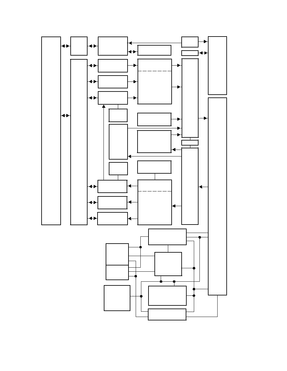
Figure 31 shows a simplified block diagram of the TSB43AB22A device.
32
Received Data
Decoder/Retimer
Arbitration
and Control
State Machine
Logic
Bias Voltage
and
Current Generator
Transmit Data
Encoder
Cable Port 0
Crystal
Oscillator,
PLL System,
and Clock
Generator
Cable Port 1
Internal
Registers
Isochronous
Transmit
Contexts
Asynchronous
Transmit
Contexts
Physical DMA
and Response
PCI
Target
SM
PHY
Register
Access
and
Status
Monitor
Central
Arbiter
and
PCI
Initiator
SM
Cycle Start
Generator and
Cycle Monitor
Synthesized
Bus Reset
Receive
FIFO
Link
Transmit
Link
Receive
PCI
Host
Bus
Interface
Resp
Time-out
Request
Filters
General
Request Receive
Asynchronous
Response
Receive
Isochronous
Receive
Contexts
OHCI PCI Power
Mgmt and CLKRUN
Transmit
FIFO
Receive
Acknowledge
Serial
ROM
GPIOs
CRC
Misc
Interface
PHY/
Link
Interface
Figure 31. TSB43AB22A Block Diagram

33
3.1
PCI Configuration Registers
The TSB43AB22A device is a single-function PCI device. The configuration header is compliant with the PCI Local
Bus Specification as a standard header. Table 32 illustrates the PCI configuration header that includes both the
predefined portion of the configuration space and the user-definable registers.
Table 32. PCI Configuration Register Map
REGISTER NAME
OFFSET
Device ID
Vendor ID
00h
Status
Command
04h
Class code
Revision ID
08h
BIST
Header type
Latency timer
Cache line size
0Ch
OHCI base address
10h
TI extension base address
14h
CardBus CIS base address
18h
Reserved
1Ch27h
CardBus CIS pointer
28h
Subsystem ID
Subsystem vendor ID
2Ch
Reserved
30h
Reserved
PCI power
management
capabilities pointer
34h
Reserved
38h
Maximum latency
Minimum grant
Interrupt pin
Interrupt line
3Ch
OHCI control
40h
Power management capabilities
Next item pointer
Capability ID
44h
PM data
PMCSR_BSE
Power management control and status
48h
Reserved
4ChEBh
PCI PHY control
ECh
Miscellaneous configuration
F0h
Link enhancement control
F4h
Subsystem device ID alias
Subsystem vendor ID alias
F8h
GPIO3
GPIO2
Reserved
FCh
3.2
Vendor ID Register
The vendor ID register contains a value allocated by the PCI SIG and identifies the manufacturer of the PCI device.
The vendor ID assigned to Texas Instruments is 104Ch.
Bit
15
14
13
12
11
10
9
8
7
6
5
4
3
2
1
0
Name
Vendor ID
Type
R
R
R
R
R
R
R
R
R
R
R
R
R
R
R
R
Default
0
0
0
1
0
0
0
0
0
1
0
0
1
1
0
0
Register:
Vendor ID
Offset:
00h
Type:
Read-only
Default:
104Ch

34
3.3
Device ID Register
The device ID register contains a value assigned to the TSB43AB22A device by Texas Instruments. The device
identification for the TSB43AB22A device is 8023h.
Bit
15
14
13
12
11
10
9
8
7
6
5
4
3
2
1
0
Name
Device ID
Type
R
R
R
R
R
R
R
R
R
R
R
R
R
R
R
R
Default
1
0
0
0
0
0
0
0
0
0
1
0
0
0
1
1
Register:
Device ID
Offset:
02h
Type:
Read-only
Default:
8023h
3.4
Command Register
The command register provides control over the TSB43AB22A interface to the PCI bus. All bit functions adhere to
the definitions in the PCI Local Bus Specification, as seen in the following bit descriptions. See Table 33 for a
complete description of the register contents.
Bit
15
14
13
12
11
10
9
8
7
6
5
4
3
2
1
0
Name
Command
Type
R
R
R
R
R
R
R
R/W
R
R/W
R
R/W
R
R/W
R/W
R
Default
0
0
0
0
0
0
0
0
0
0
0
0
0
0
0
0
Register:
Command
Offset:
04h
Type:
Read/Write, Read-only
Default:
0000h
Table 33. Command Register Description
BIT
FIELD NAME
TYPE
DESCRIPTION
1510
RSVD
R
Reserved. Bits 1510 return 0s when read.
9
FBB_ENB
R
Fast back-to-back enable. The TSB43AB22A device does not generate fast back-to-back
transactions; therefore, bit 9 returns 0 when read.
8
SERR_ENB
R/W
PCI_SERR enable. When bit 8 is set to 1, the TSB43AB22A PCI_SERR driver is enabled. PCI_SERR
can be asserted after detecting an address parity error on the PCI bus.
7
STEP_ENB
R
Address/data stepping control. The TSB43AB22A device does not support address/data stepping;
therefore, bit 7 is hardwired to 0.
6
PERR_ENB
R/W
Parity error enable. When bit 6 is set to 1, the TSB43AB22A device is enabled to drive PCI_PERR
response to parity errors through the PCI_PERR signal.
5
VGA_ENB
R
VGA palette snoop enable. The TSB43AB22A device does not feature VGA palette snooping;
therefore, bit 5 returns 0 when read.
4
MWI_ENB
R/W
Memory write and invalidate enable. When bit 4 is set to 1, the TSB43AB22A device is enabled to
generate MWI PCI bus commands. If this bit is cleared, the TSB43AB22A device generates memory
write commands instead.
3
SPECIAL
R
Special cycle enable. The TSB43AB22A function does not respond to special cycle transactions;
therefore, bit 3 returns 0 when read.
2
MASTER_ENB
R/W
Bus master enable. When bit 2 is set to 1, the TSB43AB22A device is enabled to initiate cycles on the
PCI bus.
1
MEMORY_ENB
R/W
Memory response enable. Setting bit 1 to 1 enables the TSB43AB22A device to respond to memory
cycles on the PCI bus. This bit must be set to access OHCI registers.
0
IO_ENB
R
I/O space enable. The TSB43AB22A device does not implement any I/O-mapped functionality;
therefore, bit 0 returns 0 when read.

35
3.5
Status Register
The status register provides status over the TSB43AB22A interface to the PCI bus. All bit functions adhere to the
definitions in the PCI Local Bus Specification, as seen in the following bit descriptions. See Table 34 for a complete
description of the register contents.
Bit
15
14
13
12
11
10
9
8
7
6
5
4
3
2
1
0
Name
Status
Type
RCU
RCU
RCU
RCU
RCU
R
R
RCU
R
R
R
R
R
R
R
R
Default
0
0
0
0
0
0
1
0
0
0
0
1
0
0
0
0
Register:
Status
Offset:
06h
Type:
Read/Clear/Update, Read-only
Default:
0210h
Table 34. Status Register Description
BIT
FIELD NAME
TYPE
DESCRIPTION
15
PAR_ERR
RCU
Detected parity error. Bit 15 is set to 1 when either an address parity or data parity error is detected.
14
SYS_ERR
RCU
Signaled system error. Bit 14 is set to 1 when PCI_SERR is enabled and the TSB43AB22A device has
signaled a system error to the host.
13
MABORT
RCU
Received master abort. Bit 13 is set to 1 when a cycle initiated by the TSB43AB22A device on the PCI
bus has been terminated by a master abort.
12
TABORT_REC
RCU
Received target abort. Bit 12 is set to 1 when a cycle initiated by the TSB43AB22A device on the PCI
bus was terminated by a target abort.
11
TABORT_SIG
RCU
Signaled target abort. Bit 11 is set to 1 by the TSB43AB22A device when it terminates a transaction
on the PCI bus with a target abort.
109
PCI_SPEED
R
DEVSEL timing. Bits 10 and 9 encode the timing of PCI_DEVSEL and are hardwired to 01b, indicating
that the TSB43AB22A device asserts this signal at a medium speed on nonconfiguration cycle
accesses.
8
DATAPAR
RCU
Data parity error detected. Bit 8 is set to 1 when the following conditions have been met:
a. PCI_PERR was asserted by any PCI device including the TSB43AB22A device.
b. The TSB43AB22A device was the bus master during the data parity error.
c. Bit 6 (PERR_EN) in the command register at offset 04h in the PCI configuration space
(see Section 3.4, Command Register) is set to 1.
7
FBB_CAP
R
Fast back-to-back capable. The TSB43AB22A device cannot accept fast back-to-back transactions;
therefore, bit 7 is hardwired to 0.
6
UDF
R
User-definable features (UDF) supported. The TSB43AB22A device does not support the UDF;
therefore, bit 6 is hardwired to 0.
5
66MHZ
R
66-MHz capable. The TSB43AB22A device operates at a maximum PCI_CLK frequency of 33 MHz;
therefore, bit 5 is hardwired to 0.
4
CAPLIST
R
Capabilities list. Bit 4 returns 1 when read, indicating that capabilities additional to standard PCI are
implemented. The linked list of PCI power-management capabilities is implemented in this function.
30
RSVD
R
Reserved. Bits 30 return 0s when read.

36
3.6
Class Code and Revision ID Register
The class code and revision ID register categorizes the TSB43AB22A device as a serial bus controller (0Ch),
controlling an IEEE 1394 bus (00h), with an OHCI programming model (10h). Furthermore, the TI chip revision is
indicated in the least significant byte. See Table 35 for a complete description of the register contents.
Bit
31
30
29
28
27
26
25
24
23
22
21
20
19
18
17
16
Name
Class code and revision ID
Type
R
R
R
R
R
R
R
R
R
R
R
R
R
R
R
R
Default
0
0
0
0
1
1
0
0
0
0
0
0
0
0
0
0
Bit
15
14
13
12
11
10
9
8
7
6
5
4
3
2
1
0
Name
Class code and revision ID
Type
R
R
R
R
R
R
R
R
R
R
R
R
R
R
R
R
Default
0
0
0
1
0
0
0
0
0
0
0
0
0
0
0
0
Register:
Class code and revision ID
Offset:
08h
Type:
Read-only
Default:
0C00 1000h
Table 35. Class Code and Revision ID Register Description
BIT
FIELD NAME
TYPE
DESCRIPTION
3124
BASECLASS
R
Base class. This field returns 0Ch when read, which broadly classifies the function as a serial bus
controller.
2316
SUBCLASS
R
Subclass. This field returns 00h when read, which specifically classifies the function as controlling an
IEEE 1394 serial bus.
158
PGMIF
R
Programming interface. This field returns 10h when read, which indicates that the programming model
is compliant with the 1394 Open Host Controller Interface Specification.
70
CHIPREV
R
Silicon revision. This field returns 00h when read, which indicates the silicon revision of the
TSB43AB22A device.
3.7
Latency Timer and Class Cache Line Size Register
The latency timer and class cache line size register is programmed by host BIOS to indicate system cache line size
and the latency timer associated with the TSB43AB22A device. See Table 36 for a complete description of the
register contents.
Bit
15
14
13
12
11
10
9
8
7
6
5
4
3
2
1
0
Name
Latency timer and class cache line size
Type
R/W
R/W
R/W
R/W
R/W
R/W
R/W
R/W
R/W
R/W
R/W
R/W
R/W
R/W
R/W
R/W
Default
0
0
0
0
0
0
0
0
0
0
0
0
0
0
0
0
Register:
Latency timer and class cache line size
Offset:
0Ch
Type:
Read/Write
Default:
0000h
Table 36. Latency Timer and Class Cache Line Size Register Description
BIT
FIELD NAME
TYPE
DESCRIPTION
158
LATENCY_TIMER
R/W
PCI latency timer. The value in this register specifies the latency timer for the TSB43AB22A device,
in units of PCI clock cycles. When the TSB43AB22A device is a PCI bus initiator and asserts
PCI_FRAME, the latency timer begins counting from zero. If the latency timer expires before the
TSB43AB22A transaction has terminated, the TSB43AB22A device terminates the transaction when
its PCI_GNT is deasserted.
70
CACHELINE_SZ
R/W
Cache line size. This value is used by the TSB43AB22A device during memory write and invalidate,
memory-read line, and memory-read multiple transactions.

37
3.8
Header Type and BIST Register
The header type and built-in self-test (BIST) register indicates the TSB43AB22A PCI header type and no built-in
self-test. See Table 37 for a complete description of the register contents.
Bit
15
14
13
12
11
10
9
8
7
6
5
4
3
2
1
0
Name
Header type and BIST
Type
R
R
R
R
R
R
R
R
R
R
R
R
R
R
R
R
Default
0
0
0
0
0
0
0
0
0
0
0
0
0
0
0
0
Register:
Header type and BIST
Offset:
0Eh
Type:
Read-only
Default:
0000h
Table 37. Header Type and BIST Register Description
BIT
FIELD NAME
TYPE
DESCRIPTION
158
BIST
R
Built-in self-test. The TSB43AB22A device does not include a BIST; therefore, this field returns 00h
when read.
70
HEADER_TYPE
R
PCI header type. The TSB43AB22A device includes the standard PCI header, which is communicated
by returning 00h when this field is read.
3.9
OHCI Base Address Register
The OHCI base address register is programmed with a base address referencing the memory-mapped OHCI control.
When BIOS writes all 1s to this register, the value read back is FFFF F800h, indicating that at least 2K bytes of
memory address space are required for the OHCI registers. See Table 38 for a complete description of the register
contents.
Bit
31
30
29
28
27
26
25
24
23
22
21
20
19
18
17
16
Name
OHCI base address
Type
R/W
R/W
R/W
R/W
R/W
R/W
R/W
R/W
R/W
R/W
R/W
R/W
R/W
R/W
R/W
R/W
Default
0
0
0
0
0
0
0
0
0
0
0
0
0
0
0
0
Bit
15
14
13
12
11
10
9
8
7
6
5
4
3
2
1
0
Name
OHCI base address
Type
R/W
R/W
R/W
R/W
R/W
R
R
R
R
R
R
R
R
R
R
R
Default
0
0
0
0
0
0
0
0
0
0
0
0
0
0
0
0
Register:
OHCI base address
Offset:
10h
Type:
Read/Write, Read-only
Default:
0000 0000h
Table 38. OHCI Base Address Register Description
BIT
FIELD NAME
TYPE
DESCRIPTION
3111
OHCIREG_PTR
R/W
OHCI register pointer. This field specifies the upper 21 bits of the 32-bit OHCI base address register.
104
OHCI_SZ
R
OHCI register size. This field returns 0s when read, indicating that the OHCI registers require a
2K-byte region of memory.
3
OHCI_PF
R
OHCI register prefetch. Bit 3 returns 0 when read, indicating that the OHCI registers are
nonprefetchable.
21
OHCI_MEMTYPE
R
OHCI memory type. This field returns 0s when read, indicating that the OHCI base address register
is 32 bits wide and mapping can be done anywhere in the 32-bit memory space.
0
OHCI_MEM
R
OHCI memory indicator. Bit 0 returns 0 when read, indicating that the OHCI registers are mapped
into system memory space.

38
3.10 TI Extension Base Address Register
The TI extension base address register is programmed with a base address referencing the memory-mapped TI
extension registers. When BIOS writes all 1s to this register, the value read back is FFFF C000h, indicating that at
least 16K bytes of memory address space are required for the TI registers. See Table 39 for a complete description
of the register contents.
Bit
31
30
29
28
27
26
25
24
23
22
21
20
19
18
17
16
Name
TI extension base address
Type
R/W
R/W
R/W
R/W
R/W
R/W
R/W
R/W
R/W
R/W
R/W
R/W
R/W
R/W
R/W
R/W
Default
0
0
0
0
0
0
0
0
0
0
0
0
0
0
0
0
Bit
15
14
13
12
11
10
9
8
7
6
5
4
3
2
1
0
Name
TI extension base address
Type
R/W
R/W
R
R
R
R
R
R
R
R
R
R
R
R
R
R
Default
0
0
0
0
0
0
0
0
0
0
0
0
0
0
0
0
Register:
TI extension base address
Offset:
14h
Type:
Read/Write, Read-only
Default:
0000 0000h
Table 39. TI Base Address Register Description
BIT
FIELD NAME
TYPE
DESCRIPTION
3114
TIREG_PTR
R/W
TI register pointer. This field specifies the upper 18 bits of the 32-bit TI base address register.
134
TI_SZ
R
TI register size. This field returns 0s when read, indicating that the TI registers require a 16K-byte
region of memory.
3
TI_PF
R
TI register prefetch. Bit 3 returns 0 when read, indicating that the TI registers are nonprefetchable.
21
TI_MEMTYPE
R
TI memory type. This field returns 0s when read, indicating that the TI base address register is 32 bits
wide and mapping can be done anywhere in the 32-bit memory space.
0
TI_MEM
R
TI memory indicator. Bit 0 returns 0 when read, indicating that the TI registers are mapped into system
memory space.

39
3.11 CardBus CIS Base Address Register
If CARDBUS is sampled high on a G_RST, this 32-bit register returns 0s when read. If CARDBUS is sampled low,
this register is programmed with a base address referencing the memory-mapped card information structure (CIS).
This register must be programmed with a nonzero value before the CIS can be accessed. See Table 310 for a
complete description of the register contents.
Bit
31
30
29
28
27
26
25
24
23
22
21
20
19
18
17
16
Name
CardBus CIS base address
Type
R/W
R/W
R/W
R/W
R/W
R/W
R/W
R/W
R/W
R/W
R/W
R/W
R/W
R/W
R/W
R/W
Default
0
0
0
0
0
0
0
0
0
0
0
0
0
0
0
0
Bit
15
14
13
12
11
10
9
8
7
6
5
4
3
2
1
0
Name
CardBus CIS base address
Type
R/W
R/W
R/W
R/W
R/W
R
R
R
R
R
R
R
R
R
R
R
Default
0
0
0
0
0
0
0
0
0
0
0
0
0
0
0
0
Register:
CardBus CIS base address
Offset:
18h
Type:
Read/Write, Read-only
Default:
0000 0000h
Table 310. CardBus CIS Base Address Register Description
BIT
FIELD NAME
TYPE
DESCRIPTION
3111
CIS_BASE
R/W
CIS base address. This field specifies the upper 21 bits of the 32-bit CIS base address. If CARDBUS
is sampled high on a G_RST, this field is read-only, returning 0s when read.
104
CIS_SZ
R
CIS address space size. This field returns 0s when read, indicating that the CIS space requires a
2K-byte region of memory.
3
CIS_PF
R
CIS prefetch. Bit 3 returns 0 when read, indicating that the CIS is nonprefetchable. Furthermore, the
CIS is a byte-accessible address space, and either a doubleword or 16-bit word access yields
indeterminate results.
21
CIS_MEMTYPE
R
CIS memory type. This field returns 0s when read, indicating that the CardBus CIS base address
register is 32 bits wide and mapping can be done anywhere in the 32-bit memory space.
0
CIS_MEM
R
CIS memory indicator. Bit 0 returns 0 when read, indicating that the CIS is mapped into system
memory space.

310
3.12 CardBus CIS Pointer Register
CARDBUS to the TSB43AB22A device is sampled at G_RST to determine the TSB43AB22A application. If
CARDBUS is sampled high, this register is read-only returning 0s when read. If CARDBUS is sampled low, this
register contains the pointer to the CardBus card information structure (CIS). See Table 311 for a complete
description of the register contents.
Bit
31
30
29
28
27
26
25
24
23
22
21
20
19
18
17
16
Name
CardBus CIS pointer
Type
R
R
R
R
R
R
R
R
R
R
R
R
R
R
R
R
Default
0
0
0
0
0
0
0
0
0
0
0
0
0
0
0
0
Bit
15
14
13
12
11
10
9
8
7
6
5
4
3
2
1
0
Name
CardBus CIS pointer
Type
R
R
R
R
R
R
R
R
R
R
R
R
R
R
R
R
Default
0
0
0
0
0
0
0
0
0
0
0
0
0
0
0
0
Register:
CardBus CIS pointer
Offset:
28h
Type:
Read-only
Default:
0000 0000h
Table 311. CardBus CIS Pointer Register Description
BIT
FIELD NAME
TYPE
DESCRIPTION
3128
ROM_IMAGE
R
Since the CIS is not implemented as a ROM image, this field returns 0s when read.
273
CIS_OFFSET
R
This field indicates the offset into the CIS address space where the CIS begins, and bits 73 are
loaded from the serial EEPROM field CIS_Offset (73). This implementation allows the
TSB43AB22A device to produce serial EEPROM addresses equal to the lower PCI address byte to
acquire data from the serial EEPROM.
20
CIS_INDICATOR
R
This field indicates the address space where the CIS resides and returns 011b if CARDBUS is
sampled low at G_RST. 011b indicates that CardBus CIS base address register at offset 18h in the
PCI configuration header contains the CIS base address. If CARDBUS is sampled high at G_RST,
this field contains 000b.

311
3.13 Subsystem Identification Register
The subsystem identification register is used for system and option card identification purposes. This register can
be initialized from the serial EEPROM or programmed via the subsystem access register at offset F8h in the PCI
configuration space (see Section 3.25, Subsystem Access Register). See Table 312 for a complete description of
the register contents.
Bit
31
30
29
28
27
26
25
24
23
22
21
20
19
18
17
16
Name
Subsystem identification
Type
RU
RU
RU
RU
RU
RU
RU
RU
RU
RU
RU
RU
RU
RU
RU
RU
Default
0
0
0
0
0
0
0
0
0
0
0
0
0
0
0
0
Bit
15
14
13
12
11
10
9
8
7
6
5
4
3
2
1
0
Name
Subsystem identification
Type
RU
RU
RU
RU
RU
RU
RU
RU
RU
RU
RU
RU
RU
RU
RU
RU
Default
0
0
0
0
0
0
0
0
0
0
0
0
0
0
0
0
Register:
Subsystem identification
Offset:
2Ch
Type:
Read/Update
Default:
0000 0000h
Table 312. Subsystem Identification Register Description
BIT
FIELD NAME
TYPE
DESCRIPTION
3116
OHCI_SSID
RU
Subsystem device ID. This field indicates the subsystem device ID.
150
OHCI_SSVID
RU
Subsystem vendor ID. This field indicates the subsystem vendor ID.
3.14 Power Management Capabilities Pointer Register
The power management capabilities pointer register provides a pointer into the PCI configuration header where the
power-management register block resides. The TSB43AB22A configuration header doublewords at offsets 44h and
48h provide the power-management registers. This register is read-only and returns 44h when read.
Bit
7
6
5
4
3
2
1
0
Name
Power management capabilities pointer
Type
R
R
R
R
R
R
R
R
Default
0
1
0
0
0
1
0
0
Register:
Power management capabilities pointer
Offset:
34h
Type:
Read-only
Default:
44h

312
3.15 Interrupt Line and Pin Register
The interrupt line and pin register communicates interrupt line routing information. See Table 313 for a complete
description of the register contents.
Bit
15
14
13
12
11
10
9
8
7
6
5
4
3
2
1
0
Name
Interrupt line and pin
Type
R
R
R
R
R
R
R
R
R/W
R/W
R/W
R/W
R/W
R/W
R/W
R/W
Default
0
0
0
0
0
0
0
1
0
0
0
0
0
0
0
0
Register:
Interrupt line and pin
Offset:
3Ch
Type:
Read/Write
Default:
0100h
Table 313. Interrupt Line and Pin Registers Description
BIT
FIELD NAME
TYPE
DESCRIPTION
158
INTR_PIN
R
Interrupt pin. This field returns 01h when read, indicating that the TSB43AB22A PCI function signals
interrupts on the PCI_INTA terminal.
70
INTR_LINE
R/W
Interrupt line. This field is programmed by the system and indicates to software which interrupt line the
TSB43AB22A PCI_INTA is connected to.
3.16 MIN_GNT and MAX_LAT Register
The MIN_GNT and MAX_LAT register communicates to the system the desired setting of bits 158 in the latency timer
and class cache line size register at offset 0Ch in the PCI configuration space (see Section 3.7, Latency Timer and
Class Cache Line Size Register). If a serial EEPROM is detected, the contents of this register are loaded through
the serial EEPROM interface after a G_RST. If no serial EEPROM is detected, this register returns a default value
that corresponds to the MAX_LAT = 4, MIN_GNT = 2. See Table 314 for a complete description of the register
contents.
Bit
15
14
13
12
11
10
9
8
7
6
5
4
3
2
1
0
Name
MIN_GNT and MAX_LAT
Type
RU
RU
RU
RU
RU
RU
RU
RU
RU
RU
RU
RU
RU
RU
RU
RU
Default
0
0
0
0
0
1
0
0
0
0
0
0
0
0
1
0
Register:
MIN_GNT and MAX_LAT
Offset:
3Eh
Type:
Read/Update
Default:
0402h
Table 314. MIN_GNT and MAX_LAT Register Description
BIT
FIELD NAME
TYPE
DESCRIPTION
158
MAX_LAT
RU
Maximum latency. The contents of this field may be used by host BIOS to assign an arbitration priority level
to the TSB43AB22A device. The default for this register indicates that the TSB43AB22A device may need
to access the PCI bus as often as every 0.25
µ
s; thus, an extremely high priority level is requested. The
contents of this field may also be loaded through the serial EEPROM.
70
MIN_GNT
RU
Minimum grant. The contents of this field may be used by host BIOS to assign a latency timer register value
to the TSB43AB22A device. The default for this register indicates that the TSB43AB22A device may need
to sustain burst transfers for nearly 64
µ
s and thus request a large value be programmed in bits 158 of
the TSB43AB22A latency timer and class cache line size register at offset 0Ch in the PCI configuration
space (see Section 3.7, Latency Timer and Class Cache Line Size Register).

313
3.17 OHCI Control Register
The PCI OHCI control register is defined by the 1394 Open Host Controller Interface Specification and provides a
bit for big endian PCI support. See Table 315 for a complete description of the register contents.
Bit
31
30
29
28
27
26
25
24
23
22
21
20
19
18
17
16
Name
OHCI control
Type
R
R
R
R
R
R
R
R
R
R
R
R
R
R
R
R
Default
0
0
0
0
0
0
0
0
0
0
0
0
0
0
0
0
Bit
15
14
13
12
11
10
9
8
7
6
5
4
3
2
1
0
Name
OHCI control
Type
R
R
R
R
R
R
R
R
R
R
R
R
R
R
R
R/W
Default
0
0
0
0
0
0
0
0
0
0
0
0
0
0
0
0
Register:
OHCI control
Offset:
40h
Type:
Read/Write, read-only
Default:
0000 0000h
Table 315. OHCI Control Register Description
BIT
FIELD NAME
TYPE
DESCRIPTION
311
RSVD
R
Reserved. Bits 311 return 0s when read.
0
GLOBAL_SWAP
R/W
When bit 0 is set to 1, all quadlets read from and written to the PCI interface are byte-swapped (big
endian).
3.18 Capability ID and Next Item Pointer Registers
The capability ID and next item pointer register identifies the linked-list capability item and provides a pointer to the
next capability item. See Table 316 for a complete description of the register contents.
Bit
15
14
13
12
11
10
9
8
7
6
5
4
3
2
1
0
Name
Capability ID and next item pointer
Type
R
R
R
R
R
R
R
R
R
R
R
R
R
R
R
R
Default
0
0
0
0
0
0
0
0
0
0
0
0
0
0
0
1
Register:
Capability ID and next item pointer
Offset:
44h
Type:
Read-only
Default:
0001h
Table 316. Capability ID and Next Item Pointer Registers Description
BIT
FIELD NAME
TYPE
DESCRIPTION
158
NEXT_ITEM
R
Next item pointer. The TSB43AB22A device supports only one additional capability that is
communicated to the system through the extended capabilities list; therefore, this field returns 00h
when read.
70
CAPABILITY_ID
R
Capability identification. This field returns 01h when read, which is the unique ID assigned by the PCI
SIG for PCI power-management capability.

314
3.19 Power Management Capabilities Register
The power management capabilities register indicates the capabilities of the TSB43AB22A device related to PCI
power management. See Table 317 for a complete description of the register contents.
Bit
15
14
13
12
11
10
9
8
7
6
5
4
3
2
1
0
Name
Power management capabilities
Type
RU
R
R
R
R
R
R
R
R
R
R
R
R
R
R
R
Default
0
1
1
1
1
1
1
0
0
0
0
0
0
0
1
0
Register:
Power management capabilities
Offset:
46h
Type:
Read/Update, Read-only
Default:
7E02h
Table 317. Power Management Capabilities Register Description
BIT
FIELD NAME
TYPE
DESCRIPTION
15
PME_D3COLD
RU
PCI_PME support from D3cold. This bit can be set to 1 or cleared to 0 via bit 15 (PME_D3COLD) in
the miscellaneous configuration register at offset F0h in the PCI configuration space (see Section 3.23,
Miscellaneous Configuration Register). The miscellaneous configuration register is loaded from ROM.
When this bit is set to 1, it indicates that the TSB43AB22A device is capable of generating a PCI_PME
wake event from D3cold. This bit state is dependent upon the TSB43AB22A VAUX implementation and
may be configured by using bit 15 (PME_D3COLD) in the miscellaneous configuration register (see
Section 3.23).
1411
PME_SUPPORT
R
PCI_PME support. This 4-bit field indicates the power states from which the TSB43AB22A device may
assert PCI_PME. This field returns a value of 1111b by default, indicating that PCI_PME may be
asserted from the D3hot, D2, D1, and D0 power states.
10
D2_SUPPORT
R
D2 support. Bit 10 is hardwired to 1, indicating that the TSB43AB22A device supports the D2 power
state.
9
D1_SUPPORT
R
D1 support. Bit 9 is hardwired to 1, indicating that the TSB43AB22A device supports the D1 power
state.
86
AUX_CURRENT
R
Auxiliary current. This 3-bit field reports the 3.3-VAUX auxiliary current requirements. When bit 15
(PME_D3COLD) is cleared, this field returns 000b; otherwise, it returns 001b.
000b = Self-powered
001b = 55 mA (3.3-VAUX maximum current required)
5
DSI
R
Device-specific initialization. This bit returns 0 when read, indicating that the TSB43AB22A device
does not require special initialization beyond the standard PCI configuration header before a generic
class driver is able to use it.
4
RSVD
R
Reserved. Bit 4 returns 0 when read.
3
PME_CLK
R
PCI_PME clock. This bit returns 0 when read, indicating that no host bus clock is required for the
TSB43AB22A device to generate PCI_PME.
20
PM_VERSION
R
Power-management version. This field returns 010b when read, indicating that the TSB43AB22A
device is compatible with the registers described in the PCI Bus Power Management Interface
Specification (Revision 1.1).

315
3.20 Power Management Control and Status Register
The power management control and status register implements the control and status of the PCI power management
function. This register is not affected by the internally generated reset caused by the transition from the D3
hot
to D0
state. See Table 318 for a complete description of the register contents.
Bit
15
14
13
12
11
10
9
8
7
6
5
4
3
2
1
0
Name
Power management control and status
Type
RWC
R
R
R
R
R
R
R/W
R
R
R
R
R
R
R/W
R/W
Default
0
0
0
0
0
0
0
0
0
0
0
0
0
0
0
0
Register:
Power management control and status
Offset:
48h
Type:
Read/Clear, Read/Write, Read-only
Default:
0000h
Table 318. Power Management Control and Status Register Description
BIT
FIELD NAME
TYPE
DESCRIPTION
15
PME_STS
RWC
Bit 15 is set to 1 when the TSB43AB22A device normally asserts the PCI_PME signal independent
of the state of bit 8 (PME_ENB). This bit is cleared by a writeback of 1, which also clears the PCI_PME
signal driven by the TSB43AB22A device. Writing a 0 to this bit has no effect.
1413
DATA_SCALE
R
This field returns 0s, because the data register is not implemented.
129
DATA_SELECT
R
This field returns 0s, because the data register is not implemented.
8
PME_ENB
R/W
When bit 8 is set to 1, PME assertion is enabled. When bit 8 is cleared, PME assertion is disabled. This
bit defaults to 0 if the function does not support PME generation from D3cold. If the function supports
PME from D3cold, this bit is sticky and must be explicitly cleared by the operating system each time
it is initially loaded.
72
RSVD
R
Reserved. Bits 72 return 0s when read.
10
PWR_STATE
R/W
Power state. This 2-bit field sets the TSB43AB22A device power state and is encoded as follows:
00 = Current power state is D0.
01 = Current power state is D1.
10 = Current power state is D2.
11 = Current power state is D3.
3.21 Power Management Extension Registers
The power management extension register provides extended power-management features not applicable to the
TSB43AB22A device; thus, it is read-only and returns 0 when read. See Table 319 for a complete description of the
register contents.
Bit
15
14
13
12
11
10
9
8
7
6
5
4
3
2
1
0
Name
Power management extension
Type
R
R
R
R
R
R
R
R
R
R
R
R
R
R
R
R
Default
0
0
0
0
0
0
0
0
0
0
0
0
0
0
0
0
Register:
Power management extension
Offset:
4Ah
Type:
Read-only
Default:
0000h
Table 319. Power Management Extension Registers Description
BIT
FIELD NAME
TYPE
DESCRIPTION
150
RSVD
R
Reserved. Bits 150 return 0s when read.

316
3.22 PCI PHY Control Register
The PCI PHY control register provides a method for enabling the PHY CNA output. See Table 320 for a complete
description of the register contents.
Bit
31
30
29
28
27
26
25
24
23
22
21
20
19
18
17
16
Name
PCI PHY control
Type
R
R
R
R
R
R
R
R
R
R
R
R
R
R
R
R
Default
0
0
0
0
0
0
0
0
0
0
0
0
0
0
0
0
Bit
15
14
13
12
11
10
9
8
7
6
5
4
3
2
1
0
Name
PCI PHY control
Type
R
R
R
R
R
R
R
R
R/W
R
R
R
R/W
R
R
R
Default
0
0
0
0
0
0
0
0
0
0
0
0
1
0
0
0
Register:
PCI PHY control
Offset:
ECh
Type:
Read/Write, read-only
Default:
0000 0008h
Table 320. PCI PHY Control Register
BIT
FIELD NAME
TYPE
DESCRIPTION
318
RSVD
R
Reserved. Bits 318 return 0s when read.
7
CNAOUT
R/W
When bit 7 is set to 1, the PHY CNA output is routed to terminal 96. When implementing a serial
EEPROM, this bit can be set by programming bit 7 of offset 16h in the EEPROM to 1.
64
RSVD
R
Reserved. Bits 64 return 0s when read. These bits are affected when implementing a serial
EEPROM; thus, bits 64 at EEPROM byte offset 16h must be programmed to 0.
3
RSVD
R
Reserved. Bit 3 defaults to 1 to indicate compliance with IEEE Std 1394a-2000. If a serial
EEPROM is implemented, bit 3 at EEPROM byte offset 16h must be set to 1. See Table 62,
Serial EEPROM Map.
20
RSVD
R
Reserved. Bits 20 return 0s when read. These bits are affected when implementing a serial
EEPROM; thus, bits 20 at EEPROM byte offset 16h must be programmed to 0.

317
3.23 Miscellaneous Configuration Register
The miscellaneous configuration register provides miscellaneous PCI-related configuration. See Table 321 for a
complete description of the register contents.
Bit
31
30
29
28
27
26
25
24
23
22
21
20
19
18
17
16
Name
Miscellaneous configuration
Type
R
R
R
R
R
R
R
R
R
R
R
R
R
R
R
R
Default
0
0
0
0
0
0
0
0
0
0
0
0
0
0
0
0
Bit
15
14
13
12
11
10
9
8
7
6
5
4
3
2
1
0
Name
Miscellaneous configuration
Type
R/W
R
R/W
R
R
R/W
R
R
R
R
R
R/W
R/W
R/W
R/W
R/W
Default
0
0
0
0
0
0
0
0
0
0
0
0
0
0
0
0
Register:
Miscellaneous configuration
Offset:
F0h
Type:
Read/Write, read-only
Default:
0000 0000h
Table 321. Miscellaneous Configuration Register
BIT
FIELD NAME
TYPE
DESCRIPTION
3116
RSVD
R
Reserved. Bits 3116 return 0s when read.
15
PME_D3COLD
R/W
PCI_PME support from D3cold. This bit programs bit 15 (PME_D3COLD) in the power
management capabilities register at offset 46h in the PCI configuration space (see Section 3.19,
Power Management Capabilities Register).
145
RSVD
R
Reserved. Bits 145 return 0s when read.
4
DIS_TGT_ABT
R/W
Bit 4 defaults to 0, which provides OHCI-Lynx
compatible target abort signaling. When this bit
is set to 1, it enables the no-target-abort mode, in which the TSB43AB22A device returns
indeterminate data instead of signaling target abort.
The TSB43AB22A LLC is divided into the PCI_CLK and SCLK domains. If software tries to access
registers in the link that are not active because the SCLK is disabled, a target abort is issued by
the link. On some systems, this can cause a problem resulting in a fatal system error. Enabling
this bit allows the link to respond to these types of requests by returning FFh.
It is recommended that this bit be set to 1.
3
GP2IIC
R/W
When bit 3 is set to 1, the GPIO3 and GPIO2 signals are internally routed to the SCL and SDA,
respectively. The GPIO3 and GPIO2 terminals are also placed in the high-impedance state.
2
DISABLE_SCLKGATE
R/W
When bit 2 is set to 1, the internal SCLK runs identically with the chip input. This is a test feature
only and must be cleared to 0 (all applications).
1
DISABLE_PCIGATE
R/W
When bit 1 is set to 1, the internal PCI clock runs identically with the chip input. This is a test feature
only and must be cleared to 0 (all applications).
0
KEEP_PCLK
R/W
When bit 0 is set to 1, the PCI clock is always kept running through the PCI_CLKRUN protocol.
When this bit is cleared, the PCI clock can be stopped using PCI_CLKRUN.

318
3.24 Link Enhancement Control Register
The link enhancement control register implements TI proprietary bits that are initialized by software or by a serial
EEPROM, if present. After these bits are set to 1, their functionality is enabled only if bit 22 (aPhyEnhanceEnable)
in the host controller control register at OHCI offset 50h/54h (see Section 4.16, Host Controller Control Register) is
set to 1. See Table 322 for a complete description of the register contents.
Bit
31
30
29
28
27
26
25
24
23
22
21
20
19
18
17
16
Name
Link enhancement control
Type
R
R
R
R
R
R
R
R
R
R
R
R
R
R
R
R
Default
0
0
0
0
0
0
0
0
0
0
0
0
0
0
0
0
Bit
15
14
13
12
11
10
9
8
7
6
5
4
3
2
1
0
Name
Link enhancement control
Type
R/W
R
R/W
R/W
R
R/W
R
R/W
R/W
R
R
R
R
R
R/W
R
Default
0
0
0
1
0
0
0
0
0
0
0
0
0
0
0
0
Register:
Link enhancement control
Offset:
F4h
Type:
Read/Write, read-only
Default:
0000 1000h
Table 322. Link Enhancement Control Register Description
BIT
FIELD NAME
TYPE
DESCRIPTION
3116
RSVD
R
Reserved. Bits 3116 return 0s when read.
15
dis_at_pipeline
R/W
Disable AT pipelining. When bit 15 is set to 1, out-of-order AT pipelining is disabled.
14
RSVD
R
Reserved.
1312
atx_thresh
R/W
This field sets the initial AT threshold value, which is used until the AT FIFO is underrun. When the
TSB43AB22A device retries the packet, it uses a 2K-byte threshold, resulting in a store-and-forward
operation.
00 = Threshold ~ 2K bytes resulting in a store-and-forward operation
01 = Threshold ~ 1.7K bytes (default)
10 = Threshold ~ 1K bytes
11 = Threshold ~ 512 bytes
These bits fine-tune the asynchronous transmit threshold. For most applications the 1.7K-byte
threshold is optimal. Changing this value may increase or decrease the 1394 latency depending on
the average PCI bus latency.
Setting the AT threshold to 1.7K, 1K, or 512 bytes results in data being transmitted at these thresholds
or when an entire packet has been checked into the FIFO. If the packet to be transmitted is larger than
the AT threshold, the remaining data must be received before the AT FIFO is emptied; otherwise, an
underrun condition occurs, resulting in a packet error at the receiving node. As a result, the link then
commences store-and-forward operation. Wait until it has the complete packet in the FIFO before
retransmitting it on the second attempt to ensure delivery.
An AT threshold of 2K results in store-and-forward operation, which means that asynchronous data
will not be transmitted until an end-of-packet token is received. Restated, setting the AT threshold to
2K results in only complete packets being transmitted.
Note that this device will always use store-and-forward when the asynchronous transmit retries
register at OHCI offset 08h (see Section 4.3, Asynchronous Transmit Retries Register) is cleared.
11
RSVD
R
Reserved. Bit 11 returns 0 when read.
10
enab_mpeg_ts
R/W
Enable MPEG CIP timestamp enhancement. When bit 9 is set to 1, the enhancement is enabled for
MPEG CIP transmit streams (FMT = 20h).
9
RSVD
R
Reserved. Bit 9 returns 0 when read.
8
enab_dv_ts
R/W
Enable DV CIP timestamp enhancement. When bit 8 is set to 1, the enhancement is enabled for DV
CIP transmit streams (FMT = 00h).
7
enab_unfair
R/W
Enable asynchronous priority requests. OHCI-Lynx
compatible. Setting bit 7 to 1 enables the link to
respond to requests with priority arbitration. It is recommended that this bit be set to 1.

319
Table 322. Link Enhancement Control Register Description (Continued)
BIT
FIELD NAME
TYPE
DESCRIPTION
6
RSVD
R
This bit is not assigned in the TSB43AB22A follow-on products, because this bit location loaded by
the serial EEPROM from the enhancements field corresponds to bit 23 (programPhyEnable) in the
host controller control register at OHCI offset 50h/54h (see Section 4.16, Host Controller Control
Register).
52
RSVD
R
Reserved. Bits 52 return 0s when read.
1
enab_accel
R/W
Enable acceleration enhancements. OHCI-Lynx
compatible. When bit 1 is set to 1, the PHY layer
is notified that the link supports the IEEE Std 1394a-2000 acceleration enhancements, that is,
ack-accelerated, fly-by concatenation, etc. It is recommended that this bit be set to 1.
0
RSVD
R
Reserved. Bit 0 returns 0 when read.
3.25 Subsystem Access Register
Write access to the subsystem access register updates the subsystem identification registers identically to
OHCI-Lynx
. The system ID value written to this register may also be read back from this register. See Table 323
for a complete description of the register contents.
Bit
31
30
29
28
27
26
25
24
23
22
21
20
19
18
17
16
Name
Subsystem access
Type
R/W
R/W
R/W
R/W
R/W
R/W
R/W
R/W
R/W
R/W
R/W
R/W
R/W
R/W
R/W
R/W
Default
0
0
0
0
0
0
0
0
0
0
0
0
0
0
0
0
Bit
15
14
13
12
11
10
9
8
7
6
5
4
3
2
1
0
Name
Subsystem access
Type
R/W
R/W
R/W
R/W
R/W
R/W
R/W
R/W
R/W
R/W
R/W
R/W
R/W
R/W
R/W
R/W
Default
0
0
0
0
0
0
0
0
0
0
0
0
0
0
0
0
Register:
Subsystem access
Offset:
F8h
Type:
Read/Write
Default:
0000 0000h
Table 323. Subsystem Access Register Description
BIT
FIELD NAME
TYPE
DESCRIPTION
3116
SUBDEV_ID
R/W
Subsystem device ID alias. This field indicates the subsystem device ID.
150
SUBVEN_ID
R/W
Subsystem vendor ID alias. This field indicates the subsystem vendor ID.

320
3.26 GPIO Control Register
The GPIO control register has the control and status bits for the GPIO2 and GPIO3 ports. See Table 324 for a
complete description of the register contents.
Bit
31
30
29
28
27
26
25
24
23
22
21
20
19
18
17
16
Name
GPIO control
Type
R/W
R
R/W
R/W
R
R
R
RWU
R/W
R
R/W
R/W
R
R
R
RWU
Default
0
0
0
0
0
0
0
0
0
0
0
0
0
0
0
0
Bit
15
14
13
12
11
10
9
8
7
6
5
4
3
2
1
0
Name
GPIO control
Type
R
R
R
R
R
R
R
R
R
R
R
R
R
R
R
R
Default
0
0
0
0
0
0
0
0
0
0
0
0
0
0
0
0
Register:
GPIO control
Offset:
FCh
Type:
Read/Write/Update, read/write, read-only
Default:
0000 0000h
Table 324. General-Purpose Input/Output Control Register Description
BIT
FIELD NAME
TYPE
DESCRIPTION
31
INT_3EN
R/W
When bit 31 is set to 1, a TSB43AB22A general-purpose interrupt event occurs on a level change of
the GPIO3 input. This event can generate an interrupt, with mask and event status reported through
the interrupt mask register at OHCI offset 88h/8Ch (see Section 4.22, Interrupt Mask Register) and
interrupt event register at OHCI offset 80h/84h (see Section 4.21, Interrupt Event Register).
30
RSVD
R
Reserved. Bit 30 returns 0 when read.
29
GPIO_INV3
R/W
GPIO3 polarity invert. When bit 29 is set to 1, the polarity of GPIO3 is inverted.
28
GPIO_ENB3
R/W
GPIO3 enable control. When bit 28 is set to 1, the output is enabled. Otherwise, the output is high
impedance.
2725
RSVD
R
Reserved. Bits 2725 return 0s when read.
24
GPIO_DATA3
RWU
GPIO3 data. Reads from bit 24 return the logical value of the input to GPIO3. Writes to this bit update
the value to drive to GPIO3 when output is enabled.
23
INT_2EN
R/W
When bit 23 is set to 1, a TSB43AB22A general-purpose interrupt event occurs on a level change of
the GPIO2 input. This event can generate an interrupt, with mask and event status reported through
the interrupt mask register at OHCI offset 88h/8Ch (see Section 4.22, Interrupt Mask Register) and
interrupt event register at OHCI offset 80h/84h (see Section 4.21, Interrupt Event Register).
22
RSVD
R
Reserved. Bit 22 returns 0 when read.
21
GPIO_INV2
R/W
GPIO2 polarity invert. When bit 21 is set to 1, the polarity of GPIO2 is inverted.
20
GPIO_ENB2
R/W
GPIO2 enable control. When bit 20 is set to 1, the output is enabled. Otherwise, the output is high
impedance.
1917
RSVD
R
Reserved. Bits 1917 return 0s when read.
16
GPIO_DATA2
RWU
GPIO2 data. Reads from bit 16 return the logical value of the input to GPIO2. Writes to this bit update
the value to drive to GPIO2 when the output is enabled.
150
RSVD
R
Reserved. Bits 150 return 0s when read.

41
4 OHCI Registers
The OHCI registers defined by the 1394 Open Host Controller Interface Specification are memory-mapped into a
2K-byte region of memory pointed to by the OHCI base address register at offset 10h in PCI configuration space (see
Section 3.9, OHCI Base Address Register). These registers are the primary interface for controlling the TSB43AB22A
IEEE 1394 link function.
This section provides the register interface and bit descriptions. Several set/clear register pairs in this programming
model are implemented to solve various issues with typical read-modify-write control registers. There are two
addresses for a set/clear register: RegisterSet and RegisterClear. See Table 41 for a register listing. A 1 bit written
to RegisterSet causes the corresponding bit in the set/clear register to be set to 1; a 0 bit leaves the corresponding
bit unaffected. A 1 bit written to RegisterClear causes the corresponding bit in the set/clear register to be cleared;
a 0 bit leaves the corresponding bit in the set/clear register unaffected.
Typically, a read from either RegisterSet or RegisterClear returns the contents of the set or clear register, respectively.
However, sometimes reading the RegisterClear provides a masked version of the set or clear register. The interrupt
event register is an example of this behavior.
Table 41. OHCI Register Map
DMA CONTEXT
REGISTER NAME
ABBREVIATION
OFFSET
--
OHCI version
Version
00h
GUID ROM
GUID_ROM
04h
Asynchronous transmit retries
ATRetries
08h
CSR data
CSRData
0Ch
CSR compare
CSRCompareData
10h
CSR control
CSRControl
14h
Configuration ROM header
ConfigROMhdr
18h
Bus identification
BusID
1Ch
Bus options
BusOptions
20h
GUID high
GUIDHi
24h
GUID low
GUIDLo
28h
Reserved
--
2Ch30h
Configuration ROM mapping
ConfigROMmap
34h
Posted write address low
PostedWriteAddressLo
38h
Posted write address high
PostedWriteAddressHi
3Ch
Vendor ID
VendorID
40h
Reserved
--
44h4Ch
Host controller control
HCControlSet
50h
Host controller control
HCControlClr
54h
Reserved
--
58h5Ch

42
Table 41. OHCI Register Map (Continued)
DMA CONTEXT
REGISTER NAME
ABBREVIATION
OFFSET
Self-ID
Reserved
--
60h
Self-ID buffer pointer
SelfIDBuffer
64h
Self-ID count
SelfIDCount
68h
Reserved
--
6Ch
--
Isochronous receive channel mask high
IRChannelMaskHiSet
70h
Isochronous receive channel mask high
IRChannelMaskHiClear
74h
Isochronous receive channel mask low
IRChannelMaskLoSet
78h
Isochronous receive channel mask low
IRChannelMaskLoClear
7Ch
Interrupt event
IntEventSet
80h
Interrupt event
IntEventClear
84h
Interrupt mask
IntMaskSet
88h
Interrupt mask
IntMaskClear
8Ch
Isochronous transmit interrupt event
IsoXmitIntEventSet
90h
Isochronous transmit interrupt event
IsoXmitIntEventClear
94h
Isochronous transmit interrupt mask
IsoXmitIntMaskSet
98h
Isochronous transmit interrupt mask
IsoXmitIntMaskClear
9Ch
--
Isochronous receive interrupt event
IsoRecvIntEventSet
A0h
Isochronous receive interrupt event
IsoRecvIntEventClear
A4h
Isochronous receive interrupt mask
IsoRecvIntMaskSet
A8h
Isochronous receive interrupt mask
IsoRecvIntMaskClear
ACh
Initial bandwidth available
InitialBandwidthAvailable
B0h
Initial channels available high
InitialChannelsAvailableHi
B4h
Initial channels available low
InitialChannelsAvailableLo
B8h
Reserved
--
BChD8h
Fairness control
FairnessControl
DCh
Link control
LinkControlSet
E0h
Link control
LinkControlClear
E4h
Node identification
NodeID
E8h
PHY layer control
PhyControl
ECh
Isochronous cycle timer
Isocyctimer
F0h
Reserved
--
F4hFCh
Asynchronous request filter high
AsyncRequestFilterHiSet
100h
Asynchronous request filter high
AsyncRequestFilterHiClear
104h
Asynchronous request filter low
AsyncRequestFilterLoSet
108h
Asynchronous request filter low
AsyncRequestFilterLoClear
10Ch
Physical request filter high
PhysicalRequestFilterHiSet
110h
Physical request filter high
PhysicalRequestFilterHiClear
114h
Physical request filter low
PhysicalRequestFilterLoSet
118h
Physical request filter low
PhysicalRequestFilterLoClear
11Ch
Physical upper bound
PhysicalUpperBound
120h
Reserved
--
124h17Ch

43
Table 41. OHCI Register Map (Continued)
DMA CONTEXT
REGISTER NAME
ABBREVIATION
OFFSET
Asynchronous context control
ContextControlSet
180h
Asynchronous
Asynchronous context control
ContextControlClear
184h
Asynchronous
Request Transmit
Reserved
--
188h
Request Transmit
[ ATRQ ]
Asynchronous context command pointer
CommandPtr
18Ch
[
Q ]
Reserved
--
190h19Ch
Asynchronous context control
ContextControlSet
1A0h
Asynchronous
Asynchronous context control
ContextControlClear
1A4h
Asynchronous
Response Transmit
Reserved
--
1A8h
Res onse Transmit
[ ATRS ]
Asynchronous context command pointer
CommandPtr
1ACh
[
]
Reserved
--
1B0h1BCh
Asynchronous context control
ContextControlSet
1C0h
Asynchronous
Asynchronous context control
ContextControlClear
1C4h
Asynchronous
Request Receive
Reserved
--
1C8h
Request Receive
[ ARRQ ]
Asynchronous context command pointer
CommandPtr
1CCh
[
Q ]
Reserved
--
1D0h1DCh
Asynchronous context control
ContextControlSet
1E0h
Asynchronous
Asynchronous context control
ContextControlClear
1E4h
Asynchronous
Response Receive
Reserved
--
1E8h
Res onse Receive
[ ARRS ]
Asynchronous context command pointer
CommandPtr
1ECh
[
]
Reserved
--
1F0h1FCh
Isochronous transmit context control
ContextControlSet
200h + 16*n
Isochronous
Isochronous transmit context control
ContextControlClear
204h + 16*n
Isochronous
Transmit Context n
Reserved
--
208h + 16*n
Transmit Context n
n = 0, 1, 2, 3,
...
, 7
Isochronous transmit context command
pointer
CommandPtr
20Ch + 16*n
Reserved
--
210h3FCh
Isochronous receive context control
ContextControlSet
400h + 32*n
Isochronous
Isochronous receive context control
ContextControlClear
404h + 32*n
Isochronous
Receive Context n
Reserved
--
408h + 32*n
Receive Context n
n = 0, 1, 2, 3
Isochronous receive context command
pointer
CommandPtr
40Ch + 32*n
Isochronous receive context match
ContextMatch
410h + 32*n

44
4.1
OHCI Version Register
The OHCI version register indicates the OHCI version support and whether or not the serial EEPROM is present. See
Table 42 for a complete description of the register contents.
Bit
31
30
29
28
27
26
25
24
23
22
21
20
19
18
17
16
Name
OHCI version
Type
R
R
R
R
R
R
R
R
R
R
R
R
R
R
R
R
Default
0
0
0
0
0
0
0
X
0
0
0
0
0
0
0
1
Bit
15
14
13
12
11
10
9
8
7
6
5
4
3
2
1
0
Name
OHCI version
Type
R
R
R
R
R
R
R
R
R
R
R
R
R
R
R
R
Default
0
0
0
0
0
0
0
0
0
0
0
1
0
0
0
0
Register:
OHCI version
Offset:
00h
Type:
Read-only
Default:
0X01 0010h
Table 42. OHCI Version Register Description
BIT
FIELD NAME
TYPE
DESCRIPTION
3125
RSVD
R
Reserved. Bits 3125 return 0s when read.
24
GUID_ROM
R
The TSB43AB22A device sets bit 24 to 1 if the serial EEPROM is detected. If the serial EEPROM is
present, the Bus_Info_Block is automatically loaded on system (hardware) reset.
2316
version
R
Major version of the OHCI. The TSB43AB22A device is compliant with the 1394 Open Host Controller
Interface Specification (Revision 1.1); thus, this field reads 01h.
158
RSVD
R
Reserved. Bits 158 return 0s when read.
70
revision
R
Minor version of the OHCI. The TSB43AB22A device is compliant with the 1394 Open Host Controller
Interface Specification (Revision 1.1); thus, this field reads 10h.

45
4.2
GUID ROM Register
The GUID ROM register accesses the serial EEPROM, and is only applicable if bit 24 (GUID_ROM) in the OHCI
version register at OHCI offset 00h (see Section 4.1, OHCI Version Register) is set to 1. See Table 43 for a complete
description of the register contents.
Bit
31
30
29
28
27
26
25
24
23
22
21
20
19
18
17
16
Name
GUID ROM
Type
RSU
R
R
R
R
R
RSU
R
RU
RU
RU
RU
RU
RU
RU
RU
Default
0
0
0
0
0
0
0
0
X
X
X
X
X
X
X
X
Bit
15
14
13
12
11
10
9
8
7
6
5
4
3
2
1
0
Name
GUID ROM
Type
R
R
R
R
R
R
R
R
R
R
R
R
R
R
R
R
Default
0
0
0
0
0
0
0
0
0
0
0
0
0
0
0
0
Register:
GUID ROM
Offset:
04h
Type:
Read/Set/Update, read/update, read-only
Default:
00XX 0000h
Table 43. GUID ROM Register Description
BIT
FIELD NAME
TYPE
DESCRIPTION
31
addrReset
RSU
Software sets bit 31 to 1 to reset the GUID ROM address to 0. When the TSB43AB22A device
completes the reset, it clears this bit. The TSB43AB22A device does not automatically fill bits 2316
(rdData field) with the 0th byte.
3026
RSVD
R
Reserved. Bits 3026 return 0s when read.
25
rdStart
RSU
A read of the currently addressed byte is started when bit 25 is set to 1. This bit is automatically cleared
when the TSB43AB22A device completes the read of the currently addressed GUID ROM byte.
24
RSVD
R
Reserved. Bit 24 returns 0 when read.
2316
rdData
RU
This field contains the data read from the GUID ROM.
158
RSVD
R
Reserved. Bits 158 return 0s when read.
70
miniROM
R
The miniROM field defaults to 0 indicating that no mini-ROM is implemented. If bit 5 of EEPROM offset
6h is set to 1, this field returns 20h indicating that valid mini-ROM data begins at offset 20h of the GUID
ROM.

46
4.3
Asynchronous Transmit Retries Register
The asynchronous transmit retries register indicates the number of times the TSB43AB22A device attempts a retry
for asynchronous DMA request transmit and for asynchronous physical and DMA response transmit. See Table 44
for a complete description of the register contents.
Bit
31
30
29
28
27
26
25
24
23
22
21
20
19
18
17
16
Name
Asynchronous transmit retries
Type
R
R
R
R
R
R
R
R
R
R
R
R
R
R
R
R
Default
0
0
0
0
0
0
0
0
0
0
0
0
0
0
0
0
Bit
15
14
13
12
11
10
9
8
7
6
5
4
3
2
1
0
Name
Asynchronous transmit retries
Type
R
R
R
R
R/W
R/W
R/W
R/W
R/W
R/W
R/W
R/W
R/W
R/W
R/W
R/W
Default
0
0
0
0
0
0
0
0
0
0
0
0
0
0
0
0
Register:
Asynchronous transmit retries
Offset:
08h
Type:
Read/Write, read-only
Default:
0000 0000h
Table 44. Asynchronous Transmit Retries Register Description
BIT
FIELD NAME
TYPE
DESCRIPTION
3129
secondLimit
R
The second limit field returns 0s when read, because outbound dual-phase retry is not
implemented.
2816
cycleLimit
R
The cycle limit field returns 0s when read, because outbound dual-phase retry is not implemented.
1512
RSVD
R
Reserved. Bits 1512 return 0s when read.
118
maxPhysRespRetries
R/W
This field tells the physical response unit how many times to attempt to retry the transmit operation
for the response packet when a busy acknowledge or ack_data_error is received from the target
node.
74
maxATRespRetries
R/W
This field tells the asynchronous transmit response unit how many times to attempt to retry the
transmit operation for the response packet when a busy acknowledge or ack_data_error is
received from the target node.
30
maxATReqRetries
R/W
This field tells the asynchronous transmit DMA request unit how many times to attempt to retry the
transmit operation for the response packet when a busy acknowledge or ack_data_error is
received from the target node.
4.4
CSR Data Register
The CSR data register accesses the bus management CSR registers from the host through compare-swap
operations. This register contains the data to be stored in a CSR if the compare is successful.
Bit
31
30
29
28
27
26
25
24
23
22
21
20
19
18
17
16
Name
CSR data
Type
R
R
R
R
R
R
R
R
R
R
R
R
R
R
R
R
Default
X
X
X
X
X
X
X
X
X
X
X
X
X
X
X
X
Bit
15
14
13
12
11
10
9
8
7
6
5
4
3
2
1
0
Name
CSR data
Type
R
R
R
R
R
R
R
R
R
R
R
R
R
R
R
R
Default
X
X
X
X
X
X
X
X
X
X
X
X
X
X
X
X
Register:
CSR data
Offset:
0Ch
Type:
Read-only
Default:
XXXX XXXXh

47
4.5
CSR Compare Register
The CSR compare register accesses the bus management CSR registers from the host through compare-swap
operations. This register contains the data to be compared with the existing value of the CSR resource.
Bit
31
30
29
28
27
26
25
24
23
22
21
20
19
18
17
16
Name
CSR compare
Type
R
R
R
R
R
R
R
R
R
R
R
R
R
R
R
R
Default
X
X
X
X
X
X
X
X
X
X
X
X
X
X
X
X
Bit
15
14
13
12
11
10
9
8
7
6
5
4
3
2
1
0
Name
CSR compare
Type
R
R
R
R
R
R
R
R
R
R
R
R
R
R
R
R
Default
X
X
X
X
X
X
X
X
X
X
X
X
X
X
X
X
Register:
CSR compare
Offset:
10h
Type:
Read-only
Default:
XXXX XXXXh
4.6
CSR Control Register
The CSR control register accesses the bus management CSR registers from the host through compare-swap
operations. This register controls the compare-swap operation and selects the CSR resource. See Table 45 for a
complete description of the register contents.
Bit
31
30
29
28
27
26
25
24
23
22
21
20
19
18
17
16
Name
CSR control
Type
RU
R
R
R
R
R
R
R
R
R
R
R
R
R
R
R
Default
1
0
0
0
0
0
0
0
0
0
0
0
0
0
0
0
Bit
15
14
13
12
11
10
9
8
7
6
5
4
3
2
1
0
Name
CSR control
Type
R
R
R
R
R
R
R
R
R
R
R
R
R
R
R/W
R/W
Default
0
0
0
0
0
0
0
0
0
0
0
0
0
0
X
X
Register:
CSR control
Offset:
14h
Type:
Read/Write, Read/Update, Read-only
Default:
8000 000Xh
Table 45. CSR Control Register Description
BIT
FIELD NAME
TYPE
DESCRIPTION
31
csrDone
RU
Bit 31 is set to 1 by the TSB43AB22A device when a compare-swap operation is complete. It is cleared
whenever this register is written.
302
RSVD
R
Reserved. Bits 302 return 0s when read.
10
csrSel
R/W
This field selects the CSR resource as follows:
00 = BUS_MANAGER_ID
01 = BANDWIDTH_AVAILABLE
10 = CHANNELS_AVAILABLE_HI
11 = CHANNELS_AVAILABLE_LO

48
4.7
Configuration ROM Header Register
The configuration ROM header register externally maps to the first quadlet of the 1394 configuration ROM, offset
FFFF F000 0400h. See Table 46 for a complete description of the register contents.
Bit
31
30
29
28
27
26
25
24
23
22
21
20
19
18
17
16
Name
Configuration ROM header
Type
R/W
R/W
R/W
R/W
R/W
R/W
R/W
R/W
R/W
R/W
R/W
R/W
R/W
R/W
R/W
R/W
Default
0
0
0
0
0
0
0
0
0
0
0
0
0
0
0
0
Bit
15
14
13
12
11
10
9
8
7
6
5
4
3
2
1
0
Name
Configuration ROM header
Type
R/W
R/W
R/W
R/W
R/W
R/W
R/W
R/W
R/W
R/W
R/W
R/W
R/W
R/W
R/W
R/W
Default
X
X
X
X
X
X
X
X
X
X
X
X
X
X
X
X
Register:
Configuration ROM header
Offset:
18h
Type:
Read/Write
Default:
0000 XXXXh
Table 46. Configuration ROM Header Register Description
BIT
FIELD NAME
TYPE
DESCRIPTION
3124
info_length
R/W
IEEE 1394 bus-management field. Must be valid when bit 17 (linkEnable) in the host controller control
register at OHCI offset 50h/54h (see Section 4.16, Host Controller Control Register) is set to 1.
2316
crc_length
R/W
IEEE 1394 bus-management field. Must be valid when bit 17 (linkEnable) in the host controller control
register at OHCI offset 50h/54h (see Section 4.16, Host Controller Control Register) is set to 1.
150
rom_crc_value
R/W
IEEE 1394 bus-management field. Must be valid at any time bit 17 (linkEnable) in the host controller
control register at OHCI offset 50h/54h (see Section 4.16, Host Controller Control Register) is set to
1. The reset value is undefined if no serial EEPROM is present. If a serial EEPROM is present, this
field is loaded from the serial EEPROM.
4.8
Bus Identification Register
The bus identification register externally maps to the first quadlet in the Bus_Info_Block and contains the constant
3133 3934h, which is the ASCII value of 1394.
Bit
31
30
29
28
27
26
25
24
23
22
21
20
19
18
17
16
Name
Bus identification
Type
R
R
R
R
R
R
R
R
R
R
R
R
R
R
R
R
Default
0
0
1
1
0
0
0
1
0
0
1
1
0
0
1
1
Bit
15
14
13
12
11
10
9
8
7
6
5
4
3
2
1
0
Name
Bus identification
Type
R
R
R
R
R
R
R
R
R
R
R
R
R
R
R
R
Default
0
0
1
1
1
0
0
1
0
0
1
1
0
1
0
0
Register:
Bus identification
Offset:
1Ch
Type:
Read-only
Default:
3133 3934h

49
4.9
Bus Options Register
The bus options register externally maps to the second quadlet of the Bus_Info_Block. See Table 47 for a complete
description of the register contents.
Bit
31
30
29
28
27
26
25
24
23
22
21
20
19
18
17
16
Name
Bus options
Type
R/W
R/W
R/W
R/W
R/W
R
R
R
R/W
R/W
R/W
R/W
R/W
R/W
R/W
R/W
Default
X
X
X
X
0
0
0
0
X
X
X
X
X
X
X
X
Bit
15
14
13
12
11
10
9
8
7
6
5
4
3
2
1
0
Name
Bus options
Type
R/W
R/W
R/W
R/W
R
R
R
R
R/W
R/W
R
R
R
R
R
R
Default
1
0
1
0
0
0
0
0
X
X
0
0
0
0
1
0
Register:
Bus options
Offset:
20h
Type:
Read/Write, read-only
Default:
X0XX A0X2h
Table 47. Bus Options Register Description
BIT
FIELD NAME
TYPE
DESCRIPTION
31
irmc
R/W
Isochronous resource-manager capable. IEEE 1394 bus-management field. Must be valid when bit 17
(linkEnable) in the host controller control register at OHCI offset 50h/54h (see Section 4.16, Host
Controller Control Register) is set to 1.
30
cmc
R/W
Cycle master capable. IEEE 1394 bus-management field. Must be valid when bit 17 (linkEnable) in the
host controller control register at OHCI offset 50h/54h (see Section 4.16, Host Controller Control
Register) is set to 1.
29
isc
R/W
Isochronous support capable. IEEE 1394 bus-management field. Must be valid when bit 17
(linkEnable) in the host controller control register at OHCI offset 50h/54h (see Section 4.16, Host
Controller Control Register) is set to 1.
28
bmc
R/W
Bus manager capable. IEEE 1394 bus-management field. Must be valid when bit 17 (linkEnable) in
the host controller control register at OHCI offset 50h/54h (see Section 4.16, Host Controller Control
Register) is set to 1.
27
pmc
R/W
Power-management capable. IEEE 1394 bus-management field. When bit 27 is set to 1, this indicates
that the node is power-management capable. Must be valid when bit 17 (linkEnable) in the host
controller control register at OHCI offset 50h/54h (see Section 4.16, Host Controller Control Register)
is set to 1.
2624
RSVD
R
Reserved. Bits 2624 return 0s when read.
2316
cyc_clk_acc
R/W
Cycle master clock accuracy, in parts per million. IEEE 1394 bus-management field. Must be valid
when bit 17 (linkEnable) in the host controller control register at OHCI offset 50h/54h (see Section 4.16,
Host Controller Control Register) is set to 1.
1512
max_rec
R/W
Maximum request. IEEE 1394 bus-management field. Hardware initializes this field to indicate the
maximum number of bytes in a block request packet that is supported by the implementation. This
value, max_rec_bytes, must be 512 or greater, and is calculated by 2^(max_rec + 1). Software may
change this field; however, this field must be valid at any time bit 17 (linkEnable) in the host controller
control register at OHCI offset 50h/54h (see Section 4.16, Host Controller Control Register) is set to
1. A received block write request packet with a length greater than max_rec_bytes may generate an
ack_type_error. This field is not affected by a software reset, and defaults to value indicating
2048 bytes on a system (hardware) reset.
118
RSVD
R
Reserved. Bits 118 return 0s when read.
76
g
R/W
Generation counter. This field is incremented if any portion of the configuration ROM has been
incremented since the prior bus reset.
53
RSVD
R
Reserved. Bits 53 return 0s when read.
20
Lnk_spd
R
Link speed. This field returns 010, indicating that the link speeds of 100M bits/s, 200M bits/s, and
400M bits/s are supported.

410
4.10 GUID High Register
The GUID high register represents the upper quadlet in a 64-bit global unique ID (GUID) which maps to the third
quadlet in the Bus_Info_Block. This register contains node_vendor_ID and chip_ID_hi fields. This register initializes
to 0s on a system (hardware) reset, which is an illegal GUID value. If a serial EEPROM is detected, the contents of
this register are loaded through the serial EEPROM interface after a PCI_RST. At that point, the contents of this
register cannot be changed. If no serial EEPROM is detected, the contents of this register are loaded by the BIOS
after a PCI_RST. At that point, the contents of this register cannot be changed.
Bit
31
30
29
28
27
26
25
24
23
22
21
20
19
18
17
16
Name
GUID high
Type
R
R
R
R
R
R
R
R
R
R
R
R
R
R
R
R
Default
0
0
0
0
0
0
0
0
0
0
0
0
0
0
0
0
Bit
15
14
13
12
11
10
9
8
7
6
5
4
3
2
1
0
Name
GUID high
Type
R
R
R
R
R
R
R
R
R
R
R
R
R
R
R
R
Default
0
0
0
0
0
0
0
0
0
0
0
0
0
0
0
0
Register:
GUID high
Offset:
24h
Type:
Read-only
Default:
0000 0000h
4.11 GUID Low Register
The GUID low register represents the lower quadlet in a 64-bit global unique ID (GUID) which maps to chip_ID_lo
in the Bus_Info_Block. This register initializes to 0s on a system (hardware) reset and behaves identical to the GUID
high register at OHCI offset 24h (see Section 4.10, GUID High Register).
Bit
31
30
29
28
27
26
25
24
23
22
21
20
19
18
17
16
Name
GUID low
Type
R
R
R
R
R
R
R
R
R
R
R
R
R
R
R
R
Default
0
0
0
0
0
0
0
0
0
0
0
0
0
0
0
0
Bit
15
14
13
12
11
10
9
8
7
6
5
4
3
2
1
0
Name
GUID low
Type
R
R
R
R
R
R
R
R
R
R
R
R
R
R
R
R
Default
0
0
0
0
0
0
0
0
0
0
0
0
0
0
0
0
Register:
GUID low
Offset:
28h
Type:
Read-only
Default:
0000 0000h

411
4.12 Configuration ROM Mapping Register
The configuration ROM mapping register contains the start address within system memory that maps to the start
address of 1394 configuration ROM for this node. See Table 48 for a complete description of the register contents.
Bit
31
30
29
28
27
26
25
24
23
22
21
20
19
18
17
16
Name
Configuration ROM mapping
Type
R/W
R/W
R/W
R/W
R/W
R/W
R/W
R/W
R/W
R/W
R/W
R/W
R/W
R/W
R/W
R/W
Default
0
0
0
0
0
0
0
0
0
0
0
0
0
0
0
0
Bit
15
14
13
12
11
10
9
8
7
6
5
4
3
2
1
0
Name
Configuration ROM mapping
Type
R/W
R/W
R/W
R/W
R/W
R/W
R
R
R
R
R
R
R
R
R
R
Default
0
0
0
0
0
0
0
0
0
0
0
0
0
0
0
0
Register:
Configuration ROM mapping
Offset:
34h
Type:
Read/Write
Default:
0000 0000h
Table 48. Configuration ROM Mapping Register Description
BIT
FIELD NAME
TYPE
DESCRIPTION
3110
configROMaddr
R/W
If a quadlet read request to 1394 offset FFFF F000 0400h through offset FFFF F000 07FFh is
received, the low-order 10 bits of the offset are added to this register to determine the host memory
address of the read request.
90
RSVD
R
Reserved. Bits 90 return 0s when read.
4.13 Posted Write Address Low Register
The posted write address low register communicates error information if a write request is posted and an error occurs
while the posted data packet is being written. See Table 49 for a complete description of the register contents.
Bit
31
30
29
28
27
26
25
24
23
22
21
20
19
18
17
16
Name
Posted write address low
Type
RU
RU
RU
RU
RU
RU
RU
RU
RU
RU
RU
RU
RU
RU
RU
RU
Default
X
X
X
X
X
X
X
X
X
X
X
X
X
X
X
X
Bit
15
14
13
12
11
10
9
8
7
6
5
4
3
2
1
0
Name
Posted write address low
Type
RU
RU
RU
RU
RU
RU
RU
RU
RU
RU
RU
RU
RU
RU
RU
RU
Default
X
X
X
X
X
X
X
X
X
X
X
X
X
X
X
X
Register:
Posted write address low
Offset:
38h
Type:
Read/Update
Default:
XXXX XXXXh
Table 49. Posted Write Address Low Register Description
BIT
FIELD NAME
TYPE
DESCRIPTION
310
offsetLo
RU
The lower 32 bits of the 1394 destination offset of the write request that failed.

412
4.14 Posted Write Address High Register
The posted write address high register communicates error information if a write request is posted and an error occurs
while writing the posted data packet. See Table 410 for a complete description of the register contents.
Bit
31
30
29
28
27
26
25
24
23
22
21
20
19
18
17
16
Name
Posted write address high
Type
RU
RU
RU
RU
RU
RU
RU
RU
RU
RU
RU
RU
RU
RU
RU
RU
Default
X
X
X
X
X
X
X
X
X
X
X
X
X
X
X
X
Bit
15
14
13
12
11
10
9
8
7
6
5
4
3
2
1
0
Name
Posted write address high
Type
RU
RU
RU
RU
RU
RU
RU
RU
RU
RU
RU
RU
RU
RU
RU
RU
Default
X
X
X
X
X
X
X
X
X
X
X
X
X
X
X
X
Register:
Posted write address high
Offset:
3Ch
Type:
Read/Update
Default:
XXXX XXXXh
Table 410. Posted Write Address High Register Description
BIT
FIELD NAME
TYPE
DESCRIPTION
3116
sourceID
RU
This field is the 10-bit bus number (bits 3122) and 6-bit node number (bits 2116) of the node that
issued the write request that failed.
150
offsetHi
RU
The upper 16 bits of the 1394 destination offset of the write request that failed.
4.15 Vendor ID Register
The vendor ID register holds the company ID of an organization that specifies any vendor-unique registers. The
TSB43AB22A device implements Texas Instruments unique behavior with regards to OHCI. Thus, this register is
read-only and returns 0108 0028h when read.
Bit
31
30
29
28
27
26
25
24
23
22
21
20
19
18
17
16
Name
Vendor ID
Type
R
R
R
R
R
R
R
R
R
R
R
R
R
R
R
R
Default
0
0
0
0
0
0
0
1
0
0
0
0
1
0
0
0
Bit
15
14
13
12
11
10
9
8
7
6
5
4
3
2
1
0
Name
Vendor ID
Type
R
R
R
R
R
R
R
R
R
R
R
R
R
R
R
R
Default
0
0
0
0
0
0
0
0
0
0
1
0
1
0
0
0
Register:
Vendor ID
Offset:
40h
Type:
Read-only
Default:
0108 0028h

413
4.16 Host Controller Control Register
The host controller control set/clear register pair provides flags for controlling the TSB43AB22A device. See
Table 411 for a complete description of the register contents.
Bit
31
30
29
28
27
26
25
24
23
22
21
20
19
18
17
16
Name
Host controller control
Type
RSU
RSC
RSC
R
R
R
R
R
R
RSC
R
R
RSC
RSC
RSC
RSCU
Default
0
X
0
0
0
0
0
0
1
0
0
0
0
X
0
0
Bit
15
14
13
12
11
10
9
8
7
6
5
4
3
2
1
0
Name
Host controller control
Type
R
R
R
R
R
R
R
R
R
R
R
R
R
R
R
R
Default
0
0
0
0
0
0
0
0
0
0
0
0
0
0
0
0
Register:
Host controller control
Offset:
50h
set register
54h
clear register
Type:
Read/Set/Clear/Update, read/set/clear, read/clear, read-only
Default:
X08X 0000h
Table 411. Host Controller Control Register Description
BIT
FIELD NAME
TYPE
DESCRIPTION
31
BIBimage Valid
RSU
When bit 31 is set to 1, the TSB43AB22A physical response unit is enabled to respond to block
read requests to host configuration ROM and to the mechanism for atomically updating
configuration ROM. Software creates a valid image of the bus_info_block in host configuration
ROM before setting this bit.
When this bit is cleared, the TSB43AB22A device returns ack_type_error on block read requests
to host configuration ROM. Also, when this bit is cleared and a 1394 bus reset occurs, the
configuration ROM mapping register at OHCI offset 34h (see Section 4.12, Configuration ROM
Mapping Register), configuration ROM header register at OHCI offset 18h (see Section 4.7,
Configuration ROM Header Register), and bus options register at OHCI offset 20h (see
Section 4.9, Bus Options Register) are not updated.
Software can set this bit only when bit 17 (linkEnable) is 0. Once bit 31 is set to 1, it can be cleared
by a system (hardware) reset, a software reset, or if a fetch error occurs when the TSB43AB22A
device loads bus_info_block registers from host memory.
30
noByteSwapData
RSC
Bit 30 controls whether physical accesses to locations outside the TSB43AB22A device itself, as
well as any other DMA data accesses are byte swapped.
29
AckTardyEnable
RSC
Bit 29 controls the acknowledgement of ack_tardy. When bit 29 is set to 1, ack_tardy may be
returned as an acknowledgment to accesses from the 1394 bus to the TSB43AB22A device,
including accesses to the bus_info_block. The TSB43AB22A device returns ack_tardy to all other
asynchronous packets addressed to the TSB43AB22A node. When the TSB43AB22A device
sends ack_tardy, bit 27 (ack_tardy) in the interrupt event register at OHCI offset 80h/84h (see
Section 4.21, Interrupt Event Register) is set to 1 to indicate the attempted asynchronous access.
Software ensures that bit 27 (ack_tardy) in the interrupt event register is 0. Software also unmasks
wake-up interrupt events such as bit 19 (phy) and bit 27 (ack_tardy) in the interrupt event register
before placing the TSB43AB22A device into the D1 power mode.
Software must not set this bit if the TSB43AB22A node is the 1394 bus manager.
2824
RSVD
R
Reserved. Bits 2824 return 0s when read.
23
programPhyEnable
R
Bit 23 informs upper-level software that lower-level software has consistently configured the IEEE
1394a-2000 enhancements in the link and PHY layers. When this bit is 1, generic software such
as the OHCI driver is responsible for configuring IEEE 1394a-2000 enhancements in the PHY
layer and bit 22 (aPhyEnhanceEnable). When this bit is 0, the generic software may not modify
the IEEE 1394a-2000 enhancements in the PHY layer and cannot interpret the setting of bit 22
(aPhyEnhanceEnable). This bit is initialized from serial EEPROM. This bit defaults to 1.

414
Table 411. Host Controller Control Register Description (Continued)
BIT
FIELD NAME
TYPE
DESCRIPTION
22
aPhyEnhanceEnable
RSC
When bits 23 (programPhyEnable) and 17 (linkEnable) are 1, the OHCI driver can set bit 22 to
1 to use all IEEE 1394a-2000 enhancements. When bit 23 (programPhyEnable) is cleared to 0,
the software does not change PHY enhancements or this bit.
2120
RSVD
R
Reserved. Bits 21 and 20 return 0s when read.
19
LPS
RSC
Bit 19 controls the link power status. Software must set this bit to 1 to permit the link-PHY
communication. A 0 prevents link-PHY communication.
The OHCI-link is divided into two clock domains (PCI_CLK and PHY_SCLK). If software tries to
access any register in the PHY_SCLK domain while the PHY_SCLK is disabled, a target abort
is issued by the link. This problem can be avoided by setting bit 4 (DIS_TGT_ABT) to 1 in the
miscellaneous configuration register at offset F0h in the PCI configuration space (see
Section 3.23, Miscellaneous Configuration Register). This allows the link to respond to these
types of request by returning all Fs (hex).
OHCI registers at offsets DChF0h and 100h11Ch are in the PHY_SCLK domain.
After setting LPS, software must wait approximately 10 ms before attempting to access any of
the OHCI registers. This gives the PHY_SCLK time to stabilize.
18
postedWriteEnable
RSC
Bit 18 enables (1) or disables (0) posted writes. Software changes this bit only when bit 17
(linkEnable) is 0.
17
linkEnable
RSC
Bit 17 is cleared to 0 by either a system (hardware) or software reset. Software must set this bit
to 1 when the system is ready to begin operation and then force a bus reset. This bit is necessary
to keep other nodes from sending transactions before the local system is ready. When this bit is
cleared, the TSB43AB22A device is logically and immediately disconnected from the 1394 bus,
no packets are received or processed, nor are packets transmitted.
16
SoftReset
RSCU
When bit 16 is set to 1, all TSB43AB22A states are reset, all FIFOs are flushed, and all OHCI
registers are set to their system (hardware) reset values, unless otherwise specified. PCI
registers are not affected by this bit. This bit remains set to 1 while the software reset is in progress
and reverts back to 0 when the reset has completed.
150
RSVD
R
Reserved. Bits 150 return 0s when read.
4.17 Self-ID Buffer Pointer Register
The self-ID buffer pointer register points to the 2K-byte aligned base address of the buffer in host memory where the
self-ID packets are stored during bus initialization. Bits 3111 are read/write accessible. Bits 100 are reserved, and
return 0s when read.
Bit
31
30
29
28
27
26
25
24
23
22
21
20
19
18
17
16
Name
Self-ID buffer pointer
Type
R/W
R/W
R/W
R/W
R/W
R/W
R/W
R/W
R/W
R/W
R/W
R/W
R/W
R/W
R/W
R/W
Default
X
X
X
X
X
X
X
X
X
X
X
X
X
X
X
X
Bit
15
14
13
12
11
10
9
8
7
6
5
4
3
2
1
0
Name
Self-ID buffer pointer
Type
R/W
R/W
R/W
R/W
R/W
R
R
R
R
R
R
R
R
R
R
R
Default
X
X
X
X
X
0
0
0
0
0
0
0
0
0
0
0
Register:
Self-ID buffer pointer
Offset:
64h
Type:
Read/Write, read-only
Default:
XXXX XX00h

415
4.18 Self-ID Count Register
The self-ID count register keeps a count of the number of times the bus self-ID process has occurred, flags self-ID
packet errors, and keeps a count of the self-ID data in the self-ID buffer. See Table 412 for a complete description
of the register contents.
Bit
31
30
29
28
27
26
25
24
23
22
21
20
19
18
17
16
Name
Self-ID count
Type
RU
R
R
R
R
R
R
R
RU
RU
RU
RU
RU
RU
RU
RU
Default
X
0
0
0
0
0
0
0
X
X
X
X
X
X
X
X
Bit
15
14
13
12
11
10
9
8
7
6
5
4
3
2
1
0
Name
Self-ID count
Type
R
R
R
R
R
RU
RU
RU
RU
RU
RU
RU
RU
RU
R
R
Default
0
0
0
0
0
0
0
0
0
0
0
0
0
0
0
0
Register:
Self-ID count
Offset:
68h
Type:
Read/Update, read-only
Default:
X0XX 0000h
Table 412. Self-ID Count Register Description
BIT
FIELD NAME
TYPE
DESCRIPTION
31
selfIDError
RU
When bit 31 is set to 1, an error was detected during the most recent self-ID packet reception. The
contents of the self-ID buffer are undefined. This bit is cleared after a self-ID reception in which no
errors are detected. Note that an error can be a hardware error or a host bus write error.
3024
RSVD
R
Reserved. Bits 3024 return 0s when read.
2316
selfIDGeneration
RU
The value in this field increments each time a bus reset is detected. This field rolls over to 0 after
reaching 255.
1511
RSVD
R
Reserved. Bits 1511 return 0s when read.
102
selfIDSize
RU
This field indicates the number of quadlets that have been written into the self-ID buffer for the current
bits 2316 (selfIDGeneration field). This includes the header quadlet and the self-ID data. This field
is cleared to 0s when the self-ID reception begins.
10
RSVD
R
Reserved. Bits 1 and 0 return 0s when read.

416
4.19 Isochronous Receive Channel Mask High Register
The isochronous receive channel mask high set/clear register enables packet receives from the upper 32
isochronous data channels. A read from either the set register or clear register returns the content of the isochronous
receive channel mask high register. See Table 413 for a complete description of the register contents.
Bit
31
30
29
28
27
26
25
24
23
22
21
20
19
18
17
16
Name
Isochronous receive channel mask high
Type
RSC
RSC
RSC
RSC
RSC
RSC
RSC
RSC
RSC
RSC
RSC
RSC
RSC
RSC
RSC
RSC
Default
X
X
X
X
X
X
X
X
X
X
X
X
X
X
X
X
Bit
15
14
13
12
11
10
9
8
7
6
5
4
3
2
1
0
Name
Isochronous receive channel mask high
Type
RSC
RSC
RSC
RSC
RSC
RSC
RSC
RSC
RSC
RSC
RSC
RSC
RSC
RSC
RSC
RSC
Default
X
X
X
X
X
X
X
X
X
X
X
X
X
X
X
X
Register:
Isochronous receive channel mask high
Offset:
70h
set register
74h
clear register
Type:
Read/Set/Clear
Default:
XXXX XXXXh
Table 413. Isochronous Receive Channel Mask High Register Description
BIT
FIELD NAME
TYPE
DESCRIPTION
31
isoChannel63
RSC
When bit 31 is set to 1, the TSB43AB22A device is enabled to receive from isochronous channel number 63.
30
isoChannel62
RSC
When bit 30 is set to 1, the TSB43AB22A device is enabled to receive from isochronous channel number 62.
29
isoChannel61
RSC
When bit 29 is set to 1, the TSB43AB22A device is enabled to receive from isochronous channel number 61.
28
isoChannel60
RSC
When bit 28 is set to 1, the TSB43AB22A device is enabled to receive from isochronous channel number 60.
27
isoChannel59
RSC
When bit 27 is set to 1, the TSB43AB22A device is enabled to receive from isochronous channel number 59.
26
isoChannel58
RSC
When bit 26 is set to 1, the TSB43AB22A device is enabled to receive from isochronous channel number 58.
25
isoChannel57
RSC
When bit 25 is set to 1, the TSB43AB22A device is enabled to receive from isochronous channel number 57.
24
isoChannel56
RSC
When bit 24 is set to 1, the TSB43AB22A device is enabled to receive from isochronous channel number 56.
23
isoChannel55
RSC
When bit 23 is set to 1, the TSB43AB22A device is enabled to receive from isochronous channel number 55.
22
isoChannel54
RSC
When bit 22 is set to 1, the TSB43AB22A device is enabled to receive from isochronous channel number 54.
21
isoChannel53
RSC
When bit 21 is set to 1, the TSB43AB22A device is enabled to receive from isochronous channel number 53.
20
isoChannel52
RSC
When bit 20 is set to 1, the TSB43AB22A device is enabled to receive from isochronous channel number 52.
19
isoChannel51
RSC
When bit 19 is set to 1, the TSB43AB22A device is enabled to receive from isochronous channel number 51.
18
isoChannel50
RSC
When bit 18 is set to 1, the TSB43AB22A device is enabled to receive from isochronous channel number 50.
17
isoChannel49
RSC
When bit 17 is set to 1, the TSB43AB22A device is enabled to receive from isochronous channel number 49.
16
isoChannel48
RSC
When bit 16 is set to 1, the TSB43AB22A device is enabled to receive from isochronous channel number 48.
15
isoChannel47
RSC
When bit 15 is set to 1, the TSB43AB22A device is enabled to receive from isochronous channel number 47.
14
isoChannel46
RSC
When bit 14 is set to 1, the TSB43AB22A device is enabled to receive from isochronous channel number 46.
13
isoChannel45
RSC
When bit 13 is set to 1, the TSB43AB22A device is enabled to receive from isochronous channel number 45.
12
isoChannel44
RSC
When bit 12 is set to 1, the TSB43AB22A device is enabled to receive from isochronous channel number 44.
11
isoChannel43
RSC
When bit 11 is set to 1, the TSB43AB22A device is enabled to receive from isochronous channel number 43.
10
isoChannel42
RSC
When bit 10 is set to 1, the TSB43AB22A device is enabled to receive from isochronous channel number 42.
9
isoChannel41
RSC
When bit 9 is set to 1, the TSB43AB22A device is enabled to receive from isochronous channel number 41.
8
isoChannel40
RSC
When bit 8 is set to 1, the TSB43AB22A device is enabled to receive from isochronous channel number 40.
7
isoChannel39
RSC
When bit 7 is set to 1, the TSB43AB22A device is enabled to receive from isochronous channel number 39.

417
Table 413. Isochronous Receive Channel Mask High Register Description (Continued)
BIT
FIELD NAME
TYPE
DESCRIPTION
6
isoChannel38
RSC
When bit 6 is set to 1, the TSB43AB22A device is enabled to receive from isochronous channel number 38.
5
isoChannel37
RSC
When bit 5 is set to 1, the TSB43AB22A device is enabled to receive from isochronous channel number 37.
4
isoChannel36
RSC
When bit 4 is set to 1, the TSB43AB22A device is enabled to receive from isochronous channel number 36.
3
isoChannel35
RSC
When bit 3 is set to 1, the TSB43AB22A device is enabled to receive from isochronous channel number 35.
2
isoChannel34
RSC
When bit 2 is set to 1, the TSB43AB22A device is enabled to receive from isochronous channel number 34.
1
isoChannel33
RSC
When bit 1 is set to 1, the TSB43AB22A device is enabled to receive from isochronous channel number 33.
0
isoChannel32
RSC
When bit 0 is set to 1, the TSB43AB22A device is enabled to receive from isochronous channel number 32.
4.20 Isochronous Receive Channel Mask Low Register
The isochronous receive channel mask low set/clear register enables packet receives from the lower 32 isochronous
data channels. See Table 414 for a complete description of the register contents.
Bit
31
30
29
28
27
26
25
24
23
22
21
20
19
18
17
16
Name
Isochronous receive channel mask low
Type
RSC
RSC
RSC
RSC
RSC
RSC
RSC
RSC
RSC
RSC
RSC
RSC
RSC
RSC
RSC
RSC
Default
X
X
X
X
X
X
X
X
X
X
X
X
X
X
X
X
Bit
15
14
13
12
11
10
9
8
7
6
5
4
3
2
1
0
Name
Isochronous receive channel mask low
Type
RSC
RSC
RSC
RSC
RSC
RSC
RSC
RSC
RSC
RSC
RSC
RSC
RSC
RSC
RSC
RSC
Default
X
X
X
X
X
X
X
X
X
X
X
X
X
X
X
X
Register:
Isochronous receive channel mask low
Offset:
78h
set register
7Ch
clear register
Type:
Read/Set/Clear
Default:
XXXX XXXXh
Table 414. Isochronous Receive Channel Mask Low Register Description
BIT
FIELD NAME
TYPE
DESCRIPTION
31
isoChannel31
RSC
When bit 31 is set to 1, the TSB43AB22A device is enabled to receive from isochronous channel number 31.
30
isoChannel30
RSC
When bit 30 is set to 1, the TSB43AB22A device is enabled to receive from isochronous channel number 30.
292
isoChanneln
RSC
Bits 29 through 2 (isoChanneln, where n = 29, 28, 27,
...
, 2) follow the same pattern as bits 31 and 30.
1
isoChannel1
RSC
When bit 1 is set to 1, the TSB43AB22A device is enabled to receive from isochronous channel number 1.
0
isoChannel0
RSC
When bit 0 is set to 1, the TSB43AB22A device is enabled to receive from isochronous channel number 0.

418
4.21 Interrupt Event Register
The interrupt event set/clear register reflects the state of the various TSB43AB22A interrupt sources. The interrupt
bits are set to 1 by an asserting edge of the corresponding interrupt signal or by writing a 1 in the corresponding bit
in the set register. The only mechanism to clear a bit in this register is to write a 1 to the corresponding bit in the clear
register.
This register is fully compliant with the 1394 Open Host Controller Interface Specification, and the TSB43AB22A
device adds a vendor-specific interrupt function to bit 30. When the interrupt event register is read, the return value
is the bit-wise AND function of the interrupt event and interrupt mask registers. See Table 415 for a complete
description of the register contents.
Bit
31
30
29
28
27
26
25
24
23
22
21
20
19
18
17
16
Name
Interrupt event
Type
R
RSC
RSC
R
RSCU
RSCU
RSCU
RSCU
RSCU
RSCU
RSCU
RSCU
RSCU
RSCU
RSCU
RSCU
Default
0
X
0
0
0
X
X
X
X
X
X
X
X
0
X
X
Bit
15
14
13
12
11
10
9
8
7
6
5
4
3
2
1
0
Name
Interrupt event
Type
RSCU
R
R
R
R
R
RSCU
RSCU
RU
RU
RSCU
RSCU
RSCU
RSCU
RSCU
RSCU
Default
0
0
0
0
0
0
X
X
X
X
X
X
X
X
X
X
Register:
Interrupt event
Offset:
80h
set register
84h
clear register [returns the content of the interrupt event register bit-wise ANDed with
the interrupt mask register when read]
Type:
Read/Set/Clear/Update, read/set/clear, read/update, read-only
Default:
XXXX 0XXXh
Table 415. Interrupt Event Register Description
BIT
FIELD NAME
TYPE
DESCRIPTION
31
RSVD
R
Reserved. Bit 31 returns 0 when read.
30
vendorSpecific
RSC
This vendor-specific interrupt event is reported when either of the general-purpose interrupts are
asserted. The general-purpose interrupts are enabled by setting the corresponding bits INT_3EN
and INT_2EN (bits 31 and 23, respectively) to 1 in the GPIO control register at offset FCh in the PCI
configuration space (see Section 3.26, GPIO Control Register).
29
SoftInterrupt
RSC
Bit 29 is used by software to generate a TSB43AB22A interrupt for its own use.
28
RSVD
R
Reserved. Bit 28 returns 0 when read.
27
ack_tardy
RSCU
Bit 27 is set to 1 when bit 29 (AckTardyEnable) in the host controller control register at OHCI offset
50h/54h (see Section 4.16, Host Controller Control Register) is set to 1 and any of the following
conditions occur:
a. Data is present in a receive FIFO that is to be delivered to the host.
b. The physical response unit is busy processing requests or sending responses.
c. The TSB43AB22A device sent an ack_tardy acknowledgment.
26
phyRegRcvd
RSCU
The TSB43AB22A device has received a PHY register data byte which can be read from bits 2316
in the PHY layer control register at OHCI offset ECh (see Section 4.33, PHY Layer Control Register).
25
cycleTooLong
RSCU
If bit 21 (cycleMaster) in the link control register at OHCI offset E0h/E4h (see Section 4.31, Link
Control Register) is set to 1, this indicates that over 125
µ
s has elapsed between the start of sending
a cycle start packet and the end of a subaction gap. Bit 21 (cycleMaster) in the link control register
is cleared by this event.
24
unrecoverableError
RSCU
This event occurs when the TSB43AB22A device encounters any error that forces it to stop
operations on any or all of its subunits, for example, when a DMA context sets its dead bit to 1. While
bit 24 is set to 1, all normal interrupts for the context(s) that caused this interrupt are blocked from
being set to 1.

419
Table 415. Interrupt Event Register Description (Continued)
BIT
FIELD NAME
TYPE
DESCRIPTION
23
cycleInconsistent
RSCU
A cycle start was received that had values for the cycleSeconds and cycleCount fields that are
different from the values in bits 3125 (cycleSeconds field) and bits 2412 (cycleCount field) in the
isochronous cycle timer register at OHCI offset F0h (see Section 4.34, Isochronous Cycle Timer
Register).
22
cycleLost
RSCU
A lost cycle is indicated when no cycle_start packet is sent or received between two successive
cycleSynch events. A lost cycle can be predicted when a cycle_start packet does not immediately
follow the first subaction gap after the cycleSynch event or if an arbitration reset gap is detected after
a cycleSynch event without an intervening cycle start. Bit 22 may be set to 1 either when a lost cycle
occurs or when logic predicts that one will occur.
21
cycle64Seconds
RSCU
Indicates that the 7th bit of the cycle second counter has changed.
20
cycleSynch
RSCU
Indicates that a new isochronous cycle has started. Bit 20 is set to 1 when the low-order bit of the
cycle count toggles.
19
phy
RSCU
Indicates that the PHY layer requests an interrupt through a status transfer.
18
regAccessFail
RSCU
Indicates that a TSB43AB22A register access has failed due to a missing SCLK clock signal from
the PHY layer. When a register access fails, bit 18 is set to 1 before the next register access.
17
busReset
RSCU
Indicates that the PHY layer has entered bus reset mode.
16
selfIDcomplete
RSCU
A self-ID packet stream has been received. It is generated at the end of the bus initialization process.
Bit 16 is turned off simultaneously when bit 17 (busReset) is turned on.
15
selfIDcomplete2
RSCU
Secondary indication of the end of a self-ID packet stream. Bit 15 is set to 1 by the TSB43AB22A
device when it sets bit 16 (selfIDcomplete), and retains the state, independent of bit 17 (busReset).
1410
RSVD
R
Reserved. Bits 1410 return 0s when read.
9
lockRespErr
RSCU
Indicates that the TSB43AB22A device sent a lock response for a lock request to a serial bus register,
but did not receive an ack_complete.
8
postedWriteErr
RSCU
Indicates that a host bus error occurred while the TSB43AB22A device was trying to write a 1394
write request, which had already been given an ack_complete, into system memory.
7
isochRx
RU
Isochronous receive DMA interrupt. Indicates that one or more isochronous receive contexts have
generated an interrupt. This is not a latched event; it is the logical OR of all bits in the isochronous
receive interrupt event register at OHCI offset A0h/A4h (see Section 4.25, Isochronous Receive
Interrupt Event Register) and isochronous receive interrupt mask register at OHCI offset A8h/ACh
(see Section 4.26, Isochronous Receive Interrupt Mask Register). The isochronous receive interrupt
event register indicates which contexts have been interrupted.
6
isochTx
RU
Isochronous transmit DMA interrupt. Indicates that one or more isochronous transmit contexts have
generated an interrupt. This is not a latched event; it is the logical OR of all bits in the isochronous
transmit interrupt event register at OHCI offset 90h/94h (see Section 4.23, Isochronous Transmit
Interrupt Event Register) and isochronous transmit interrupt mask register at OHCI offset 98h/9Ch
(see Section 4.24, Isochronous Transmit Interrupt Mask Register). The isochronous transmit
interrupt event register indicates which contexts have been interrupted.
5
RSPkt
RSCU
Indicates that a packet was sent to an asynchronous receive response context buffer and the
descriptor xferStatus and resCount fields have been updated.
4
RQPkt
RSCU
Indicates that a packet was sent to an asynchronous receive request context buffer and the
descriptor xferStatus and resCount fields have been updated.
3
ARRS
RSCU
Asynchronous receive response DMA interrupt. Bit 3 is conditionally set to 1 upon completion of an
ARRS DMA context command descriptor.
2
ARRQ
RSCU
Asynchronous receive request DMA interrupt. Bit 2 is conditionally set to 1 upon completion of an
ARRQ DMA context command descriptor.
1
respTxComplete
RSCU
Asynchronous response transmit DMA interrupt. Bit 1 is conditionally set to 1 upon completion of an
ATRS DMA command.
0
reqTxComplete
RSCU
Asynchronous request transmit DMA interrupt. Bit 0 is conditionally set to 1 upon completion of an
ATRQ DMA command.

420
4.22 Interrupt Mask Register
The interrupt mask set/clear register enables the various TSB43AB22A interrupt sources. Reads from either the set
register or the clear register always return the contents of the interrupt mask register. In all cases except
masterIntEnable (bit 31) and vendorSpecific (bit 30), the enables for each interrupt event align with the interrupt event
register bits detailed in Table 415.
This register is fully compliant with the 1394 Open Host Controller Interface Specification and the TSB43AB22A
device adds an interrupt function to bit 30. See Table 416 for a complete description of bits 31 and 30.
Bit
31
30
29
28
27
26
25
24
23
22
21
20
19
18
17
16
Name
Interrupt mask
Type
RSCU
RSC
RSC
R
RSC
RSC
RSC
RSC
RSC
RSC
RSC
RSC
RSC
RSC
RSC
RSC
Default
X
X
0
0
0
X
X
X
X
X
X
X
X
0
X
X
Bit
15
14
13
12
11
10
9
8
7
6
5
4
3
2
1
0
Name
Interrupt mask
Type
RSC
R
R
R
R
R
RSC
RSC
RSC
RSC
RSC
RSC
RSC
RSC
RSC
RSC
Default
0
0
0
0
0
0
X
X
X
X
X
X
X
X
X
X
Register:
Interrupt mask
Offset:
88h
set register
8Ch
clear register
Type:
Read/Set/Clear/Update, read/set/clear, read/update, read-only
Default:
XXXX 0XXXh
Table 416. Interrupt Mask Register Description
BIT
FIELD NAME
TYPE
DESCRIPTION
31
masterIntEnable
RSCU
Master interrupt enable. If bit 31 is set to 1, external interrupts are generated in accordance with the
interrupt mask register. If this bit is cleared, external interrupts are not generated regardless of the
interrupt mask register settings.
30
VendorSpecific
RSC
When this bit and bit 30 (vendorSpecific) in the interrupt event register at OHCI offset 80h/84h (see
Section 4.21, Interrupt Event Register) are set to 1, this vendor-specific interrupt mask enables
interrupt generation.
29
SoftInterrupt
RSC
When this bit and bit 29 (SoftInterrupt) in the interrupt event register at OHCI offset 80h/84h (see
Section 4.21, Interrupt Event Register) are set to 1, this soft-interrupt mask enables interrupt
generation.
28
RSVD
R
Reserved. Bit 28 returns 0 when read.
27
ack_tardy
RSC
When this bit and bit 27 (ack_tardy) in the interrupt event register at OHCI offset 80h/84h (see
Section 4.21, Interrupt Event Register) are set to 1, this acknowledge-tardy interrupt mask enables
interrupt generation.
26
phyRegRcvd
RSC
When this bit and bit 26 (phyRegRcvd) in the interrupt event register at OHCI offset 80h/84h (see
Section 4.21, Interrupt Event Register) are set to 1, this PHY-register interrupt mask enables interrupt
generation.
25
cycleTooLong
RSC
When this bit and bit 25 (cycleTooLong) in the interrupt event register at OHCI offset 80h/84h (see
Section 4.21, Interrupt Event Register) are set to 1, this cycle-too-long interrupt mask enables interrupt
generation.
24
unrecoverableError
RSC
When this bit and bit 24 (unrecoverableError) in the interrupt event register at OHCI offset 80h/84h (see
Section 4.21, Interrupt Event Register) are set to 1, this unrecoverable-error interrupt mask enables
interrupt generation.
23
cycleInconsistent
RSC
When this bit and bit 23 (cycleInconsistent) in the interrupt event register at OHCI offset 80h/84h (see
Section 4.21, Interrupt Event Register) are set to 1, this inconsistent-cycle interrupt mask enables
interrupt generation.
22
cycleLost
RSC
When this bit and bit 22 (cycleLost) in the interrupt event register at OHCI offset 80h/84h (see
Section 4.21, Interrupt Event Register) are set to 1, this lost-cycle interrupt mask enables interrupt
generation.

421
Table 416. Interrupt Mask Register Description (Continued)
BIT
FIELD NAME
TYPE
DESCRIPTION
21
cycle64Seconds
RSC
When this bit and bit 21 (cycle64Seconds) in the interrupt event register at OHCI offset 80h/84h (see
Section 4.21, Interrupt Event Register) are set to 1, this 64-second-cycle interrupt mask enables
interrupt generation.
20
cycleSynch
RSC
When this bit and bit 20 (cycleSynch) in the interrupt event register at OHCI offset 80h/84h (see
Section 4.21, Interrupt Event Register) are set to 1, this isochronous-cycle interrupt mask enables
interrupt generation.
19
phy
RSC
When this bit and bit 19 (phy) in the interrupt event register at OHCI offset 80h/84h (see Section 4.21,
Interrupt Event Register) are set to 1, this PHY-status-transfer interrupt mask enables interrupt
generation.
18
regAccessFail
RSC
When this bit and bit 18 (regAccessFail) in the interrupt event register at OHCI offset 80h/84h (see
Section 4.21, Interrupt Event Register) are set to 1, this register-access-failed interrupt mask enables
interrupt generation.
17
busReset
RSC
When this bit and bit 17 (busReset) in the interrupt event register at OHCI offset 80h/84h (see
Section 4.21, Interrupt Event Register) are set to 1, this bus-reset interrupt mask enables interrupt
generation.
16
selfIDcomplete
RSC
When this bit and bit 16 (selfIDcomplete) in the interrupt event register at OHCI offset 80h/84h (see
Section 4.21, Interrupt Event Register) are set to 1, this self-ID-complete interrupt mask enables
interrupt generation.
15
selfIDcomplete2
RSC
When this bit and bit 15 (selfIDcomplete2) in the interrupt event register at OHCI offset 80h/84h (see
Section 4.21, Interrupt Event Register) are set to 1, this second-self-ID-complete interrupt mask
enables interrupt generation.
1410
RSVD
R
Reserved. Bits 1410 return 0s when read.
9
lockRespErr
RSC
When this bit and bit 9 (lockRespErr) in the interrupt event register at OHCI offset 80h/84h (see
Section 4.21, Interrupt Event Register) are set to 1, this lock-response-error interrupt mask enables
interrupt generation.
8
postedWriteErr
RSC
When this bit and bit 8 (postedWriteErr) in the interrupt event register at OHCI offset 80h/84h (see
Section 4.21, Interrupt Event Register) are set to 1, this posted-write-error interrupt mask enables
interrupt generation.
7
isochRx
RSC
When this bit and bit 7 (isochRx) in the interrupt event register at OHCI offset 80h/84h (see
Section 4.21, Interrupt Event Register) are set to 1, this isochronous-receive-DMA interrupt mask
enables interrupt generation.
6
isochTx
RSC
When this bit and bit 6 (isochTx) in the interrupt event register at OHCI offset 80h/84h (see
Section 4.21, Interrupt Event Register) are set to 1, this isochronous-transmit-DMA interrupt mask
enables interrupt generation.
5
RSPkt
RSC
When this bit and bit 5 (RSPkt) in the interrupt event register at OHCI offset 80h/84h (see Section 4.21,
Interrupt Event Register) are set to 1, this receive-response-packet interrupt mask enables interrupt
generation.
4
RQPkt
RSC
When this bit and bit 4 (RQPkt) in the interrupt event register at OHCI offset 80h/84h (see Section 4.21,
Interrupt Event Register) are set to 1, this receive-request-packet interrupt mask enables interrupt
generation.
3
ARRS
RSC
When this bit and bit 3 (ARRS) in the interrupt event register at OHCI offset 80h/84h (see Section 4.21,
Interrupt Event Register) are set to 1, this asynchronous-receive-response-DMA interrupt mask
enables interrupt generation.
2
ARRQ
RSC
When this bit and bit 2 (ARRQ) in the interrupt event register at OHCI offset 80h/84h (see Section 4.21,
Interrupt Event Register) are set to 1, this asynchronous-receive-request-DMA interrupt mask enables
interrupt generation.
1
respTxComplete
RSC
When this bit and bit 1 (respTxComplete) in the interrupt event register at OHCI offset 80h/84h (see
Section 4.21, Interrupt Event Register) are set to 1, this response-transmit-complete interrupt mask
enables interrupt generation.
0
reqTxComplete
RSC
When this bit and bit 0 (reqTxComplete) in the interrupt event register at OHCI offset 80h/84h (see
Section 4.21, Interrupt Event Register) are set to 1, this request-transmit-complete interrupt mask
enables interrupt generation.

422
4.23 Isochronous Transmit Interrupt Event Register
The isochronous transmit interrupt event set/clear register reflects the interrupt state of the isochronous transmit
contexts. An interrupt is generated on behalf of an isochronous transmit context if an OUTPUT_LAST* command
completes and its interrupt bits are set to 1. Upon determining that the isochTx (bit 6) interrupt has occurred in the
interrupt event register at OHCI offset 80h/84h (see Section 4.21, Interrupt Event Register), software can check this
register to determine which context(s) caused the interrupt. The interrupt bits are set to 1 by an asserting edge of the
corresponding interrupt signal, or by writing a 1 in the corresponding bit in the set register. The only mechanism to
clear a bit in this register is to write a 1 to the corresponding bit in the clear register. See Table 417 for a complete
description of the register contents.
Bit
31
30
29
28
27
26
25
24
23
22
21
20
19
18
17
16
Name
Isochronous transmit interrupt event
Type
R
R
R
R
R
R
R
R
R
R
R
R
R
R
R
R
Default
0
0
0
0
0
0
0
0
0
0
0
0
0
0
0
0
Bit
15
14
13
12
11
10
9
8
7
6
5
4
3
2
1
0
Name
Isochronous transmit interrupt event
Type
R
R
R
R
R
R
R
R
RSC
RSC
RSC
RSC
RSC
RSC
RSC
RSC
Default
0
0
0
0
0
0
0
0
X
X
X
X
X
X
X
X
Register:
Isochronous transmit interrupt event
Offset:
90h
set register
94h
clear register [returns the contents of the isochronous transmit interrupt event
register bit-wise ANDed with the isochronous transmit interrupt mask register
when read]
Type:
Read/Set/Clear, read-only
Default:
0000 00XXh
Table 417. Isochronous Transmit Interrupt Event Register Description
BIT
FIELD NAME
TYPE
DESCRIPTION
318
RSVD
R
Reserved. Bits 318 return 0s when read.
7
isoXmit7
RSC
Isochronous transmit channel 7 caused the interrupt event register bit 6 (isochTx) interrupt.
6
isoXmit6
RSC
Isochronous transmit channel 6 caused the interrupt event register bit 6 (isochTx) interrupt.
5
isoXmit5
RSC
Isochronous transmit channel 5 caused the interrupt event register bit 6 (isochTx) interrupt.
4
isoXmit4
RSC
Isochronous transmit channel 4 caused the interrupt event register bit 6 (isochTx) interrupt.
3
isoXmit3
RSC
Isochronous transmit channel 3 caused the interrupt event register bit 6 (isochTx) interrupt.
2
isoXmit2
RSC
Isochronous transmit channel 2 caused the interrupt event register bit 6 (isochTx) interrupt.
1
isoXmit1
RSC
Isochronous transmit channel 1 caused the interrupt event register bit 6 (isochTx) interrupt.
0
isoXmit0
RSC
Isochronous transmit channel 0 caused the interrupt event register bit 6 (isochTx) interrupt.

423
4.24 Isochronous Transmit Interrupt Mask Register
The isochronous transmit interrupt mask set/clear register enables the isochTx interrupt source on a per-channel
basis. Reads from either the set register or the clear register always return the contents of the isochronous transmit
interrupt mask register. In all cases the enables for each interrupt event align with the isochronous transmit interrupt
event register bits detailed in Table 417.
Bit
31
30
29
28
27
26
25
24
23
22
21
20
19
18
17
16
Name
Isochronous transmit interrupt mask
Type
R
R
R
R
R
R
R
R
R
R
R
R
R
R
R
R
Default
0
0
0
0
0
0
0
0
0
0
0
0
0
0
0
0
Bit
15
14
13
12
11
10
9
8
7
6
5
4
3
2
1
0
Name
Isochronous transmit interrupt mask
Type
R
R
R
R
R
R
R
R
RSC
RSC
RSC
RSC
RSC
RSC
RSC
RSC
Default
0
0
0
0
0
0
0
0
X
X
X
X
X
X
X
X
Register:
Isochronous transmit interrupt mask
Offset:
98h
set register
9Ch
clear register
Type:
Read/Set/Clear, read-only
Default:
0000 00XXh
4.25 Isochronous Receive Interrupt Event Register
The isochronous receive interrupt event set/clear register reflects the interrupt state of the isochronous receive
contexts. An interrupt is generated on behalf of an isochronous receive context if an INPUT_* command completes
and its interrupt bits are set to 1. Upon determining that the isochRx (bit 7) interrupt in the interrupt event register at
OHCI offset 80h/84h (see Section 4.21, Interrupt Event Register) has occurred, software can check this register to
determine which context(s) caused the interrupt. The interrupt bits are set to 1 by an asserting edge of the
corresponding interrupt signal or by writing a 1 in the corresponding bit in the set register. The only mechanism to
clear a bit in this register is to write a 1 to the corresponding bit in the clear register. See Table 418 for a complete
description of the register contents.
Bit
31
30
29
28
27
26
25
24
23
22
21
20
19
18
17
16
Name
Isochronous receive interrupt event
Type
R
R
R
R
R
R
R
R
R
R
R
R
R
R
R
R
Default
0
0
0
0
0
0
0
0
0
0
0
0
0
0
0
0
Bit
15
14
13
12
11
10
9
8
7
6
5
4
3
2
1
0
Name
Isochronous receive interrupt event
Type
R
R
R
R
R
R
R
R
R
R
R
R
RSC
RSC
RSC
RSC
Default
0
0
0
0
0
0
0
0
0
0
0
0
X
X
X
X
Register:
Isochronous receive interrupt event
Offset:
A0h
set register
A4h
clear register [returns the contents of isochronous receive interrupt event register
bit-wise ANDed with the isochronous receive mask register when read]
Type:
Read/Set/Clear, read-only
Default:
0000 000Xh
Table 418. Isochronous Receive Interrupt Event Register Description
BIT
FIELD NAME
TYPE
DESCRIPTION
314
RSVD
R
Reserved. Bits 314 return 0s when read.
3
isoRecv3
RSC
Isochronous receive channel 3 caused the interrupt event register bit 7 (isochRx) interrupt.
2
isoRecv2
RSC
Isochronous receive channel 2 caused the interrupt event register bit 7 (isochRx) interrupt.
1
isoRecv1
RSC
Isochronous receive channel 1 caused the interrupt event register bit 7 (isochRx) interrupt.
0
isoRecv0
RSC
Isochronous receive channel 0 caused the interrupt event register bit 7 (isochRx) interrupt.

424
4.26 Isochronous Receive Interrupt Mask Register
The isochronous receive interrupt mask set/clear register enables the isochRx interrupt source on a per-channel
basis. Reads from either the set register or the clear register always return the contents of the isochronous receive
interrupt mask register. In all cases the enables for each interrupt event align with the isochronous receive interrupt
event register bits detailed in Table 418.
Bit
31
30
29
28
27
26
25
24
23
22
21
20
19
18
17
16
Name
Isochronous receive interrupt mask
Type
R
R
R
R
R
R
R
R
R
R
R
R
R
R
R
R
Default
0
0
0
0
0
0
0
0
0
0
0
0
0
0
0
0
Bit
15
14
13
12
11
10
9
8
7
6
5
4
3
2
1
0
Name
Isochronous receive interrupt mask
Type
R
R
R
R
R
R
R
R
R
R
R
R
RSC
RSC
RSC
RSC
Default
0
0
0
0
0
0
0
0
0
0
0
0
X
X
X
X
Register:
Isochronous receive interrupt mask
Offset:
A8h
set register
ACh
clear register
Type:
Read/Set/Clear, read-only
Default:
0000 000Xh
4.27 Initial Bandwidth Available Register
The initial bandwidth available register value is loaded into the corresponding bus management CSR register on a
system (hardware) or software reset. See Table 419 for a complete description of the register contents.
Bit
31
30
29
28
27
26
25
24
23
22
21
20
19
18
17
16
Name
Initial bandwidth available
Type
R
R
R
R
R
R
R
R
R
R
R
R
R
R
R
R
Default
0
0
0
0
0
0
0
0
0
0
0
0
0
0
0
0
Bit
15
14
13
12
11
10
9
8
7
6
5
4
3
2
1
0
Name
Initial bandwidth available
Type
R
R
R
R/W
R/W
R/W
R/W
R/W
R/W
R/W
R/W
R/W
R/W
R/W
R/W
R/W
Default
0
0
0
1
0
0
1
1
0
0
1
1
0
0
1
1
Register:
Initial bandwidth available
Offset:
B0h
Type:
Read-only, read/write
Default:
0000 1333h
Table 419. Initial Bandwidth Available Register Description
BIT
FIELD NAME
TYPE
DESCRIPTION
3113
RSVD
R
Reserved. Bits 3113 return 0s when read.
120
InitBWAvailable
R/W
This field is reset to 1333h on a system (hardware) or software reset, and is not affected by a 1394
bus reset. The value of this field is loaded into the BANDWIDTH_AVAILABLE CSR register upon
a G_RST, PCI_RST, or a 1394 bus reset.

425
4.28 Initial Channels Available High Register
The initial channels available high register value is loaded into the corresponding bus management CSR register on
a system (hardware) or software reset. See Table 420 for a complete description of the register contents.
Bit
31
30
29
28
27
26
25
24
23
22
21
20
19
18
17
16
Name
Initial channels available high
Type
R/W
R/W
R/W
R/W
R/W
R/W
R/W
R/W
R/W
R/W
R/W
R/W
R/W
R/W
R/W
R/W
Default
1
1
1
1
1
1
1
1
1
1
1
1
1
1
1
1
Bit
15
14
13
12
11
10
9
8
7
6
5
4
3
2
1
0
Name
Initial channels available high
Type
R/W
R/W
R/W
R/W
R/W
R/W
R/W
R/W
R/W
R/W
R/W
R/W
R/W
R/W
R/W
R/W
Default
1
1
1
1
1
1
1
1
1
1
1
1
1
1
1
1
Register:
Initial channels available high
Offset:
B4h
Type:
Read/Write
Default:
FFFF FFFFh
Table 420. Initial Channels Available High Register Description
BIT
FIELD NAME
TYPE
DESCRIPTION
310
InitChanAvailHi
R/W
This field is reset to FFFF_FFFFh on a system (hardware) or software reset, and is not affected by
a 1394 bus reset. The value of this field is loaded into the CHANNELS_AVAILABLE_HI CSR
register upon a G_RST, PCI_RST, or a 1394 bus reset.
4.29 Initial Channels Available Low Register
The initial channels available low register value is loaded into the corresponding bus management CSR register on
a system (hardware) or software reset. See Table 421 for a complete description of the register contents.
Bit
31
30
29
28
27
26
25
24
23
22
21
20
19
18
17
16
Name
Initial channels available low
Type
R/W
R/W
R/W
R/W
R/W
R/W
R/W
R/W
R/W
R/W
R/W
R/W
R/W
R/W
R/W
R/W
Default
1
1
1
1
1
1
1
1
1
1
1
1
1
1
1
1
Bit
15
14
13
12
11
10
9
8
7
6
5
4
3
2
1
0
Name
Initial channels available low
Type
R/W
R/W
R/W
R/W
R/W
R/W
R/W
R/W
R/W
R/W
R/W
R/W
R/W
R/W
R/W
R/W
Default
1
1
1
1
1
1
1
1
1
1
1
1
1
1
1
1
Register:
Initial channels available low
Offset:
B8h
Type:
Read/Write
Default:
FFFF FFFFh
Table 421. Initial Channels Available Low Register Description
BIT
FIELD NAME
TYPE
DESCRIPTION
310
InitChanAvailLo
R/W
This field is reset to FFFF_FFFFh on a system (hardware) or software reset, and is not affected by
a 1394 bus reset. The value of this field is loaded into the CHANNELS_AVAILABLE_LO CSR
register upon a G_RST, PCI_RST, or a 1394 bus reset.

426
4.30 Fairness Control Register
The fairness control register provides a mechanism by which software can direct the host controller to transmit
multiple asynchronous requests during a fairness interval. See Table 422 for a complete description of the register
contents.
Bit
31
30
29
28
27
26
25
24
23
22
21
20
19
18
17
16
Name
Fairness control
Type
R
R
R
R
R
R
R
R
R
R
R
R
R
R
R
R
Default
0
0
0
0
0
0
0
0
0
0
0
0
0
0
0
0
Bit
15
14
13
12
11
10
9
8
7
6
5
4
3
2
1
0
Name
Fairness control
Type
R
R
R
R
R
R
R
R
R/W
R/W
R/W
R/W
R/W
R/W
R/W
R/W
Default
0
0
0
0
0
0
0
0
0
0
0
0
0
0
0
0
Register:
Fairness control
Offset:
DCh
Type:
Read-only
Default:
0000 0000h
Table 422. Fairness Control Register Description
BIT
FIELD NAME
TYPE
DESCRIPTION
318
RSVD
R
Reserved. Bits 318 return 0s when read.
70
pri_req
R/W
This field specifies the maximum number of priority arbitration requests for asynchronous request
packets that the link is permitted to make of the PHY layer during a fairness interval.

427
4.31 Link Control Register
The link control set/clear register provides the control flags that enable and configure the link core protocol portions
of the TSB43AB22A device. It contains controls for the receiver and cycle timer. See Table 423 for a complete
description of the register contents.
Bit
31
30
29
28
27
26
25
24
23
22
21
20
19
18
17
16
Name
Link control
Type
R
R
R
R
R
R
R
R
R
RSC
RSCU
RSC
R
R
R
R
Default
0
0
0
0
0
0
0
0
0
X
X
X
0
0
0
0
Bit
15
14
13
12
11
10
9
8
7
6
5
4
3
2
1
0
Name
Link control
Type
R
R
R
R
R
RSC
RSC
R
R
RS
R
R
R
R
R
R
Default
0
0
0
0
0
X
X
0
0
0
0
0
0
0
0
0
Register:
Link control
Offset:
E0h
set register
E4h
clear register
Type:
Read/Set/Clear/Update, read/set/clear, read-only
Default:
00X0 0X00h
Table 423. Link Control Register Description
BIT
FIELD NAME
TYPE
DESCRIPTION
3123
RSVD
R
Reserved. Bits 3123 return 0s when read.
22
cycleSource
RSC
When bit 22 is set to 1, the cycle timer uses an external source (CYCLEIN) to determine when to roll
over the cycle timer. When this bit is cleared, the cycle timer rolls over when the timer reaches
3072 cycles of the 24.576-MHz clock (125
µ
s).
21
cycleMaster
RSCU
When bit 21 is set to 1, the TSB43AB22A device is root and it generates a cycle start packet every
time the cycle timer rolls over, based on the setting of bit 22 (cycleSource). When bit 21 is cleared,
the OHCI-Lynx
accepts received cycle start packets to maintain synchronization with the node
which is sending them. Bit 21 is automatically cleared when bit 25 (cycleTooLong) in the interrupt
event register at OHCI offset 80h/84h (see Section 4.21, Interrupt Event Register) is set to 1. Bit 21
cannot be set to 1 until bit 25 (cycleTooLong) is cleared.
20
CycleTimerEnable
RSC
When bit 20 is set to 1, the cycle timer offset counts cycles of the 24.576-MHz clock and rolls over
at the appropriate time, based on the settings of the above bits. When this bit is cleared, the cycle
timer offset does not count.
1911
RSVD
R
Reserved. Bits 1911 return 0s when read.
10
RcvPhyPkt
RSC
When bit 10 is set to 1, the receiver accepts incoming PHY packets into the AR request context if
the AR request context is enabled. This bit does not control receipt of self-identification packets.
9
RcvSelfID
RSC
When bit 9 is set to 1, the receiver accepts incoming self-identification packets. Before setting this
bit to 1, software must ensure that the self-ID buffer pointer register contains a valid address.
87
RSVD
R
Reserved. Bits 8 and 7 return 0s when read.
6
tag1SyncFilterLock
RS
When bit 6 is set to 1, bit 6 (tag1SyncFilter) in the isochronous receive context match register (see
Section 4.46, Isochronous Receive Context Match Register) is set to 1 for all isochronous receive
contexts. When bit 6 is cleared, bit 6 (tag1SyncFilter) in the isochronous receive context match
register has read/write access. This bit is cleared when G_RST is asserted.
50
RSVD
R
Reserved. Bits 50 return 0s when read.

428
4.32 Node Identification Register
The node identification register contains the address of the node on which the OHCI-Lynx
chip resides, and
indicates the valid node number status. The 16-bit combination of the busNumber field (bits 156) and the
NodeNumber field (bits 50) is referred to as the node ID. See Table 424 for a complete description of the register
contents.
Bit
31
30
29
28
27
26
25
24
23
22
21
20
19
18
17
16
Name
Node identification
Type
RU
RU
R
R
RU
R
R
R
R
R
R
R
R
R
R
R
Default
0
0
0
0
0
0
0
0
0
0
0
0
0
0
0
0
Bit
15
14
13
12
11
10
9
8
7
6
5
4
3
2
1
0
Name
Node identification
Type
RWU
RWU
RWU
RWU
RWU
RWU
RWU
RWU
RWU
RWU
RU
RU
RU
RU
RU
RU
Default
1
1
1
1
1
1
1
1
1
1
X
X
X
X
X
X
Register:
Node identification
Offset:
E8h
Type:
Read/Write/Update, read/update, read-only
Default:
0000 FFXXh
Table 424. Node Identification Register Description
BIT
FIELD NAME
TYPE
DESCRIPTION
31
iDValid
RU
Bit 31 indicates whether or not the TSB43AB22A device has a valid node number. It is cleared when
a 1394 bus reset is detected and set to 1 when the TSB43AB22A device receives a new node number
from its PHY layer.
30
root
RU
Bit 30 is set to 1 during the bus reset process if the attached PHY layer is root.
2928
RSVD
R
Reserved. Bits 29 and 28 return 0s when read.
27
CPS
RU
Bit 27 is set to 1 if the PHY layer is reporting that cable power status is OK.
2616
RSVD
R
Reserved. Bits 2616 return 0s when read.
156
busNumber
RWU
This field identifies the specific 1394 bus the TSB43AB22A device belongs to when multiple
1394-compatible buses are connected via a bridge.
50
NodeNumber
RU
This field is the physical node number established by the PHY layer during self-identification. It is
automatically set to the value received from the PHY layer after the self-identification phase. If the PHY
layer sets the nodeNumber to 63, software must not set bit 15 (run) in the asynchronous context control
register (see Section 4.40, Asynchronous Context Control Register) for either of the AT DMA contexts.

429
4.33 PHY Layer Control Register
The PHY layer control register reads from or writes to a PHY register. See Table 425 for a complete description of
the register contents.
Bit
31
30
29
28
27
26
25
24
23
22
21
20
19
18
17
16
Name
PHY layer control
Type
RU
R
R
R
RU
RU
RU
RU
RU
RU
RU
RU
RU
RU
RU
RU
Default
0
0
0
0
0
0
0
0
0
0
0
0
0
0
0
0
Bit
15
14
13
12
11
10
9
8
7
6
5
4
3
2
1
0
Name
PHY layer control
Type
RWU
RWU
R
R
R/W
R/W
R/W
R/W
R/W
R/W
R/W
R/W
R/W
R/W
R/W
R/W
Default
0
0
0
0
0
0
0
0
0
0
0
0
0
0
0
0
Register:
PHY layer control
Offset:
ECh
Type:
Read/Write/Update, Read/Write, Read/Update, Read-only
Default:
0000 0000h
Table 425. PHY Control Register Description
BIT
FIELD NAME
TYPE
DESCRIPTION
31
rdDone
RU
Bit 31 is cleared to 0 by the TSB43AB22A device when either bit 15 (rdReg) or bit 14 (wrReg) is set
to 1. This bit is set to 1 when a register transfer is received from the PHY layer.
3028
RSVD
R
Reserved. Bits 3028 return 0s when read.
2724
rdAddr
RU
This field is the address of the register most recently received from the PHY layer.
2316
rdData
RU
This field is the contents of a PHY register that has been read.
15
rdReg
RWU
Bit 15 is set to 1 by software to initiate a read request to a PHY register, and is cleared by hardware
when the request has been sent. Bits 14 (wrReg) and 15 (rdReg) must not both be set to 1
simultaneously.
14
wrReg
RWU
Bit 14 is set to 1 by software to initiate a write request to a PHY register, and is cleared by hardware
when the request has been sent. Bits 14 (wrReg) and 15 (rdReg) must not both be set to 1
simultaneously.
1312
RSVD
R
Reserved. Bits 13 and 12 return 0s when read.
118
regAddr
R/W
This field is the address of the PHY register to be written or read.
70
wrData
R/W
This field is the data to be written to a PHY register and is ignored for reads.

430
4.34 Isochronous Cycle Timer Register
The isochronous cycle timer register indicates the current cycle number and offset. When the TSB43AB22A device
is cycle master, this register is transmitted with the cycle start message. When the TSB43AB22A device is not cycle
master, this register is loaded with the data field in an incoming cycle start. In the event that the cycle start message
is not received, the fields can continue incrementing on their own (if programmed) to maintain a local time reference.
See Table 426 for a complete description of the register contents.
Bit
31
30
29
28
27
26
25
24
23
22
21
20
19
18
17
16
Name
Isochronous cycle timer
Type
RWU
RWU
RWU
RWU
RWU
RWU
RWU
RWU
RWU
RWU
RWU
RWU
RWU
RWU
RWU
RWU
Default
X
X
X
X
X
X
X
X
X
X
X
X
X
X
X
X
Bit
15
14
13
12
11
10
9
8
7
6
5
4
3
2
1
0
Name
Isochronous cycle timer
Type
RWU
RWU
RWU
RWU
RWU
RWU
RWU
RWU
RWU
RWU
RWU
RWU
RWU
RWU
RWU
RWU
Default
X
X
X
X
X
X
X
X
X
X
X
X
X
X
X
X
Register:
Isochronous cycle timer
Offset:
F0h
Type:
Read/Write/Update
Default:
XXXX XXXXh
Table 426. Isochronous Cycle Timer Register Description
BIT
FIELD NAME
TYPE
DESCRIPTION
3125
cycleSeconds
RWU
This field counts seconds [rollovers from bits 2412 (cycleCount field)] modulo 128.
2412
cycleCount
RWU
This field counts cycles [rollovers from bits 110 (cycleOffset field)] modulo 8000.
110
cycleOffset
RWU
This field counts 24.576-MHz clocks modulo 3072, that is, 125
µ
s. If an external 8-kHz clock
configuration is being used, this field must be cleared to 0s at each tick of the external clock.

431
4.35 Asynchronous Request Filter High Register
The asynchronous request filter high set/clear register enables asynchronous receive requests on a per-node basis,
and handles the upper node IDs. When a packet is destined for either the physical request context or the ARRQ
context, the source node ID is examined. If the bit corresponding to the node ID is not set to 1 in this register, the packet
is not acknowledged and the request is not queued. The node ID comparison is done if the source node is on the same
bus as the TSB43AB22A device. Nonlocal bus-sourced packets are not acknowledged unless bit 31 in this register
is set to 1. See Table 427 for a complete description of the register contents.
Bit
31
30
29
28
27
26
25
24
23
22
21
20
19
18
17
16
Name
Asynchronous request filter high
Type
RSC
RSC
RSC
RSC
RSC
RSC
RSC
RSC
RSC
RSC
RSC
RSC
RSC
RSC
RSC
RSC
Default
0
0
0
0
0
0
0
0
0
0
0
0
0
0
0
0
Bit
15
14
13
12
11
10
9
8
7
6
5
4
3
2
1
0
Name
Asynchronous request filter high
Type
RSC
RSC
RSC
RSC
RSC
RSC
RSC
RSC
RSC
RSC
RSC
RSC
RSC
RSC
RSC
RSC
Default
0
0
0
0
0
0
0
0
0
0
0
0
0
0
0
0
Register:
Asynchronous request filter high
Offset:
100h
set register
104h
clear register
Type:
Read/Set/Clear
Default:
0000 0000h
Table 427. Asynchronous Request Filter High Register Description
BIT
FIELD NAME
TYPE
DESCRIPTION
31
asynReqAllBuses
RSC
If bit 31 is set to 1, all asynchronous requests received by the TSB43AB22A device from nonlocal
bus nodes are accepted.
30
asynReqResource62
RSC
If bit 30 is set to 1 for local bus node number 62, asynchronous requests received by the
TSB43AB22A device from that node are accepted.
29
asynReqResource61
RSC
If bit 29 is set to 1 for local bus node number 61, asynchronous requests received by the
TSB43AB22A device from that node are accepted.
28
asynReqResource60
RSC
If bit 28 is set to 1 for local bus node number 60, asynchronous requests received by the
TSB43AB22A device from that node are accepted.
27
asynReqResource59
RSC
If bit 27 is set to 1 for local bus node number 59, asynchronous requests received by the
TSB43AB22A device from that node are accepted.
26
asynReqResource58
RSC
If bit 26 is set to 1 for local bus node number 58, asynchronous requests received by the
TSB43AB22A device from that node are accepted.
25
asynReqResource57
RSC
If bit 25 is set to 1 for local bus node number 57, asynchronous requests received by the
TSB43AB22A device from that node are accepted.
24
asynReqResource56
RSC
If bit 24 is set to 1 for local bus node number 56, asynchronous requests received by the
TSB43AB22A device from that node are accepted.
23
asynReqResource55
RSC
If bit 23 is set to 1 for local bus node number 55, asynchronous requests received by the
TSB43AB22A device from that node are accepted.
22
asynReqResource54
RSC
If bit 22 is set to 1 for local bus node number 54, asynchronous requests received by the
TSB43AB22A device from that node are accepted.
21
asynReqResource53
RSC
If bit 21 is set to 1 for local bus node number 53, asynchronous requests received by the
TSB43AB22A device from that node are accepted.
20
asynReqResource52
RSC
If bit 20 is set to 1 for local bus node number 52, asynchronous requests received by the
TSB43AB22A device from that node are accepted.
19
asynReqResource51
RSC
If bit 19 is set to 1 for local bus node number 51, asynchronous requests received by the
TSB43AB22A device from that node are accepted.

432
Table 427. Asynchronous Request Filter High Register Description (Continued)
BIT
FIELD NAME
TYPE
DESCRIPTION
18
asynReqResource50
RSC
If bit 18 is set to 1 for local bus node number 50, asynchronous requests received by the
TSB43AB22A device from that node are accepted.
17
asynReqResource49
RSC
If bit 17 is set to 1 for local bus node number 49, asynchronous requests received by the
TSB43AB22A device from that node are accepted.
16
asynReqResource48
RSC
If bit 16 is set to 1 for local bus node number 48, asynchronous requests received by the
TSB43AB22A device from that node are accepted.
15
asynReqResource47
RSC
If bit 15 is set to 1 for local bus node number 47, asynchronous requests received by the
TSB43AB22A device from that node are accepted.
14
asynReqResource46
RSC
If bit 14 is set to 1 for local bus node number 46, asynchronous requests received by the
TSB43AB22A device from that node are accepted.
13
asynReqResource45
RSC
If bit 13 is set to 1 for local bus node number 45, asynchronous requests received by the
TSB43AB22A device from that node are accepted.
12
asynReqResource44
RSC
If bit 12 is set to 1 for local bus node number 44, asynchronous requests received by the
TSB43AB22A device from that node are accepted.
11
asynReqResource43
RSC
If bit 11 is set to 1 for local bus node number 43, asynchronous requests received by the
TSB43AB22A device from that node are accepted.
10
asynReqResource42
RSC
If bit 10 is set to 1 for local bus node number 42, asynchronous requests received by the
TSB43AB22A device from that node are accepted.
9
asynReqResource41
RSC
If bit 9 is set to 1 for local bus node number 41, asynchronous requests received by the
TSB43AB22A device from that node are accepted.
8
asynReqResource40
RSC
If bit 8 is set to 1 for local bus node number 40, asynchronous requests received by the
TSB43AB22A device from that node are accepted.
7
asynReqResource39
RSC
If bit 7 is set to 1 for local bus node number 39, asynchronous requests received by the
TSB43AB22A device from that node are accepted.
6
asynReqResource38
RSC
If bit 6 is set to 1 for local bus node number 38, asynchronous requests received by the
TSB43AB22A device from that node are accepted.
5
asynReqResource37
RSC
If bit 5 is set to 1 for local bus node number 37, asynchronous requests received by the
TSB43AB22A device from that node are accepted.
4
asynReqResource36
RSC
If bit 4 is set to 1 for local bus node number 36, asynchronous requests received by the
TSB43AB22A device from that node are accepted.
3
asynReqResource35
RSC
If bit 3 is set to 1 for local bus node number 35, asynchronous requests received by the
TSB43AB22A device from that node are accepted.
2
asynReqResource34
RSC
If bit 2 is set to 1 for local bus node number 34, asynchronous requests received by the
TSB43AB22A device from that node are accepted.
1
asynReqResource33
RSC
If bit 1 is set to 1 for local bus node number 33, asynchronous requests received by the
TSB43AB22A device from that node are accepted.
0
asynReqResource32
RSC
If bit 0 is set to 1 for local bus node number 32, asynchronous requests received by the
TSB43AB22A device from that node are accepted.

433
4.36 Asynchronous Request Filter Low Register
The asynchronous request filter low set/clear register enables asynchronous receive requests on a per-node basis,
and handles the lower node IDs. Other than filtering different node IDs, this register behaves identically to the
asynchronous request filter high register. See Table 428 for a complete description of the register contents.
Bit
31
30
29
28
27
26
25
24
23
22
21
20
19
18
17
16
Name
Asynchronous request filter low
Type
RSC
RSC
RSC
RSC
RSC
RSC
RSC
RSC
RSC
RSC
RSC
RSC
RSC
RSC
RSC
RSC
Default
0
0
0
0
0
0
0
0
0
0
0
0
0
0
0
0
Bit
15
14
13
12
11
10
9
8
7
6
5
4
3
2
1
0
Name
Asynchronous request filter low
Type
RSC
RSC
RSC
RSC
RSC
RSC
RSC
RSC
RSC
RSC
RSC
RSC
RSC
RSC
RSC
RSC
Default
0
0
0
0
0
0
0
0
0
0
0
0
0
0
0
0
Register:
Asynchronous request filter low
Offset:
108h
set register
10Ch
clear register
Type:
Read/Set/Clear
Default:
0000 0000h
Table 428. Asynchronous Request Filter Low Register Description
BIT
FIELD NAME
TYPE
DESCRIPTION
31
asynReqResource31
RSC
If bit 31 is set to 1 for local bus node number 31, asynchronous requests received by the
TSB43AB22A device from that node are accepted.
30
asynReqResource30
RSC
If bit 30 is set to 1 for local bus node number 30, asynchronous requests received by the
TSB43AB22A device from that node are accepted.
292
asynReqResourcen
RSC
Bits 29 through 2 (asynReqResourcen, where n = 29, 28, 27,
...
, 2) follow the same pattern as
bits 31 and 30.
1
asynReqResource1
RSC
If bit 1 is set to 1 for local bus node number 1, asynchronous requests received by the TSB43AB22A
device from that node are accepted.
0
asynReqResource0
RSC
If bit 0 is set to 1 for local bus node number 0, asynchronous requests received by the TSB43AB22A
device from that node are accepted.

434
4.37 Physical Request Filter High Register
The physical request filter high set/clear register enables physical receive requests on a per-node basis, and handles
the upper node IDs. When a packet is destined for the physical request context, and the node ID has been compared
against the ARRQ registers, then the comparison is done again with this register. If the bit corresponding to the node
ID is not set to 1 in this register, the request is handled by the ARRQ context instead of the physical request context.
The node ID comparison is done if the source node is on the same bus as the TSB43AB22A device. Nonlocal
bus-sourced packets are not acknowledged unless bit 31 in this register is set to 1. See Table 429 for a complete
description of the register contents.
Bit
31
30
29
28
27
26
25
24
23
22
21
20
19
18
17
16
Name
Physical request filter high
Type
RSC
RSC
RSC
RSC
RSC
RSC
RSC
RSC
RSC
RSC
RSC
RSC
RSC
RSC
RSC
RSC
Default
0
0
0
0
0
0
0
0
0
0
0
0
0
0
0
0
Bit
15
14
13
12
11
10
9
8
7
6
5
4
3
2
1
0
Name
Physical request filter high
Type
RSC
RSC
RSC
RSC
RSC
RSC
RSC
RSC
RSC
RSC
RSC
RSC
RSC
RSC
RSC
RSC
Default
0
0
0
0
0
0
0
0
0
0
0
0
0
0
0
0
Register:
Physical request filter high
Offset:
110h
set register
114h
clear register
Type:
Read/Set/Clear
Default:
0000 0000h
Table 429. Physical Request Filter High Register Description
BIT
FIELD NAME
TYPE
DESCRIPTION
31
physReqAllBusses
RSC
If bit 31 is set to 1, all asynchronous requests received by the TSB43AB22A device from
nonlocal bus nodes are accepted. Bit 31 is not cleared by a PCI_RST.
30
physReqResource62
RSC
If bit 30 is set to 1 for local bus node number 62, physical requests received by the TSB43AB22A
device from that node are handled through the physical request context.
29
physReqResource61
RSC
If bit 29 is set to 1 for local bus node number 61, physical requests received by the TSB43AB22A
device from that node are handled through the physical request context.
28
physReqResource60
RSC
If bit 28 is set to 1 for local bus node number 60, physical requests received by the TSB43AB22A
device from that node are handled through the physical request context.
27
physReqResource59
RSC
If bit 27 is set to 1 for local bus node number 59, physical requests received by the TSB43AB22A
device from that node are handled through the physical request context.
26
physReqResource58
RSC
If bit 26 is set to 1 for local bus node number 58, physical requests received by the TSB43AB22A
device from that node are handled through the physical request context.
25
physReqResource57
RSC
If bit 25 is set to 1 for local bus node number 57, physical requests received by the TSB43AB22A
device from that node are handled through the physical request context.
24
physReqResource56
RSC
If bit 24 is set to 1 for local bus node number 56, physical requests received by the TSB43AB22A
device from that node are handled through the physical request context.
23
physReqResource55
RSC
If bit 23 is set to 1 for local bus node number 55, physical requests received by the TSB43AB22A
device from that node are handled through the physical request context.
22
physReqResource54
RSC
If bit 22 is set to 1 for local bus node number 54, physical requests received by the TSB43AB22A
device from that node are handled through the physical request context.
21
physReqResource53
RSC
If bit 21 is set to 1 for local bus node number 53, physical requests received by the TSB43AB22A
device from that node are handled through the physical request context.
20
physReqResource52
RSC
If bit 20 is set to 1 for local bus node number 52, physical requests received by the TSB43AB22A
device from that node are handled through the physical request context.
19
physReqResource51
RSC
If bit 19 is set to 1 for local bus node number 51, physical requests received by the TSB43AB22A
device from that node are handled through the physical request context.

435
Table 429. Physical Request Filter High Register Description (Continued)
BIT
FIELD NAME
TYPE
DESCRIPTION
18
physReqResource50
RSC
If bit 18 is set to 1 for local bus node number 50, physical requests received by the TSB43AB22A
device from that node are handled through the physical request context.
17
physReqResource49
RSC
If bit 17 is set to 1 for local bus node number 49, physical requests received by the TSB43AB22A
device from that node are handled through the physical request context.
16
physReqResource48
RSC
If bit 16 is set to 1 for local bus node number 48, physical requests received by the TSB43AB22A
device from that node are handled through the physical request context.
15
physReqResource47
RSC
If bit 15 is set to 1 for local bus node number 47, physical requests received by the TSB43AB22A
device from that node are handled through the physical request context.
14
physReqResource46
RSC
If bit 14 is set to 1 for local bus node number 46, physical requests received by the TSB43AB22A
device from that node are handled through the physical request context.
13
physReqResource45
RSC
If bit 13 is set to 1 for local bus node number 45, physical requests received by the TSB43AB22A
device from that node are handled through the physical request context.
12
physReqResource44
RSC
If bit 12 is set to 1 for local bus node number 44, physical requests received by the TSB43AB22A
device from that node are handled through the physical request context.
11
physReqResource43
RSC
If bit 11 is set to 1 for local bus node number 43, physical requests received by the TSB43AB22A
device from that node are handled through the physical request context.
10
physReqResource42
RSC
If bit 10 is set to 1 for local bus node number 42, physical requests received by the TSB43AB22A
device from that node are handled through the physical request context.
9
physReqResource41
RSC
If bit 9 is set to 1 for local bus node number 41, physical requests received by the TSB43AB22A
device from that node are handled through the physical request context.
8
physReqResource40
RSC
If bit 8 is set to 1 for local bus node number 40, physical requests received by the TSB43AB22A
device from that node are handled through the physical request context.
7
physReqResource39
RSC
If bit 7 is set to 1 for local bus node number 39, physical requests received by the TSB43AB22A
device from that node are handled through the physical request context.
6
physReqResource38
RSC
If bit 6 is set to 1 for local bus node number 38, physical requests received by the TSB43AB22A
device from that node are handled through the physical request context.
5
physReqResource37
RSC
If bit 5 is set to 1 for local bus node number 37, physical requests received by the TSB43AB22A
device from that node are handled through the physical request context.
4
physReqResource36
RSC
If bit 4 is set to 1 for local bus node number 36, physical requests received by the TSB43AB22A
device from that node are handled through the physical request context.
3
physReqResource35
RSC
If bit 3 is set to 1 for local bus node number 35, physical requests received by the TSB43AB22A
device from that node are handled through the physical request context.
2
physReqResource34
RSC
If bit 2 is set to 1 for local bus node number 34, physical requests received by the TSB43AB22A
device from that node are handled through the physical request context.
1
physReqResource33
RSC
If bit 1 is set to 1 for local bus node number 33, physical requests received by the TSB43AB22A
device from that node are handled through the physical request context.
0
physReqResource32
RSC
If bit 0 is set to 1 for local bus node number 32, physical requests received by the TSB43AB22A
device from that node are handled through the physical request context.

436
4.38 Physical Request Filter Low Register
The physical request filter low set/clear register enables physical receive requests on a per-node basis, and handles
the lower node IDs. When a packet is destined for the physical request context, and the node ID has been compared
against the asynchronous request filter registers, then the node ID comparison is done again with this register. If the
bit corresponding to the node ID is not set to 1 in this register, the request is handled by the asynchronous request
context instead of the physical request context. See Table 430 for a complete description of the register contents.
Bit
31
30
29
28
27
26
25
24
23
22
21
20
19
18
17
16
Name
Physical request filter low
Type
RSC
RSC
RSC
RSC
RSC
RSC
RSC
RSC
RSC
RSC
RSC
RSC
RSC
RSC
RSC
RSC
Default
0
0
0
0
0
0
0
0
0
0
0
0
0
0
0
0
Bit
15
14
13
12
11
10
9
8
7
6
5
4
3
2
1
0
Name
Physical request filter low
Type
RSC
RSC
RSC
RSC
RSC
RSC
RSC
RSC
RSC
RSC
RSC
RSC
RSC
RSC
RSC
RSC
Default
0
0
0
0
0
0
0
0
0
0
0
0
0
0
0
0
Register:
Physical request filter low
Offset:
118h
set register
11Ch
clear register
Type:
Read/Set/Clear
Default:
0000 0000h
Table 430. Physical Request Filter Low Register Description
BIT
FIELD NAME
TYPE
DESCRIPTION
31
physReqResource31
RSC
If bit 31 is set to 1 for local bus node number 31, physical requests received by the TSB43AB22A
device from that node are handled through the physical request context.
30
physReqResource30
RSC
If bit 30 is set to 1 for local bus node number 30, physical requests received by the TSB43AB22A
device from that node are handled through the physical request context.
292
physReqResourcen
RSC
Bits 29 through 2 (physReqResourcen, where n = 29, 28, 27,
...
, 2) follow the same pattern as
bits 31 and 30.
1
physReqResource1
RSC
If bit 1 is set to 1 for local bus node number 1, physical requests received by the TSB43AB22A
device from that node are handled through the physical request context.
0
physReqResource0
RSC
If bit 0 is set to 1 for local bus node number 0, physical requests received by the TSB43AB22A
device from that node are handled through the physical request context.
4.39 Physical Upper Bound Register (Optional Register)
The physical upper bound register is an optional register and is not implemented. This register returns all 0s when
read.
Bit
31
30
29
28
27
26
25
24
23
22
21
20
19
18
17
16
Name
Physical upper bound
Type
R
R
R
R
R
R
R
R
R
R
R
R
R
R
R
R
Default
0
0
0
0
0
0
0
0
0
0
0
0
0
0
0
0
Bit
15
14
13
12
11
10
9
8
7
6
5
4
3
2
1
0
Name
Physical upper bound
Type
R
R
R
R
R
R
R
R
R
R
R
R
R
R
R
R
Default
0
0
0
0
0
0
0
0
0
0
0
0
0
0
0
0
Register:
Physical upper bound
Offset:
120h
Type:
Read-only
Default:
0000 0000h

437
4.40 Asynchronous Context Control Register
The asynchronous context control set/clear register controls the state and indicates status of the DMA context. See
Table 431 for a complete description of the register contents.
Bit
31
30
29
28
27
26
25
24
23
22
21
20
19
18
17
16
Name
Asynchronous context control
Type
R
R
R
R
R
R
R
R
R
R
R
R
R
R
R
R
Default
0
0
0
0
0
0
0
0
0
0
0
0
0
0
0
0
Bit
15
14
13
12
11
10
9
8
7
6
5
4
3
2
1
0
Name
Asynchronous context control
Type
RSCU
R
R
RSU
RU
RU
R
R
RU
RU
RU
RU
RU
RU
RU
RU
Default
0
0
0
X
0
0
0
0
X
X
X
X
X
X
X
X
Register:
Asynchronous context control
Offset:
180h
set register
[ATRQ]
184h
clear register
[ATRQ]
1A0h
set register
[ATRS]
1A4h
clear register
[ATRS]
1C0h
set register
[ARRQ]
1C4h
clear register
[ARRQ]
1E0h
set register
[ARRS]
1E4h
clear register
[ARRS]
Type:
Read/Set/Clear/Update, read/set/update, read/update, read-only
Default:
0000 X0XXh
Table 431. Asynchronous Context Control Register Description
BIT
FIELD NAME
TYPE
DESCRIPTION
3116
RSVD
R
Reserved. Bits 3116 return 0s when read.
15
run
RSCU
Bit 15 is set to 1 by software to enable descriptor processing for the context and cleared by software
to stop descriptor processing. The TSB43AB22A device changes this bit only on a system (hardware)
or software reset.
1413
RSVD
R
Reserved. Bits 14 and 13 return 0s when read.
12
wake
RSU
Software sets bit 12 to 1 to cause the TSB43AB22A device to continue or resume descriptor
processing. The TSB43AB22A device clears this bit on every descriptor fetch.
11
dead
RU
The TSB43AB22A device sets bit 11 to 1 when it encounters a fatal error, and clears the bit when
software clears bit 15 (run). Asynchronous contexts supporting out-of-order pipelining provide unique
ContextControl.dead functionality. See Section 7.7 in the 1394 Open Host Controller Interface
Specification (Revision 1.1) for more information.
10
active
RU
The TSB43AB22A device sets bit 10 to 1 when it is processing descriptors.
98
RSVD
R
Reserved. Bits 9 and 8 return 0s when read.
75
spd
RU
This field indicates the speed at which a packet was received or transmitted and only contains
meaningful information for receive contexts. This field is encoded as:
000 = 100M bits/sec
001 = 200M bits/sec
010 = 400M bits/sec
All other values are reserved.
40
eventcode
RU
This field holds the acknowledge sent by the link core for this packet or an internally generated error
code if the packet was not transferred successfully.

438
4.41 Asynchronous Context Command Pointer Register
The asynchronous context command pointer register contains a pointer to the address of the first descriptor block
that the TSB43AB22A device accesses when software enables the context by setting bit 15 (run) in the asynchronous
context control register (see Section 4.40, Asynchronous Context Control Register) to 1. See Table 432 for a
complete description of the register contents.
Bit
31
30
29
28
27
26
25
24
23
22
21
20
19
18
17
16
Name
Asynchronous context command pointer
Type
RWU
RWU
RWU
RWU
RWU
RWU
RWU
RWU
RWU
RWU
RWU
RWU
RWU
RWU
RWU
RWU
Default
X
X
X
X
X
X
X
X
X
X
X
X
X
X
X
X
Bit
15
14
13
12
11
10
9
8
7
6
5
4
3
2
1
0
Name
Asynchronous context command pointer
Type
RWU
RWU
RWU
RWU
RWU
RWU
RWU
RWU
RWU
RWU
RWU
RWU
RWU
RWU
RWU
RWU
Default
X
X
X
X
X
X
X
X
X
X
X
X
X
X
X
X
Register:
Asynchronous context command pointer
Offset:
18Ch
[ATRQ]
1ACh
[ATRS]
1CCh
[ARRQ]
1ECh
[ARRS]
Type:
Read/Write/Update
Default:
XXXX XXXXh
Table 432. Asynchronous Context Command Pointer Register Description
BIT
FIELD NAME
TYPE
DESCRIPTION
314
descriptorAddress
RWU
Contains the upper 28 bits of the address of a 16-byte aligned descriptor block.
30
Z
RWU
Indicates the number of contiguous descriptors at the address pointed to by the descriptor address.
If Z is 0, it indicates that the descriptorAddress field (bits 314) is not valid.

439
4.42 Isochronous Transmit Context Control Register
The isochronous transmit context control set/clear register controls options, state, and status for the isochronous
transmit DMA contexts. The n value in the following register addresses indicates the context number (n = 0, 1, 2, 3,
...
, 7). See Table 433 for a complete description of the register contents.
Bit
31
30
29
28
27
26
25
24
23
22
21
20
19
18
17
16
Name
Isochronous transmit context control
Type
RSCU
RSC
RSC
RSC
RSC
RSC
RSC
RSC
RSC
RSC
RSC
RSC
RSC
RSC
RSC
RSC
Default
X
X
X
X
X
X
X
X
X
X
X
X
X
X
X
X
Bit
15
14
13
12
11
10
9
8
7
6
5
4
3
2
1
0
Name
Isochronous transmit context control
Type
RSC
R
R
RSU
RU
RU
R
R
RU
RU
RU
RU
RU
RU
RU
RU
Default
0
0
0
X
0
0
0
0
X
X
X
X
X
X
X
X
Register:
Isochronous transmit context control
Offset:
200h + (16 * n)
set register
204h + (16 * n)
clear register
Type:
Read/Set/Clear/Update, read/set/clear, read/set/update, read/update, read-only
Default:
XXXX X0XXh
Table 433. Isochronous Transmit Context Control Register Description
BIT
FIELD NAME
TYPE
DESCRIPTION
31
cycleMatchEnable
RSCU
When bit 31 is set to 1, processing occurs such that the packet described by the context first
descriptor block is transmitted in the cycle whose number is specified in the cycleMatch field
(bits 3016). The cycleMatch field (bits 3016) must match the low-order two bits of cycleSeconds
and the 13-bit cycleCount field in the cycle start packet that is sent or received immediately before
isochronous transmission begins. Since the isochronous transmit DMA controller may work ahead,
the processing of the first descriptor block may begin slightly in advance of the actual cycle in which
the first packet is transmitted.
The effects of this bit, however, are impacted by the values of other bits in this register and are
explained in the 1394 Open Host Controller Interface Specification. Once the context has become
active, hardware clears this bit.
3016
cycleMatch
RSC
This field contains a 15-bit value, corresponding to the low-order two bits of the isochronous cycle
timer register at OHCI offset F0h (see Section 4.34, Isochronous Cycle Timer Register)
cycleSeconds field (bits 3125) and the cycleCount field (bits 2412). If bit 31 (cycleMatchEnable)
is set to 1, this isochronous transmit DMA context becomes enabled for transmits when the low-order
two bits of the isochronous cycle timer register at OHCI offset F0h cycleSeconds field (bits 3125)
and the cycleCount field (bits 2412) value equal this field (cycleMatch) value.
15
run
RSC
Bit 15 is set to 1 by software to enable descriptor processing for the context and cleared by software
to stop descriptor processing. The TSB43AB22A device changes this bit only on a system
(hardware) or software reset.
1413
RSVD
R
Reserved. Bits 14 and 13 return 0s when read.
12
wake
RSU
Software sets bit 12 to 1 to cause the TSB43AB22A device to continue or resume descriptor
processing. The TSB43AB22A device clears this bit on every descriptor fetch.
11
dead
RU
The TSB43AB22A device sets bit 11 to 1 when it encounters a fatal error, and clears the bit when
software clears bit 15 (run) to 0.
10
active
RU
The TSB43AB22A device sets bit 10 to 1 when it is processing descriptors.
98
RSVD
R
Reserved. Bits 9 and 8 return 0s when read.
75
spd
RU
This field in not meaningful for isochronous transmit contexts.
40
event code
RU
Following an OUTPUT_LAST* command, the error code is indicated in this field. Possible values are:
ack_complete, evt_descriptor_read, evt_data_read, and evt_unknown.
On an overflow for each running context, the isochronous transmit DMA supports up to 7 cycle skips, when the following are true:
1. Bit 11 (dead) in either the isochronous transmit or receive context control register is set to 1.
2. Bits 40 (eventcode field) in either the isochronous transmit or receive context control register is set to evt_timeout.
3. Bit 24 (unrecoverableError) in the interrupt event register at OHCI offset 80h/84h (see Section 4.21, Interrupt Event Register) is set to 1.

440
4.43 Isochronous Transmit Context Command Pointer Register
The isochronous transmit context command pointer register contains a pointer to the address of the first descriptor
block that the TSB43AB22A device accesses when software enables an isochronous transmit context by setting
bit 15 (run) in the isochronous transmit context control register (see Section 4.42, Isochronous Transmit Context
Control Register) to 1. The isochronous transmit DMA context command pointer can be read when a context is active.
The n value in the following register addresses indicates the context number (n = 0, 1, 2, 3,
...
, 7).
Bit
31
30
29
28
27
26
25
24
23
22
21
20
19
18
17
16
Name
Isochronous transmit context command pointer
Type
R
R
R
R
R
R
R
R
R
R
R
R
R
R
R
R
Default
X
X
X
X
X
X
X
X
X
X
X
X
X
X
X
X
Bit
15
14
13
12
11
10
9
8
7
6
5
4
3
2
1
0
Name
Isochronous transmit context command pointer
Type
R
R
R
R
R
R
R
R
R
R
R
R
R
R
R
R
Default
X
X
X
X
X
X
X
X
X
X
X
X
X
X
X
X
Register:
Isochronous transmit context command pointer
Offset:
20Ch + (16 * n)
Type:
Read-only
Default:
XXXX XXXXh
4.44 Isochronous Receive Context Control Register
The isochronous receive context control set/clear register controls options, state, and status for the isochronous
receive DMA contexts. The n value in the following register addresses indicates the context number (n = 0, 1, 2, 3).
See Table 434 for a complete description of the register contents.
Bit
31
30
29
28
27
26
25
24
23
22
21
20
19
18
17
16
Name
Isochronous receive context control
Type
RSC
RSC
RSCU
RSC
RSC
R
R
R
R
R
R
R
R
R
R
R
Default
X
X
X
X
X
0
0
0
0
0
0
0
0
0
0
0
Bit
15
14
13
12
11
10
9
8
7
6
5
4
3
2
1
0
Name
Isochronous receive context control
Type
RSCU
R
R
RSU
RU
RU
R
R
RU
RU
RU
RU
RU
RU
RU
RU
Default
0
0
0
X
0
0
0
0
X
X
X
X
X
X
X
X
Register:
Isochronous receive context control
Offset:
400h + (32 * n)
set register
404h + (32 * n)
clear register
Type:
Read/Set/Clear/Update, read/set/clear, read/set/update, read/update, read-only
Default:
XX00 X0XXh
Table 434. Isochronous Receive Context Control Register Description
BIT
FIELD NAME
TYPE
DESCRIPTION
31
bufferFill
RSC
When bit 31 is set to 1, received packets are placed back-to-back to completely fill each receive
buffer. When this bit is cleared, each received packet is placed in a single buffer. If bit 28
(multiChanMode) is set to 1, this bit must also be set to 1. The value of this bit must not be changed
while bit 10 (active) or bit 15 (run) is set to 1.
30
isochHeader
RSC
When bit 30 is set to 1, received isochronous packets include the complete 4-byte isochronous
packet header seen by the link layer. The end of the packet is marked with a xferStatus in the first
doublet, and a 16-bit timeStamp indicating the time of the most recently received (or sent) cycleStart
packet.
When this bit is cleared, the packet header is stripped from received isochronous packets. The
packet header, if received, immediately precedes the packet payload. The value of this bit must not
be changed while bit 10 (active) or bit 15 (run) is set to 1.

441
Table 434. Isochronous Receive Context Control Register Description (Continued)
BIT
FIELD NAME
TYPE
DESCRIPTION
29
cycleMatchEnable
RSCU
When bit 29 is set to 1 and the 13-bit cycleMatch field (bits 2412) in the isochronous receive context
match register (See Section 4.46, Isochronous Receive Context Match Register) matches the 13-bit
cycleCount field in the cycleStart packet, the context begins running. The effects of this bit, however,
are impacted by the values of other bits in this register. Once the context has become active,
hardware clears this bit. The value of this bit must not be changed while bit 10 (active) or bit 15 (run)
is set to 1.
28
multiChanMode
RSC
When bit 28 is set to 1, the corresponding isochronous receive DMA context receives packets for
all isochronous channels enabled in the isochronous receive channel mask high register at OHCI
offset 70h/74h (see Section 4.19, Isochronous Receive Channel Mask High Register) and
isochronous receive channel mask low register at OHCI offset 78h/7Ch (see Section 4.20,
Isochronous Receive Channel Mask Low Register). The isochronous channel number specified in
the isochronous receive context match register (see Section 4.46, Isochronous Receive Context
Match Register) is ignored.
When this bit is cleared, the isochronous receive DMA context receives packets for the single
channel specified in the isochronous receive context match register (see Section 4.46, Isochronous
Receive Context Match Register). Only one isochronous receive DMA context may use the
isochronous receive channel mask registers (see Sections 4.19, Isochronous Receive Channel
Mask High Register, and 4.20, Isochronous Receive Channel Mask Low Register). If more than one
isochronous receive context control register has this bit set, the results are undefined. The value of
this bit must not be changed while bit 10 (active) or bit 15 (run) is set to 1.
27
dualBufferMode
RSC
When bit 27 is set to 1, receive packets are separated into first and second payload and streamed
independently to the firstBuffer series and secondBuffer series as described in Section 10.2.3 in the
1394 Open Host Controller Interface Specification. Also, when bit 27 is set to 1, both bits 28
(multiChanMode) and 31 (bufferFill) are cleared to 0. The value of this bit does not change when
either bit 10 (active) or bit 15 (run) is set to 1.
2616
RSVD
R
Reserved. Bits 2616 return 0s when read.
15
run
RSCU
Bit 15 is set to 1 by software to enable descriptor processing for the context and cleared by software
to stop descriptor processing. The TSB43AB22A device changes this bit only on a system
(hardware) or software reset.
1413
RSVD
R
Reserved. Bits 14 and 13 return 0s when read.
12
wake
RSU
Software sets bit 12 to 1 to cause the TSB43AB22A device to continue or resume descriptor
processing. The TSB43AB22A device clears this bit on every descriptor fetch.
11
dead
RU
The TSB43AB22A device sets bit 11 to 1 when it encounters a fatal error, and clears the bit when
software clears bit 15 (run).
10
active
RU
The TSB43AB22A device sets bit 10 to 1 when it is processing descriptors.
98
RSVD
R
Reserved. Bits 9 and 8 return 0s when read.
75
spd
RU
This field indicates the speed at which the packet was received.
000 = 100M bits/sec
001 = 200M bits/sec
010 = 400M bits/sec
All other values are reserved.
40
event code
RU
For bufferFill mode, possible values are: ack_complete, evt_descriptor_read, evt_data_write, and
evt_unknown. Packets with data errors (either dataLength mismatches or dataCRC errors) and
packets for which a FIFO overrun occurred are backed out. For packet-per-buffer mode, possible
values are: ack_complete, ack_data_error, evt_long_packet, evt_overrun, evt_descriptor_read,
evt_data_write, and evt_unknown.

442
4.45 Isochronous Receive Context Command Pointer Register
The isochronous receive context command pointer register contains a pointer to the address of the first descriptor
block that the TSB43AB22A device accesses when software enables an isochronous receive context by setting bit 15
(run) in the isochronous receive context control register (see Section 4.44, Isochronous Receive Context Control
Register) to 1. The n value in the following register addresses indicates the context number (n = 0, 1, 2, 3).
Bit
31
30
29
28
27
26
25
24
23
22
21
20
19
18
17
16
Name
Isochronous receive context command pointer
Type
R
R
R
R
R
R
R
R
R
R
R
R
R
R
R
R
Default
X
X
X
X
X
X
X
X
X
X
X
X
X
X
X
X
Bit
15
14
13
12
11
10
9
8
7
6
5
4
3
2
1
0
Name
Isochronous receive context command pointer
Type
R
R
R
R
R
R
R
R
R
R
R
R
R
R
R
R
Default
X
X
X
X
X
X
X
X
X
X
X
X
X
X
X
X
Register:
Isochronous receive context command pointer
Offset:
40Ch + (32 * n)
Type:
Read-only
Default:
XXXX XXXXh

443
4.46 Isochronous Receive Context Match Register
The isochronous receive context match register starts an isochronous receive context running on a specified cycle
number, filters incoming isochronous packets based on tag values, and waits for packets with a specified sync value.
The n value in the following register addresses indicates the context number (n = 0, 1, 2, 3). See Table 435 for a
complete description of the register contents.
Bit
31
30
29
28
27
26
25
24
23
22
21
20
19
18
17
16
Name
Isochronous receive context match
Type
R/W
R/W
R/W
R/W
R
R/W
R/W
R/W
R/W
R/W
R/W
R/W
R/W
R/W
R/W
R/W
Default
X
X
X
X
0
0
0
X
X
X
X
X
X
X
X
X
Bit
15
14
13
12
11
10
9
8
7
6
5
4
3
2
1
0
Name
Isochronous receive context match
Type
R/W
R/W
R/W
R/W
R/W
R/W
R/W
R/W
R
R/W
R/W
R/W
R/W
R/W
R/W
R/W
Default
X
X
X
X
X
X
X
X
0
X
X
X
X
X
X
X
Register:
Isochronous receive context match
Offset:
410Ch + (32 * n)
Type:
Read/Write, Read-only
Default:
XXXX XXXXh
Table 435. Isochronous Receive Context Match Register Description
BIT
FIELD NAME
TYPE
DESCRIPTION
31
tag3
R/W
If bit 31 is set to 1, this context matches on isochronous receive packets with a tag field of 11b.
30
tag2
R/W
If bit 30 is set to 1, this context matches on isochronous receive packets with a tag field of 10b.
29
tag1
R/W
If bit 29 is set to 1, this context matches on isochronous receive packets with a tag field of 01b.
28
tag0
R/W
If bit 28 is set to 1, this context matches on isochronous receive packets with a tag field of 00b.
27
RSVD
R
Reserved. Bit 27 returns 0 when read.
2612
cycleMatch
R/W
This field contains a 15-bit value corresponding to the two low-order bits of cycleSeconds and the 13-bit
cycleCount field in the cycleStart packet. If cycleMatchEnable (bit 29) in the isochronous receive
context control register (see Section 4.44, Isochronous Receive Context Control Register) is set to 1,
this context is enabled for receives when the two low-order bits of the isochronous cycle timer register
at OHCI offset F0h (see Section 4.34, Isochronous Cycle Timer Register) cycleSeconds field
(bits 3125) and cycleCount field (bits 2412) value equal this field (cycleMatch) value.
118
sync
R/W
This 4-bit field is compared to the sync field of each isochronous packet for this channel when the
command descriptor w field is set to 11b.
7
RSVD
R
Reserved. Bit 7 returns 0 when read.
6
tag1SyncFilter
R/W
If bit 6 and bit 29 (tag1) are set to 1, packets with tag 01b are accepted into the context if the two most
significant bits of the packet sync field are 00b. Packets with tag values other than 01b are filtered
according to bit 28 (tag0), bit 30 (tag2), and bit 31 (tag3) without any additional restrictions.
If this bit is cleared, this context matches on isochronous receive packets as specified in bits 2831
(tag0tag3) with no additional restrictions.
50
channelNumber
R/W
This 6-bit field indicates the isochronous channel number for which this isochronous receive DMA
context accepts packets.

444

51
5 TI Extension Registers
The TI extension base address register provides a method of accessing memory-mapped TI extension registers. See
Section 3.10, TI Extension Base Address Register, for register bit field details. See Table 51 for the TI extension
register listing.
Table 51. TI Extension Register Map
REGISTER NAME
OFFSET
Reserved
00hA7Fh
Isochronous Receive DV Enhancement Set
A80h
Isochronous Receive DV Enhancement Clear
A84h
Link Enhancement Control Set
A88h
Link Enhancement Control Clear
A8Ch
Isochronous Transmit Context 0 Timestamp Offset
A90h
Isochronous Transmit Context 1 Timestamp Offset
A94h
Isochronous Transmit Context 2 Timestamp Offset
A98h
Isochronous Transmit Context 3 Timestamp Offset
A9Ch
Isochronous Transmit Context 4 Timestamp Offset
AA0h
Isochronous Transmit Context 5 Timestamp Offset
AA4h
Isochronous Transmit Context 6 Timestamp Offset
AA8h
Isochronous Transmit Context 7 Timestamp Offset
AA8h
5.1
DV and MPEG2 Timestamp Enhancements
The DV timestamp enhancements are enabled by bit 8 (enab_dv_ts) in the link enhancement control register located
at PCI offset F4h and are aliased in TI extension register space at offset A88h (set) and A8Ch (clear).
The DV and MPEG transmit enhancements are enabled separately by bits in the link enhancement control register
located in PCI configuration space at PCI offset F4h. The link enhancement control register is also aliased as a
set/clear register in TI extension space at offset A88h (set) and A8Ch (clear).
Bit 8 (enab_dv_ts) of the link enhancement control register enables DV timestamp support. When enabled, the link
calculates a timestamp based on the cycle timer and the timestamp offset register and substitutes it in the SYT field
of the CIP once per DV frame.
Bit 10 (enab_mpeg_ts) of the link enhancement control register enables MPEG timestamp support. Two MPEG time
stamp modes are supported. The default mode calculates an initial delta that is added to the calculated timestamp
in addition to a user-defined offset. The initial offset is calculated as the difference in the intended transmit cycle count
and the cycle count field of the timestamp in the first TSP of the MPEG2 stream. The use of the initial delta can be
controlled by bit 31 (DisableInitialOffset) in the timestamp offset register (see Section 5.5, Timestamp Offset
Register).
The MPEG2 timestamp enhancements are enabled by bit 10 (enab_mpeg_ts) in the link enhancement control
register located at PCI offset F4h and aliased in TI extension register space at offset A88h (set) and A8Ch (clear).
When bit 10 (enab_mpeg_ts) is set to 1, the hardware applies the timestamp enhancements to isochronous transmit
packets that have the tag field equal to 01b in the isochronous packet header and a FMT field equal to 10h.

52
5.2
Isochronous Receive Digital Video Enhancements
The DV frame sync and branch enhancement provides a mechanism in buffer-fill mode to synchronize 1394 DV data
that is received in the correct order to DV frame-sized data buffers described by several INPUT_MORE descriptors
(see 1394 Open Host Controller Interface Specification, Revision 1.1). This is accomplished by waiting for the
start-of-frame packet in a DV stream before transferring the received isochronous stream into the memory buffer
described by the INPUT_MORE descriptors. This can improve the DV capture application performance by reducing
the amount of processing overhead required to strip the CIP header and copy the received packets into frame-sized
buffers.
The start of a DV frame is represented in the 1394 packet as a 16-bit pattern of 1FX7h (first byte 1Fh and second
byte X7h) received as the first two bytes of the third quadlet in a DV isochronous packet.
5.3
Isochronous Receive Digital Video Enhancements Register
The isochronous receive digital video enhancements register enables the DV enhancements in the TSB43AB22A
device. The bits in this register may only be modified when both the active (bit 10) and run (bit 15) bits of the
corresponding context control register are 0. See Table 52 for a complete description of the register contents.
Bit
31
30
29
28
27
26
25
24
23
22
21
20
19
18
17
16
Name
Isochronous receive digital video enhancements
Type
R
R
R
R
R
R
R
R
R
R
R
R
R
R
R
R
Default
0
0
0
0
0
0
0
0
0
0
0
0
0
0
0
0
Bit
15
14
13
12
11
10
9
8
7
6
5
4
3
2
1
0
Name
Isochronous receive digital video enhancements
Type
R
R
RSC
RSC
R
R
RSC
RSC
R
R
RSC
RSC
R
R
RSC
RSC
Default
0
0
0
0
0
0
0
0
0
0
0
0
0
0
0
0
Register:
Isochronous receive digital video enhancements
Offset:
A80h
set register
A84h
clear register
Type:
Read/Set/Clear, read-only
Default:
0000 0000h
Table 52. Isochronous Receive Digital Video Enhancements Register Description
BIT
FIELD NAME
TYPE
DESCRIPTION
3114
RSVD
R
Reserved. Bits 3114 return 0s when read.
13
DV_Branch3
RSC
When bit 13 is set to 1, the isochronous receive context 3 synchronizes reception to the DV frame start
tag in bufferfill mode if input_more.b = 01b, and jumps to the descriptor pointed to by frameBranch if
a DV frame start tag is received out of place. This bit is only interpreted when bit 12 (CIP_Strip3) is
set to 1 and bit 30 (isochHeader) in the isochronous receive context control register at OHCI offset
460h/464h (see Section 4.44, Isochronous Receive Context Control Register) is cleared to 0.
12
CIP_Strip3
RSC
When bit 12 is set to 1, the isochronous receive context 3 strips the first two quadlets of payload. This
bit is only interpreted when bit 30 (isochHeader) in the isochronous receive context control register at
OHCI offset 460h/464h (see Section 4.44, Isochronous Receive Context Control Register) is cleared
to 0.
1110
RSVD
R
Reserved. Bits 11 and 10 return 0s when read.
9
DV_Branch2
RSC
When bit 9 is set to 1, the isochronous receive context 2 synchronizes reception to the DV frame start
tag in bufferfill mode if input_more.b = 01b, and jumps to the descriptor pointed to by frameBranch if
a DV frame start tag is received out of place. This bit is only interpreted when bit 8 (CIP_Strip2) is set
to 1 and bit 30 (isochHeader) in the isochronous receive context control register at OHCI offset
440h/444h (see Section 4.44, Isochronous Receive Context Control Register) is cleared to 0.

53
Table 52. Isochronous Receive Digital Video Enhancements Register Description (Continued)
BIT
FIELD NAME
TYPE
DESCRIPTION
8
CIP_Strip2
RSC
When bit 8 is set to 1, the isochronous receive context 2 strips the first two quadlets of payload. This
bit is only interpreted when bit 30 (isochHeader) in the isochronous receive context control register at
OHCI offset 440h/444h (see Section 4.44, Isochronous Receive Context Control Register) is cleared
to 0.
76
RSVD
R
Reserved. Bits 7 and 6 return 0s when read.
5
DV_Branch1
RSC
When bit 5 is set to 1, the isochronous receive context 1 synchronizes reception to the DV frame start
tag in bufferfill mode if input_more.b = 01b, and jumps to the descriptor pointed to by frameBranch if
a DV frame start tag is received out of place. This bit is only interpreted when bit 4 (CIP_Strip1) is set
to 1 and bit 30 (isochHeader) in the isochronous receive context control register at OHCI offset
420h/424h (see Section 4.44, Isochronous Receive Context Control Register) is cleared to 0.
4
CIP_Strip1
RSC
When bit 4 is set to 1, the isochronous receive context 1 strips the first two quadlets of payload. This
bit is only interpreted when bit 30 (isochHeader) in the isochronous receive context control register at
OHCI offset 420h/424h (see Section 4.44, Isochronous Receive Context Control Register) is cleared
to 0.
32
RSVD
R
Reserved. Bits 3 and 2 return 0s when read.
1
DV_Branch0
RSC
When bit 1 is set to 1, the isochronous receive context 0 synchronizes reception to the DV frame start
tag in bufferfill mode if input_more.b = 01b and jumps to the descriptor pointed to by frameBranch if
a DV frame start tag is received out of place. This bit is only interpreted when bit 0 (CIP_Strip0) is set
to 1 and bit 30 (isochHeader) in the isochronous receive context control register at OHCI offset
400h/404h (see Section 4.44, Isochronous Receive Context Control Register) is cleared to 0.
0
CIP_Strip0
RSC
When bit 0 is set to 1, the isochronous receive context 0 strips the first two quadlets of payload. This
bit is only interpreted when bit 30 (isochHeader) in the isochronous receive context control register at
OHCI offset 400h/404h (see Section 4.44, Isochronous Receive Context Control Register) is cleared
to 0.

54
5.4
Link Enhancement Register
This register is a memory-mapped set/clear register that is an alias of the link enhancement control register at PCI
offset F4h. These bits may be initialized by software. Some of the bits may also be initialized by a serial EEPROM,
if one is present, as noted in the bit descriptions below. If the bits are to be initialized by software, the bits must be
initialized prior to setting bit 19 (LPS) in the host controller control register at OHCI offset 50h/54h (see Section 4.16,
Host Controller Control Register). See Table 53 for a complete description of the register contents.
Bit
31
30
29
28
27
26
25
24
23
22
21
20
19
18
17
16
Name
Link enhancement
Type
R
R
R
R
R
R
R
R
R
R
R
R
R
R
R
R
Default
0
0
0
0
0
0
0
0
0
0
0
0
0
0
0
0
Bit
15
14
13
12
11
10
9
8
7
6
5
4
3
2
1
0
Name
Link enhancement
Type
RSC
R
RSC
RSC
R
RSC
R
RSC
RSC
R
R
R
R
R
RSC
R
Default
0
0
0
1
0
0
0
0
0
0
0
0
0
0
0
0
Register:
Link enhancement
Offset:
A88h
set register
A8Ch
clear register
Type:
Read/Set/Clear, read-only
Default:
0000 0000h
Table 53. Link Enhancement Register Description
BIT
FIELD NAME
TYPE
DESCRIPTION
3116
RSVD
R
Reserved. Bits 3116 return 0s when read.
15
dis_at_pipeline
RSC
Disable AT pipelining. When bit 15 is set to 1, out-of-order AT pipelining is disabled.
14
RSVD
R
Reserved.
1312
atx_thresh
RSC
This field sets the initial AT threshold value, which is used until the AT FIFO is underrun. When the
TSB43AB22A device retries the packet, it uses a 2K-byte threshold, resulting in a store-and-forward
operation.
00 = Threshold ~ 2K bytes resulting in a store-and-forward operation
01 = Threshold ~ 1.7K bytes (default)
10 = Threshold ~ 1K bytes
11 = Threshold ~ 512 bytes
These bits fine-tune the asynchronous transmit threshold. For most applications the 1.7K-byte
threshold is optimal. Changing this value may increase or decrease the 1394 latency depending on
the average PCI bus latency.
Setting the AT threshold to 1.7K, 1K, or 512 bytes results in data being transmitted at these thresholds
or when an entire packet has been checked into the FIFO. If the packet to be transmitted is larger
than the AT threshold, the remaining data must be received before the AT FIFO is emptied; otherwise,
an underrun condition occurs, resulting in a packet error at the receiving node. As a result, the link
then commences store-and-forward operation. Wait until it has the complete packet in the FIFO
before retransmitting it on the second attempt, to ensure delivery.
An AT threshold of 2K results in store-and-forward operation, which means that asynchronous data
will not be transmitted until an end-of-packet token is received. Restated, setting the AT threshold
to 2K results in only complete packets being transmitted.
Note that this device always uses store-and-forward when the asynchronous transmit retries register
at OHCI offset 08h (see Section 4.3, Asynchronous Transmit Retries Register) is cleared.
11
RSVD
R
Reserved. Bit 11 returns 0 when read.
10
enab_mpeg_ts
RSC
Enable MPEG timestamp enhancements. When bit 10 is set to 1, the enhancement is enabled for
MPEG transmit streams (FMT = 20h).
9
RSVD
R
Reserved. Bit 9 returns 0 when read.
8
enab_dv_ts
RSC
Enable DV CIP timestamp enhancement. When bit 8 is set to 1, the enhancement is enabled for DV
CIP transmit streams (FMT = 00h).

55
Table 53. Link Enhancement Register Description (Continued)
7
enab_unfair
RSC
Enable asynchronous priority requests. OHCI-Lynx
compatible. Setting bit 7 to 1 enables the link
to respond to requests with priority arbitration. It is recommended that this bit be set to 1.
6
RSVD
R
This bit is not assigned in the TSB43AB22A follow-on products, since this bit location loaded by the
serial EEPROM from the enhancements field corresponds to bit 23 (programPhyEnable) in the host
controller control register at OHCI offset 50h/54h (see Section 4.16, Host Controller Control
Register).
52
RSVD
R
Reserved. Bits 52 return 0s when read.
1
enab_accel
RSC
Enable acceleration enhancements. OHCI-Lynx
compatible. When bit 1 is set to 1, the PHY layer
is notified that the link supports the IEEE Std 1394a-2000 acceleration enhancements, that is,
ack-accelerated, fly-by concatenation, etc. It is recommended that this bit be set to 1.
0
RSVD
R
Reserved. Bit 0 returns 0 when read.
5.5
Timestamp Offset Register
The value of this register is added as an offset to the cycle timer value when using the MPEG, DV, and CIP
enhancements. A timestamp offset register is implemented per isochronous transmit context. The n value following
the offset indicates the context number (n = 0, 1, 2, 3,
...
, 7). These registers are programmed by software as
appropriate. See Table 54 for a complete description of the register contents.
Bit
31
30
29
28
27
26
25
24
23
22
21
20
19
18
17
16
Name
Timestamp offset
Type
R/W
R
R
R
R
R
R
R/W
R/W
R/W
R/W
R/W
R/W
R/W
R/W
R/W
Default
0
0
0
0
0
0
0
0
0
0
0
0
0
0
0
0
Bit
15
14
13
12
11
10
9
8
7
6
5
4
3
2
1
0
Name
Timestamp offset
Type
R/W
R/W
R/W
R/W
R/W
R/W
R/W
R/W
R/W
R/W
R/W
R/W
R/W
R/W
R/W
R/W
Default
0
0
0
0
0
0
0
0
0
0
0
0
0
0
0
0
Register:
Timestamp offset
Offset:
A90h + (4*n)
Type:
Read/Write, read-only
Default:
0000 0000h
Table 54. Timestamp Offset Register Description
BIT
FIELD NAME
TYPE
DESCRIPTION
31
DisableInitialOffset
R/W
Bit 31 disables the use of the initial timestamp offset when the MPEG2 enhancements are enabled.
A value of 0 indicates the use of the initial offset, a value of 1 indicates that the initial offset must not
be applied to the calculated timestamp. This bit has no meaning for the DV timestamp
enhancements.
3025
RSVD
R
Reserved. Bits 3025 return 0s when read.
2412
CycleCount
R/W
This field adds an offset to the cycle count field in the timestamp when the DV or MPEG2
enhancements are enabled. The cycle count field is incremented modulo 8000; therefore, values in
this field must be limited between 0 and 7999.
110
CycleOffset
R/W
This field adds an offset to the cycle offset field in the timestamp when the DV or MPEG2
enhancements are enabled. The cycle offset field is incremented modulo 3072; therefore, values in
this field must be limited between 0 and 3071.

56

61
6 Serial EEPROM Interface
The TSB43AB22A device provides a serial bus interface to initialize the GUID registers and a few PCI configuration
registers through a serial EEPROM. The TSB43AB22A device communicates with the serial EEPROM via the 2-wire
serial interface.
After power up the serial interface initializes the locations listed in Table 61. While the TSB43AB22A device
accesses the serial EEPROM, all incoming PCI slave accesses are terminated with retry status. Table 62 shows
the serial EEPROM memory map required for initializing the TSB43AB22A registers.
NOTE: If an EEPROM is implemented in the design, byte offsets 00h16h must be
programmed. An unprogrammed EEPROM defaults to all 1s, which can adversely impact
device operation.
Table 61. Registers and Bits Loadable Through Serial EEPROM
EEPROM BYTE OFFSET
OHCI/PCI
CONFIGURATION
OFFSET
REGISTER NAME
REGISTER BITS
LOADED
FROM EEPROM
00h
PCI register (3Eh)
PCI maximum latency, PCI minimum grant
150
01h
PCI register (2Dh)
Vendor identification
150
03h
PCI register (2Ch)
Subsystem identification
150
05h (bit 6)
OHCI register (50h)
Host controller control
23
05h
PCI register (F4h)
Link enhancement control
7, 6, 1
06h
OHCI register (04h)
GUID ROM
70
07h0Ah
OHCI register (24h)
GUID high
310
0Bh0Eh
OHCI register (28h)
GUID low
310
10h
PCI register (F4h)
Link enhancement control
15, 13, 12
11h12h
PCI register (F0h)
Miscellaneous configuration
15, 4
14h
PCI register (28h)
CardBus CIS pointer
73
16h
PCI register (ECh)
PCI PHY control
7, 3
Bits 20 at EEPROM byte offset 11h must be programmed to 000b to ensure proper functioning. By default, unprogrammed EEPROM bits are
1.
Bits 64 and 20 at EEPROM byte offset 16h must be programmed to 0 to ensure proper functioning. Bit 3 must be programmed to 1. If CNA
functionality is desired on terminal 96, bit 7 must be programmed to 1; otherwise, bit 7 can be programmed to 0.

62
Table 62. Serial EEPROM Map
EEPROM
BYTE
ADDRESS
BYTE DESCRIPTION
00
PCI maximum latency (0h)
PCI_minimum grant (0h)
01
PCI vendor ID
02
PCI vendor ID (msbyte)
03
PCI subsystem ID (lsbyte)
04
PCI subsystem ID (msbyte)
05
[7]
Link_enhancement
Control.enab_unfair
[6]
HCControl.
ProgramPhy
Enable
[53]
RSVD
[2]
RSVD
[1]
Link_enhancement
Control.enab_accel
[0]
RSVD
06
[76]
RSVD
Mini
ROM
address
[43]
RSVD
07
GUID high (lsbyte 0)
08
GUID high (byte 1)
09
GUID high (byte 2)
0A
GUID high (msbyte 3)
0B
GUID low (lsbyte 0)
0C
GUID low (byte 1)
0D
GUID low (byte 2)
0E
GUID low (msbyte 3)
0F
Checksum
10
[15]
dis_at_pipeline
[14]
RSVD
[1312]
ATX threshold
[118]
RSVD
11
[75]
RSVD
[4]
Disable
Target
Abort
[30]
RSVD
12
[15]
PME D3 Cold
[148]
RSVD
13
[70]
RSVD
14
[73]
CIS_offset
[20]
RSVD
15
RSVD
16§
[7]
CNA OUT Enable
[64]
RSVD
[3]
RSVD
[20]
RSVD
171F
RSVD
Bit 2 at EEPROM byte offset 05h must be programmed to 0b.
Bits 20 at EEPROM byte offset 11h must be programmed to 000b to ensure proper functioning. By default, unprogrammed EEPROM bits are
1.
§ Bits 64 and 20 at EEPROM byte offset 16h must be programmed to 0 to ensure proper functioning. Bit 3 must be programmed to 1. If CNA
functionality is desired on terminal 96, bit 7 must be programmed to 1; otherwise, bit 7 can be programmed to 0.

71
7 PHY Register Configuration
There are 16 accessible internal registers in the TSB43AB22A device. The configuration of the registers at addresses
0h through 7h (the base registers) is fixed, whereas the configuration of the registers at addresses 8h through Fh (the
paged registers) is dependent upon which one of eight pages, numbered 0h through 7h, is currently selected. The
selected page is set in base register 7h.
7.1
Base Registers
Table 71 shows the configuration of the base registers, and Table 72 shows the corresponding field descriptions.
The base register field definitions are unaffected by the selected page number.
A reserved register or register field (marked as Reserved in the following register configuration tables) is read as 0,
but is subject to future usage. All registers in address pages 2 through 6 are reserved.
Table 71. Base Register Configuration
ADDRESS
BIT POSITION
ADDRESS
0
1
2
3
4
5
6
7
0000
Physical ID
R
CPS
0001
RHB
IBR
Gap_Count
0010
Extended (111b)
Reserved
Total_Ports (0010b)
0011
Max_Speed (010b)
Reserved
Delay (0000b)
0100
LCtrl
C
Jitter (000b)
Pwr_Class
0101
Watchdog
ISBR
Loop
Pwr_fail
Timeout
Port_event
Enab_accel
Enab_multi
0110
Reserved
0111
Page_Select
Reserved
Port_Select

72
Table 72. Base Register Field Descriptions
FIELD
SIZE
TYPE
DESCRIPTION
Physical ID
6
R
This field contains the physical address ID of this node determined during self-ID. The physical ID is invalid
after a bus reset until self-ID has completed as indicated by an unsolicited register-0 status transfer.
R
1
R
Root. This bit indicates that this node is the root node. The R bit is cleared to 0 by bus reset and is set to 1
during tree-ID if this node becomes root.
CPS
1
R
Cable-power-status. This bit indicates the state of the CPS input terminal. The CPS terminal is normally tied
to serial bus cable power through a 400-k
resistor. A 0 in this bit indicates that the cable power voltage has
dropped below its threshold for ensured reliable operation.
RHB
1
R/W
Root-holdoff bit. This bit instructs the PHY layer to attempt to become root after the next bus reset. The RHB
bit is cleared to 0 by a system (hardware) reset and is unaffected by a bus reset.
IBR
1
R/W
Initiate bus reset. This bit instructs the PHY layer to initiate a long (166
µ
s) bus reset at the next opportunity.
Any receive or transmit operation in progress when this bit is set will complete before the bus reset is
initiated. The IBR bit is cleared to 0 after a system (hardware) reset or a bus reset.
Gap_Count
6
R/W
Arbitration gap count. This value sets the subaction (fair) gap, arb-reset gap, and arb-delay times. The gap
count can be set either by a write to the register, or by reception or transmission of a PHY_CONFIG packet.
The gap count is reset to 3Fh by system (hardware) reset or after two consecutive bus resets without an
intervening write to the gap count register (either by a write to the PHY register or by a PHY_CONFIG
packet).
Extended
3
R
Extended register definition. For the TSB43AB22A device, this field is 111b, indicating that the extended
register set is implemented.
Total_Ports
4
R
Number of ports. This field indicates the number of ports implemented in the PHY layer. For the
TSB43AB22A device this field is 2.
Max_Speed
3
R
PHY speed capability. For the TSB43AB22A PHY layer this field is 010b, indicating S400 speed capability.
Delay
4
R
PHY repeater data delay. This field indicates the worst case repeater data delay of the PHY layer, expressed
as 144+(delay
×
20) ns. For the TSB43AB22A device this field is 0.
LCtrl
1
R/W
Link-active status control. This bit controls the active status of the LLC as indicated during self-ID. The
logical AND of this bit and the LPS active status is replicated in the L field (bit 9) of the self-ID packet. The LLC
is considered active only if both the LPS input is active and the LCtrl bit is set.
The LCtrl bit provides a software controllable means to indicate the LLC active/status in lieu of using the LPS
input.
The LCtrl bit is set to 1 by a system (hardware) reset and is unaffected by a bus reset.
NOTE: The state of the PHY-LLC interface is controlled solely by the LPS input, regardless of the state of the
LCtrl bit. If the PHY-LLC interface is operational as determined by the LPS input being active, received
packets and status information will continue to be presented on the interface, and any requests indicated on
the LREQ input will be processed, even if the LCtrl bit is cleared to 0.
C
1
R/W
Contender status. This bit indicates that this node is a contender for the bus or isochronous resource
manager. This bit is replicated in the c field (bit 20) of the self-ID packet.
Jitter
3
R
PHY repeater jitter. This field indicates the worst case difference between the fastest and slowest repeater
data delay, expressed as (Jitter+1)
×
20 ns. For the TSB43AB22A device, this field is 0.
Pwr_Class
3
R/W
Node power class. This field indicates this node power consumption and source characteristics and is
replicated in the pwr field (bits 2123) of the self-ID packet. This field is reset to the state specified by the
PC0PC2 input terminals upon a system (hardware) reset and is unaffected by a bus reset. See Table 79.
Watchdog
1
R/W
Watchdog enable. This bit, if set to 1, enables the port event interrupt (Port_event) bit to be set whenever
resume operations begin on any port. This bit is cleared to 0 by system (hardware) reset and is unaffected by
bus reset.

73
Table 72. Base Register Field Descriptions (Continued)
FIELD
SIZE
TYPE
DESCRIPTION
ISBR
1
R/W
Initiate short arbitrated bus reset. This bit, if set to 1, instructs the PHY layer to initiate a short (1.3
µ
s)
arbitrated bus reset at the next opportunity. This bit is cleared to 0 by a bus reset.
NOTE: Legacy IEEE Std 1394-1995 compliant PHY layers can not be capable of performing short bus
resets. Therefore, initiation of a short bus reset in a network that contains such a legacy device results in a
long bus reset being performed.
Loop
1
R/W
Loop detect. This bit is set to 1 when the arbitration controller times out during tree-ID start and may indicate
that the bus is configured in a loop. This bit is cleared to 0 by system (hardware) reset or by writing a 1 to this
register bit.
If the Loop and Watchdog bits are both set and the LLC is or becomes inactive, the PHY layer activates the
LLC to service the interrupt.
NOTE: If the network is configured in a loop, only those nodes which are part of the loop generate a
configuration-timeout interrupt. All other nodes instead time out waiting for the tree-ID and/or self-ID process
to complete and then generate a state time-out interrupt and bus-reset.
Pwr_fail
1
R/W
Cable power failure detect. This bit is set to 1 whenever the CPS input transitions from high to low indicating
that cable power may be too low for reliable operation. This bit is cleared to 0 by system (hardware) reset or
by writing a 1 to this register bit.
Timeout
1
R/W
State time-out interrupt. This bit indicates that a state time-out has occurred (which also causes a bus reset
to occur). This bit is cleared to 0 by system (hardware) reset or by writing a 1 to this register bit.
Port_event
1
R/W
Port event detect. This bit is set to 1 upon a change in the bias (unless disabled) connected, disabled, or fault
bits for any port for which the port interrupt enable (Int_enable) bit is set. Additionally, if the Watchdog bit is
set, the Port_event bit is set to 1 at the start of resume operations on any port. This bit is cleared to 0 by
system (hardware) reset or by writing a 1 to this register bit.
Enab_accel
1
R/W
Enable accelerated arbitration. This bit enables the PHY layer to perform the various arbitration acceleration
enhancements defined in IEEE Std 1394a-2000 (ACK-accelerated arbitration, asynchronous fly-by
concatenation, and isochronous fly-by concatenation). This bit is cleared to 0 by system (hardware) reset
and is unaffected by bus reset.
Enab_multi
1
R/W
Enable multispeed concatenated packets. This bit enables the PHY layer to transmit concatenated packets
of differing speeds in accordance with the protocols defined in IEEE Std 1394a-2000. This bit is cleared to 0
by system (hardware) reset and is unaffected by bus reset.
Page_Select
3
R/W
Page_Select. This field selects the register page to use when accessing register addresses 8 through 15.
This field is cleared to 0 by a system (hardware) reset and is unaffected by bus reset.
Port_Select
4
R/W
Port_Select. This field selects the port when accessing per-port status or control (for example, when one of
the port status/control registers is accessed in page 0). Ports are numbered starting at 0. This field is cleared
to 0 by system (hardware) reset and is unaffected by bus reset.

74
7.2
Port Status Register
The port status page provides access to configuration and status information for each of the ports. The port is selected
by writing 0 to the Page_Select field and the desired port number to the Port_Select field in base register 7. Table 73
shows the configuration of the port status page registers and Table 74 shows the corresponding field descriptions.
If the selected port is not implemented, all registers in the port status page are read as 0.
Table 73. Page 0 (Port Status) Register Configuration
BIT POSITION
ADDRESS
0
1
2
3
4
5
6
7
1000
AStat
BStat
Ch
Con
Bias
Dis
1001
Peer_Speed
Int_enable
Fault
Reserved
1010
Reserved
1011
Reserved
1100
Reserved
1101
Reserved
1110
Reserved
1111
Reserved
Table 74. Page 0 (Port Status) Register Field Descriptions
FIELD
SIZE
TYPE
DESCRIPTION
AStat
2
R
TPA line state. This field indicates the TPA line state of the selected port, encoded as follows:
Code
Arb Value
11
Z
10
0
01
1
00
invalid
BStat
2
R
TPB line state. This field indicates the TPB line state of the selected port. This field has the same encoding as
the AStat field.
Ch
1
R
Child/parent status. A 1 indicates that the selected port is a child port. A 0 indicates that the selected port is
the parent port. A disconnected, disabled, or suspended port is reported as a child port. The Ch bit is invalid
after a bus reset until tree-ID has completed.
Con
1
R
Debounced port connection status. This bit indicates that the selected port is connected. The connection
must be stable for the debounce time of approximately 341 ms for the Con bit to be set to 1. The Con bit is
cleared to 0 by system (hardware) reset and is unaffected by bus reset.
NOTE: The Con bit indicates that the port is physically connected to a peer PHY device, but the port is not
necessarily active.
Bias
1
R
Debounced incoming cable bias status. A 1 indicates that the selected port is detecting incoming cable bias.
The incoming cable bias must be stable for the debounce time of 52
µ
s for the Bias bit to be set to 1.
Dis
1
R/W
Port disabled control. If the Dis bit is set to 1, the selected port is disabled. The Dis bit is cleared to 0 by
system (hardware) reset (all ports are enabled for normal operation following system (hardware) reset). The
Dis bit is not affected by bus reset.
Peer_Speed
3
R
Port peer speed. This field indicates the highest speed capability of the peer PHY device connected to the
selected port, encoded as follows:
Code
Peer Speed
000
S100
001
S200
010
S400
011111
invalid
The Peer_Speed field is invalid after a bus reset until self-ID has completed.
NOTE: Peer speed codes higher than 010b (S400) are defined in IEEE Std 1394a-2000. However, the
TSB43AB22A device is only capable of detecting peer speeds up to S400.

75
Table 74. Page 0 (Port Status) Register Field Descriptions (Continued)
FIELD
SIZE
TYPE
DESCRIPTION
Int_enable
1
R/W
Port event interrupt enable. When the Int_enable bit is set to 1, a port event on the selected port sets the port
event interrupt (Port_event) bit and notifies the link. This bit is cleared to 0 by a system (hardware) reset and
is unaffected by bus reset.
Fault
1
R/W
Fault. This bit indicates that a resume-fault or suspend-fault has occurred on the selected port, and that the
port is in the suspended state. A resume-fault occurs when a resuming port fails to detect incoming cable
bias from its attached peer. A suspend-fault occurs when a suspending port continues to detect incoming
cable bias from its attached peer. Writing 1 to this bit clears the fault bit to 0. This bit is cleared to 0 by system
(hardware) reset and is unaffected by bus reset.
7.3
Vendor Identification Register
The vendor identification page identifies the vendor/manufacturer and compliance level. The page is selected by
writing 1 to the Page_Select field in base register 7. Table 75 shows the configuration of the vendor identification
page, and Table 76 shows the corresponding field descriptions.
Table 75. Page 1 (Vendor ID) Register Configuration
BIT POSITION
ADDRESS
0
1
2
3
4
5
6
7
1000
Compliance
1001
Reserved
1010
Vendor_ID[0]
1011
Vendor_ID[1]
1100
Vendor_ID[2]
1101
Product_ID[0]
1110
Product_ID[1]
1111
Product_ID[2]
Table 76. Page 1 (Vendor ID) Register Field Descriptions
FIELD
SIZE
TYPE
DESCRIPTION
Compliance
8
R
Compliance level. For the TSB43AB22A device this field is 01h, indicating compliance with IEEE Std
1394a-2000.
Vendor_ID
24
R
Manufacturer's organizationally unique identifier (OUI). For the TSB43AB22A device this field is 08 0028h
(Texas Instruments) (the MSB is at register address 1010b).
Product_ID
24
R
Product identifier. For the TSB43AB22A device this field is 42 4499h (the MSB is at register address 1101b).

76
7.4
Vendor-Dependent Register
The vendor-dependent page provides access to the special control features of the TSB43AB22A device, as well as
to configuration and status information used in manufacturing test and debug. This page is selected by writing 7 to
the Page_Select field in base register 7. Table 77 shows the configuration of the vendor-dependent page, and
Table 78 shows the corresponding field descriptions.
Table 77. Page 7 (Vendor-Dependent) Register Configuration
BIT POSITION
ADDRESS
0
1
2
3
4
5
6
7
1000
NPA
Reserved
Link_Speed
1001
Reserved for test
1010
Reserved for test
1011
Reserved for test
1100
Reserved for test
1101
Reserved for test
1110
Reserved for test
1111
Reserved for test
Table 78. Page 7 (Vendor-Dependent) Register Field Descriptions
FIELD
SIZE
TYPE
DESCRIPTION
NPA
1
R/W
Null-packet actions flag. This bit instructs the PHY layer to not clear fair and priority requests when a null
packet is received with arbitration acceleration enabled. If this bit is set to 1, fair and priority requests are
cleared only when a packet of more than 8 bits is received; ACK packets (exactly 8 data bits), null packets
(no data bits), and malformed packets (less than 8 data bits) will not clear fair and priority requests. If this bit is
cleared to 0, fair and priority requests are cleared when any non-ACK packet is received, including null
packets or malformed packets of less than 8 bits. This bit is cleared to 0 by system (hardware) reset and is
unaffected by bus reset.
Link_Speed
2
R/W
Link speed. This field indicates the top speed capability of the attached LLC. Encoding is as follows:
Code
Speed
00
S100
01
S200
10
S400
11
illegal
This field is replicated in the sp field of the self-ID packet to indicate the speed capability of the node (PHY
and LLC in combination). However, this field does not affect the PHY speed capability indicated to peer
PHYs during self-ID; the TSB43AB22A PHY layer identifies itself as S400 capable to its peers regardless of
the value in this field. This field is set to 10b (S400) by system (hardware) reset and is unaffected by bus
reset.

77
7.5
Power-Class Programming
The PC0PC2 terminals are programmed to set the default value of the power-class indicated in the pwr field
(bits 2123) of the transmitted self-ID packet. Table 79 shows the descriptions of the various power classes. The
default power-class value is loaded following a system (hardware) reset, but is overridden by any value subsequently
loaded into the Pwr_Class field in register 4.
Table 79. Power Class Descriptions
PC0PC2
DESCRIPTION
000
Node does not need power and does not repeat power.
001
Node is self-powered and provides a minimum of 15 W to the bus.
010
Node is self-powered and provides a minimum of 30 W to the bus.
011
Node is self-powered and provides a minimum of 45 W to the bus.
100
Node may be powered from the bus and is using up to 3 W. No additional power is needed to enable the link.
101
Reserved
110
Node is powered from the bus and uses up to 3 W. An additional 3 W is needed to enable the link.
111
Node is powered from the bus and uses up to 3 W. An additional 7 W is needed to enable the link.

78
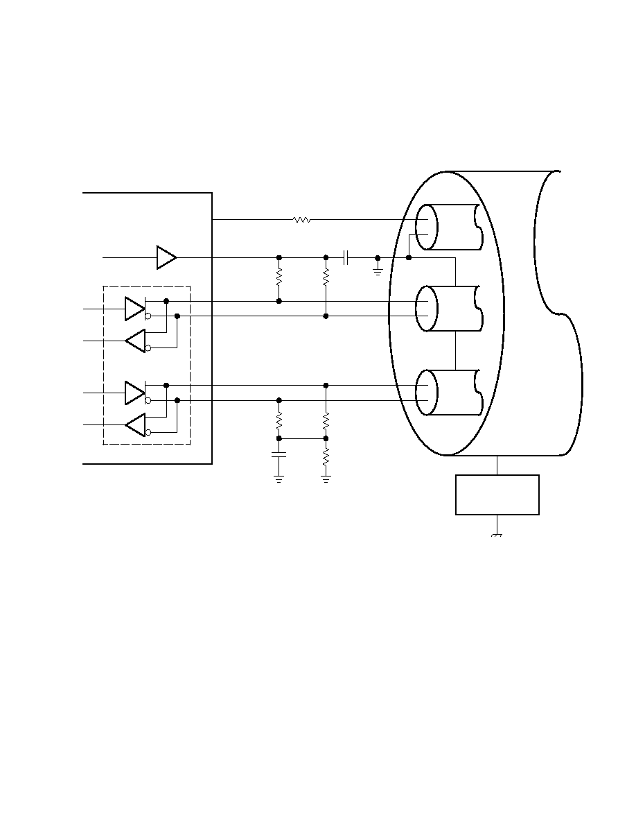
81
8 Application Information
8.1
PHY Port Cable Connection
TPA+
TPA
TPB+
TPB
Cable Port
CPS
TPBIAS
56
56
56
56
5 k
1
µ
F
400 k
220 pF
(see Note A)
TSB43AB22A
Cable
Power
Pair
Cable
Pair
A
Cable
Pair
B
Outer Shield
Termination
NOTE A: IEEE Std 1394-1995 calls for a 250-pF capacitor, which is a nonstandard component value. A 220-pF capacitor is recommended.
Figure 81. TP Cable Connections
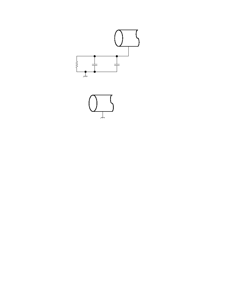
82
1 M
0.001
µ
F
0.01
µ
F
Outer Cable Shield
Chassis Ground
Figure 82. Typical Compliant DC Isolated Outer Shield Termination
Outer Cable Shield
Chassis Ground
Figure 83. Non-DC Isolated Outer Shield Termination
8.2
Crystal Selection
The TSB43AB22A device is designed to use an external 24.576-MHz crystal connected between the XI and XO pins
to provide the reference for an internal oscillator circuit. This oscillator in turn drives a PLL circuit that generates the
various clocks required for transmission and resynchronization of data at the S100 through S400 media data rates.
A variation of less than
±
100 ppm from nominal for the media data rates is required by IEEE Std 1394-1995. Adjacent
PHYs may therefore have a difference of up to 200 ppm from each other in their internal clocks, and PHY devices
must be able to compensate for this difference over the maximum packet length. Large clock variations may cause
resynchronization overflows or underflows, resulting in corrupted packet data.
The following are some typical specifications for crystals used with the PHYs from TI in order to achieve the required
frequency accuracy and stability:
·
Crystal mode of operation: Fundamental
·
Frequency tolerance @ 25
°
C: Total frequency variation for the complete circuit is
±
100 ppm. A crystal with
±
30 ppm frequency tolerance is recommended for adequate margin.
·
Frequency stability (over temperature and age): A crystal with
±
30 ppm frequency stability is recommended
for adequate margin.
NOTE: The total frequency variation must be kept below
±
100 ppm from nominal with some
allowance for error introduced by board and device variations. Trade-offs between frequency
tolerance and stability may be made as long as the total frequency variation is less than
±
100 ppm. For example, the frequency tolerance of the crystal may be specified at 50 ppm and
the temperature tolerance may be specified at 30 ppm to give a total of 80 ppm possible
variation due to the crystal alone. Crystal aging also contributes to the frequency variation.
·
Load capacitance: For parallel resonant mode crystal circuits, the frequency of oscillation is dependent
upon the load capacitance specified for the crystal. Total load capacitance (C
L
) is a function of not only the
discrete load capacitors, but also board layout and circuit. It is recommended that load capacitors with a
maximum of
±
5% tolerance be used.
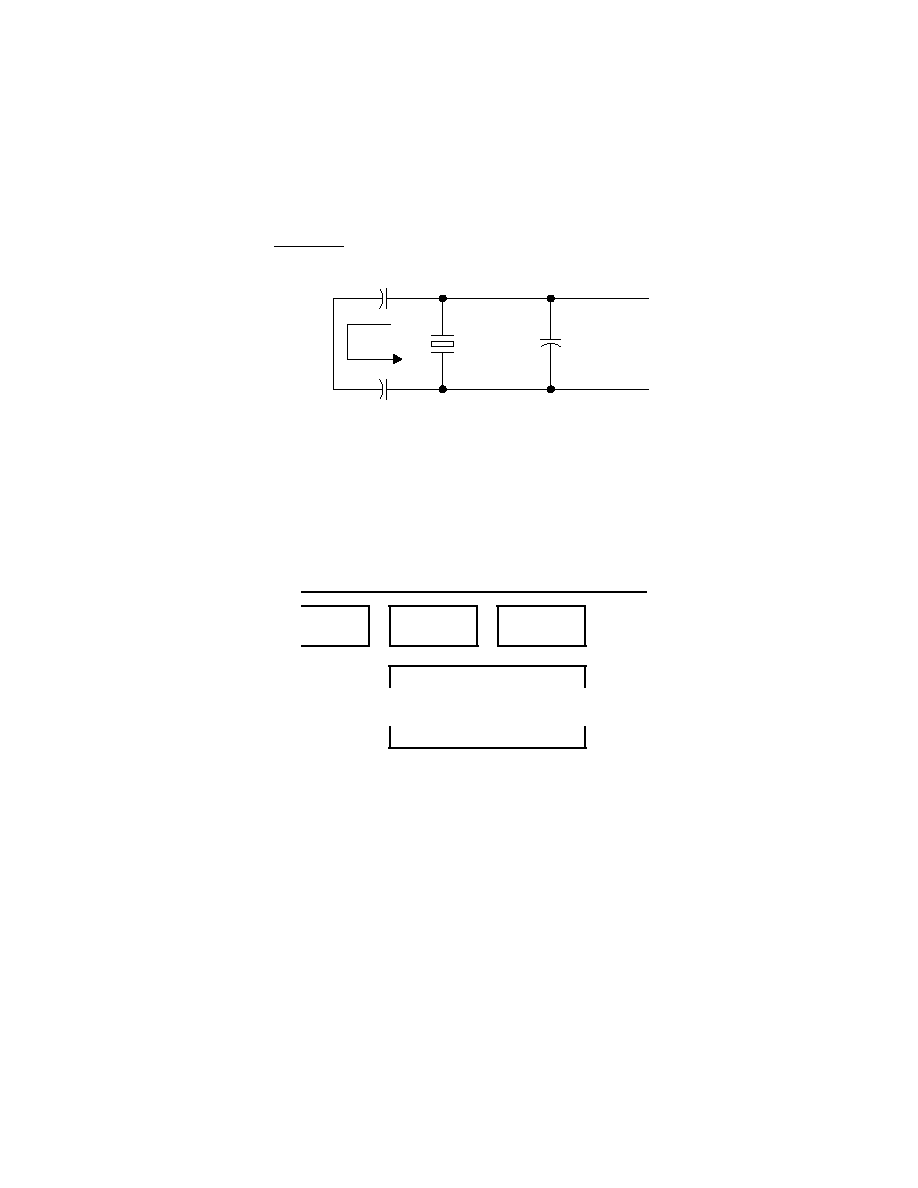
83
For example, load capacitors (C9 and C10 in Figure 84) of 16 pF each were appropriate for the layout of the
TSB43AB22A evaluation module (EVM), which uses a crystal specified for 12-pF loading. The load specified for the
crystal includes the load capacitors (C9 and C10), the loading of the PHY pins (C
PHY
), and the loading of the board
itself (C
BD
). The value of C
PHY
is typically about 1 pF, and C
BD
is typically 0.8 pF per centimeter of board etch; a typical
board can have 3 pF to 6 pF or more. The load capacitors C9 and C10 combine as capacitors in series so that the
total load capacitance is:
C
L
+
C9
C10
C9
)
C10
)
C
PHY
)
C
BD
X1
24.576 MHz
IS
X1
CPHY + CBD
X0
C10
C9
Figure 84. Load Capacitance for the TSB43AB22A PHY
The layout of the crystal portion of the PHY circuit is important for obtaining the correct frequency, minimizing noise
introduced into the PHY phase-lock loop, and minimizing any emissions from the circuit. The crystal and two load
capacitors must be considered as a unit during layout. The crystal and the load capacitors must be placed as close
as possible to one another while minimizing the loop area created by the combination of the three components.
Varying the size of the capacitors may help in this. Minimizing the loop area minimizes the effect of the resonant
current (Is) that flows in this resonant circuit. This layout unit (crystal and load capacitors) must then be placed as
close as possible to the PHY X1 and X0 pins to minimize etch lengths, as shown in Figure 85.
C9
C10
X1
For more details on crystal selection, see application report SLLA051 available from the TI website:
http://www.ti.com/sc/1394.
Figure 85. Recommended Crystal and Capacitor Layout
8.3
Bus Reset
In the TSB43AB22A device, the initiate bus reset (IBR) bit may be set to 1 in order to initiate a bus reset and
initialization sequence. The IBR bit is located in PHY register 1, along with the root-holdoff bit (RHB) and Gap_Count
field, as required by IEEE Std 1394a-2000. Therefore, whenever the IBR bit is written, the RHB and Gap_Count are
also written.
The RHB and Gap_Count may also be updated by PHY-config packets. The TSB43AB22A device is IEEE
1394a-2000 compliant, and therefore both the reception and transmission of PHY-config packets cause the RHB and
Gap_Count to be loaded, unlike older IEEE 1394-1995 compliant PHY devices which decode only received
PHY-config packets.
The gap-count is set to the maximum value of 63 after 2 consecutive bus resets without an intervening write to the
Gap_Count, either by a write to PHY register 1 or by a PHY-config packet. This mechanism allows a PHY-config

84
packet to be transmitted and then a bus reset initiated so as to verify that all nodes on the bus have updated their
RHBs and Gap_Count values, without having the Gap_Count set back to 63 by the bus reset. The subsequent
connection of a new node to the bus, which initiates a bus reset, then causes the Gap_Count of each node to be set
to 63. Note, however, that if a subsequent bus reset is instead initiated by a write to register 1 to set the IBR bit, all
other nodes on the bus have their Gap_Count values set to 63, while this node Gap_Count remains set to the value
just loaded by the write to PHY register 1.
Therefore, in order to maintain consistent gap-counts throughout the bus, the following rules apply to the use of the
IBR bit, RHB, and Gap_Count in PHY register 1:
·
Following the transmission of a PHY-config packet, a bus reset must be initiated in order to verify that all
nodes have correctly updated their RHBs and Gap_Count values and to ensure that a subsequent new
connection to the bus causes the Gap_Count to be set to 63 on all nodes in the bus. If this bus reset is
initiated by setting the IBR bit to 1, the RHB and Gap_Count field must also be loaded with the correct values
consistent with the just transmitted PHY-config packet. In the TSB43AB22A device, the RHB and
Gap_Count are updated to their correct values upon the transmission of the PHY-config packet, so these
values may first be read from register 1 and then rewritten.
·
Other than to initiate the bus reset, which must follow the transmission of a PHY-config packet, whenever
the IBR bit is set to 1 in order to initiate a bus reset, the Gap_Count value must also be set to 63 so as to
be consistent with other nodes on the bus, and the RHB must be maintained with its current value.
·
The PHY register 1 must not be written to except to set the IBR bit. The RHB and Gap_Count must not be
written without also setting the IBR bit to 1.
8.4
EMI Guidelines
For electromagnetic interference (EMI) guidelines and recommendations send a request via e-mail to
1394EMI@list.ti.com.

91
9 Electrical Characteristics
9.1
Absolute Maximum Ratings Over Operating Temperature Ranges
Supply voltage range:
REG18
0.2 V to 2.2 V
. . . . . . . . . . . . . . . . . . . . . . . . . . . . . . . . . . . . . . . . . . . . . . . . . . . . .
AV
DD
0.3 V to 4 V
. . . . . . . . . . . . . . . . . . . . . . . . . . . . . . . . . . . . . . . . . . . . . . . . . . . . . . .
DV
DD
0.3 V to 4 V
. . . . . . . . . . . . . . . . . . . . . . . . . . . . . . . . . . . . . . . . . . . . . . . . . . . . . . .
PLLV
DD
0.3 V to 4 V
. . . . . . . . . . . . . . . . . . . . . . . . . . . . . . . . . . . . . . . . . . . . . . . . . . . . .
V
DDP
0.5 V to 5.5 V
. . . . . . . . . . . . . . . . . . . . . . . . . . . . . . . . . . . . . . . . . . . . . . . . . . . . . .
Input voltage range for PCI, V
I
, PHY, and Miscellaneous
0.5 to V
DD
+ 0.5 V
. . . . . . . . . . . . . . . . . . . . . . . . . .
Output voltage range for PCI, V
O
, PHY, and Miscellaneous
0.5 to V
DD
+ 0.5 V
. . . . . . . . . . . . . . . . . . . . . . . .
Input clamp current, I
IK
(V
I
< 0 or V
I
> V
DD
) (see Note 1)
±
20 mA
. . . . . . . . . . . . . . . . . . . . . . . . . . . . . . . . . . . .
Output clamp current, I
OK
(V
O
< 0 or V
O
> V
DD
) (see Note 2)
±
20 mA
. . . . . . . . . . . . . . . . . . . . . . . . . . . . . . . .
Electrostatic discharge (see Note 3)
HBM: 2 kV, MM: 200 V
. . . . . . . . . . . . . . . . . . . . . . . . . . . . . . . . . . . . . . . . . .
Continuous total power dissipation
See Dissipation Rating Table
. . . . . . . . . . . . . . . . . . . . . . . . . . . . . . . . . . . . .
Operating free-air temperature, T
A
0
°
C to 70
°
C
. . . . . . . . . . . . . . . . . . . . . . . . . . . . . . . . . . . . . . . . . . . . . . . . . . . .
Storage temperature range, T
stg
65
°
C to 150
°
C
. . . . . . . . . . . . . . . . . . . . . . . . . . . . . . . . . . . . . . . . . . . . . . . . . . .
Lead temperature 1,6 mm (1/16 inch) from cage for 10 seconds
260
°
C
. . . . . . . . . . . . . . . . . . . . . . . . . . . . . . .
Stresses beyond those listed under absolute maximum ratings may cause permanent damage to the device. These are stress ratings only, and
functional operation of the device at these or any other conditions beyond those indicated under recommended operating conditions is not implied.
Exposure to absolute-maximum-rated conditions for extended periods may affect device reliability.
NOTES:
1. Applies to external input and bidirectional buffers. For 5-V tolerant use VI > VDDI. For PCI use VI > VDDP.
2. Applies to external output and bidirectional buffers. For 5-V tolerant use VO > VDDI. For PCI use VO > VDDP.
3. HBM is human body model, MM is machine model.
DISSIPATION RATING TABLE
PACKAGE
TA
25
°
C
POWER RATING
DERATING FACTOR§
ABOVE TA = 25
°
C
TA = 70
°
C
POWER RATING
PDT
1.116 W
0.013 W/
°
C
0.563 W
PDT§
0.967 W
0.009 W/
°
C
0.523 W
Standard JEDEC high-K board
§ Standard JEDEC low-K board

92
9.2
Recommended Operating Conditions
TEST
CONDITION
MIN
NOM
MAX
UNIT
REG18
1.6
1.8
2
V
Core voltage, AVDD
3
3.3
3.6
V
Core voltage, DVDD
3
3.3
3.6
V
Core voltage, PLLVDD
2.7
3
3.6
V
Output voltage, VO
TTL and LVCMOS terminals
V
PCI I/O clamping voltage,
VDDP = 3.3 V
3
3.3
3.6
V
PCI I/O clam ing voltage,
VDDP
VDDP = 5 V
4.5
5
5.5
V
PCI
3.3 V
0.475VDDP
VDDP
PCI
5 V
2
VDDP
High-level input voltage, VIH PC(02)
0.7VDD
DVDD
V
High level in ut voltage, VIH
G_RST
0.6VDD
DVDD
Miscellaneous
2
VDDP
PCI
3.3 V
0
0.325VDDP
PCI
5 V
0
0.8
Low-level input voltage, VIL
PC(02)
0
0.2VDD
V
Low level in ut voltage, VIL
G_RST
0
0.3VDD
Miscellaneous
0
0.8
Input voltage V
PCI
3.3 V
0
VDDP
V
Input voltage, VI
Miscellaneous
0
VDDP
V
Output voltage VO§
PCI
3.3 V
0
DVDD
V
Output voltage, VO§
Miscellaneous
0
DVDD
V
Input transition time
(tr and tf), tt
PCI
0
6
ns
Operating free-air
temperature, TA
R
JA = 70.82
°
C/W, TA = 70
°
C
99.3
°
C
Output current, IO
TPBIAS outputs
5.6
1.3
mA
Differential input voltage V
Cable inputs, during data reception
118
260
mV
Differential input voltage, VID
Cable inputs, during arbitration
168
265
mV
Common-mode input voltage,
TPB cable inputs, source power node
0.4706
2.515
V
Common mode in ut voltage,
VIC
TPB cable inputs, nonsource power node
0.4706
2.015¶
V
Maximum junction
128-PDT high-K JEDEC board
R
JA = 74.6
°
C/W, TA = 70
°
C, Pd = 0.6 W
112.1
°
C
Maximum junction
temperature, TJ
128-PDT low-K JEDEC board
R
JA = 101.3
°
C/W, TA = 70
°
C, Pd = 0.6 W
122.8
°
C
Power up reset time, tpu
G_RST input
2
ms
TPA, TPB cable inputs, S100 operation
±
1.08
Receive input jitter
TPA, TPB cable inputs, S200 operation
±
0.5
ns
Receive in ut jitter
TPA, TPB cable inputs, S400 operation
±
0.315
ns
Applies to external inputs and bidirectional buffers without hysteresis.
Miscellaneous terminals are: GPIO2 (90), GPIO3 (89), SDA (92), SCL (91).
§ Applies to external output buffers.
¶ For a node that does not source power; see Section 4.2.2.2 in IEEE Std 1394a-2000.

93
Recommended Operating Conditions (Continued)
TEST
CONDITION
MIN
NOM
MAX
UNIT
R
i
i
t
Between TPA and TPB cable inputs, S100 operation
±
0.8
Receive input
skew
Between TPA and TPB cable inputs, S200 operation
±
0.55
ns
skew
Between TPA and TPB cable inputs, S400 operation
±
0.5
9.3
Electrical Characteristics Over Recommended Operating Conditions
(unless otherwise noted)
PARAMETER
OPERATION
TEST
CONDITIONS
MIN
MAX
UNIT
PCI
IOH = 0.5 mA
0.9VDD
VOH
High-level output voltage
PCI
IOH = 2 mA
2.4
V
VOH
High level out ut voltage
Miscellaneous
IOH = 4 mA
VDD 0.6
V
PCI
IOL = 1.5 mA
0.1VDD
VOL
Low-level output voltage
PCI
IOL = 6 mA
0.55
V
VOL
Low level out ut voltage
Miscellaneous
IOL = 4 mA
0.5
V
IOZ
3-state output high-impedance
Output pins
3.6 V
VO = VDD or GND
±
20
µ
A
I
Low level input current
Input pins
3.6 V
VI = GND
±
20
A
IIL
Low-level input current
I/O pins
3.6 V
VI = GND
±
20
µ
A
IIH
High level input current
PCI
3.6 V
VI = VDD
±
20
µ
A
IIH
High-level input current
Others
3.6 V
VI = VDD
±
20
µ
A
For I/O terminals, input leakage (IIL and IIH) includes IOZ of the disabled output.
Miscellaneous terminals are: GPIO2 (90), GPIO3 (89), SDA (92), SCL (91).

94
9.4
Electrical Characteristics Over Recommended Ranges of Operating Conditions
(unless otherwise noted)
9.4.1
Device
PARAMETER
TEST CONDITIONS
MIN
TYP
MAX
UNIT
S
l
t (i t
l
lt
l t
bl d
See Note 4
92.4
IDD
Supply current (internal voltage regulator enabled,
REG EN = L)
See Note 5
81.2
mA
IDD
REG_EN = L)
See Note 6
76.8
mA
S
l
t (REG EN
H
t
l 1 8 V
li d
See Note 4
85.5
IDD
Supply current (REG_EN = H, external 1.8 V supplied
to REG18)
See Note 5
74.1
mA
IDD
to REG18)
See Note 6
69.8
mA
IDD(ULP)
Supply current--ultralow power mode (internal voltage
regulator enabled, REG_EN = L)
Ports disabled
VDD = 1.8 V (internal)
TA = 25
°
C
3
mA
IDD(ULP)
Supply current--ultralow power mode (internal voltage
regulator disabled, REG_EN = H, REG18 = 1.8 V)
Ports disabled
VDD = 1.8 V (external)
TA = 25
°
C
1.8
mA
VTH
Power status threshold, CPS input
400-k
resistor
4.7
7.5
V
VO
TPBIAS output voltage
At rated IO current
1.665
2.015
V
II
Input current (PC0 PC2 inputs)
VDD = 3.6 V
5
µ
A
I
Pullup current (G RST input)
VI = 1.5 V
90
20
A
IIRST
Pullup current (G_RST input)
VI = 0 V
90
20
µ
A
Measured at cable power side of resistor.
NOTES:
4. Transmit (all ports transmit, 100% bandwidth, S400), VDD = 3.3 V, TA = 25
°
C
5. Repeat data (receive on one port, transmit on other port, full isochronous payload of 84
µ
s, S400, data value of CCCC CCCCh),
VDD = 3.3 V, TA = 25
°
C
6. Idle (receive cycle start on one port, transmit cycle start on other port), VDD = 3.3 V, TA = 25
°
C
9.4.2
Driver
PARAMETER
TEST CONDITIONS
MIN
MAX
UNIT
VOD
Differential output voltage
56
, see Figure 91
172
265
mV
IDIFF
Driver difference current, TPA+, TPA, TPB+, TPB
Drivers enabled, speed signaling off
1.05
1.05
mA
ISP200
Common-mode speed signaling current, TPB+, TPB
S200 speed signaling enabled
4.84§
2.53§
mA
ISP400
Common-mode speed signaling current, TPB+, TPB
S400 speed signaling enabled
12.4§
8.1§
mA
VOFF
Off state differential voltage
Drivers disabled, see Figure 91
20
mV
Limits defined as algebraic sum of TPA+ and TPA driver currents. Limits also apply to TPB+ and TPB algebraic sum of driver currents.
§ Limits defined as absolute limit of each of TPB+ and TPB driver currents.
TPAx+
TPBx+
TPAx
TPBx
56
Figure 91. Test Load Diagram

95
9.4.3
Receiver
PARAMETER
TEST CONDITIONS
MIN
TYP
MAX
UNIT
Z
Differential impedance
Drivers disabled
4
7
k
ZID
Differential impedance
Drivers disabled
4
pF
Z
Common mode impedance
Drivers disabled
20
k
ZIC
Common-mode impedance
Drivers disabled
24
pF
VTH-R
Receiver input threshold voltage
Drivers disabled
30
30
mV
VTH-CB
Cable bias detect threshold, TPBx cable inputs
Drivers disabled
0.6
1
V
VTH+
Positive arbitration comparator threshold voltage
Drivers disabled
89
168
mV
VTH
Negative arbitration comparator threshold voltage
Drivers disabled
168
89
mV
VTHSP200
Speed signal threshold
TPBIASTPA common mode
voltage, drivers disabled
49
131
mV
VTHSP400
Speed signal threshold
TPBIASTPA common mode
voltage, drivers disabled
314
396
mV
9.5
Thermal Characteristics
PARAMETER
TEST CONDITIONS
MIN
TYP
MAX
UNIT
128-PDT
R
JA, high-K board
74.6
°
C/W
128-PDT
R
JA, low-K board
Board mounted, no air flow, JEDEC test board
101.3
°
C/W
128-PDT
R
JC
,
,
18.7
°
C/W
9.6
Switching Characteristics for PHY Port Interface
PARAMETER
TEST CONDITIONS
MIN
TYP
MAX
UNIT
Jitter, transmit
Between TPA and TPB
±
0.15
ns
Skew, transmit
Between TPA and TPB
±
0.1
ns
tr
TP differential rise time, transmit
10% to 90%, at 1394 connector
0.5
1.2
ns
tf
TP differential fall time, transmit
90% to 10%, at 1394 connector
0.5
1.2
ns
9.7
Operating, Timing, and Switching Characteristics of XI
PARAMETER
MIN
TYP
MAX
UNIT
VDD
3
3.3
3.6
V (PLLVDD)
VIH
High-level input voltage
0.63 VDD
V
VIL
Low-level input voltage
0.33 VDD
V
Input clock frequency
24.576
MHz
Input clock frequency tolerance
<100
PPM
Input slew rate
0.2
4
V/ns
Input clock duty cycle
40%
60%
9.8
Switching Characteristics for PCI Interface
PARAMETER
MEASURED
MIN
TYP
MAX
UNIT
tsu
Setup time before PCLK
50% to 50%
7
ns
th
Hold time before PCLK
50% to 50%
0
ns
tval
Delay time, PCLK to data valid
50% to 50%
2
11
ns
These parameters are ensured by design.
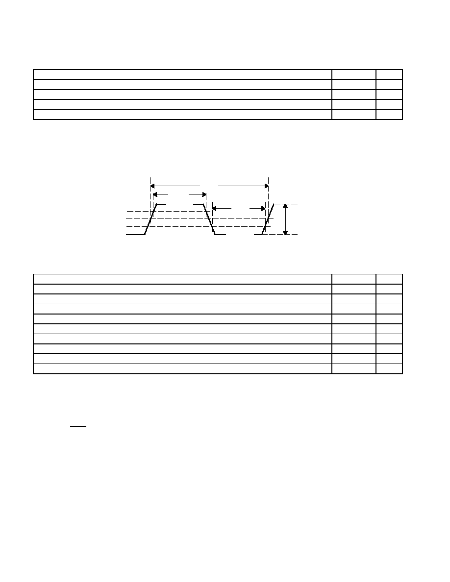
96
9.8.1
CardBus PC Card Clock Specifications
PARAMETER
MIN
MAX
UNIT
tcyc
CCLK cycle time (see Note 7)
30
R
ns
thigh
CCLK high time
12
ns
tlow
CCLK low time
12
ns
CCLK slew rate (see Note 8)
1
4
V/ns
NOTES:
7. In general, all CardBus PC Card components must work with any clock frequency up to 33 MHz. The clock frequency may be
changed at any time during the operation of the system so long as the clock edges remain clean (monotonic) and the minimum cycle
and high and low times are not violated. If the clock is stopped, it must be in a low state. A variance on this specification is allowed
for the CardBus PC Card adapter which may operate the CardBus PC Card interface at any single fixed frequency up to 33 MHz,
and may enforce a policy of no frequency changes.
8. Rise and fall times are specified in terms of the edge rate measured in V/ns. This slew rate must be met across the minimum
peak-to-peak portion of the clock waveform (see Figure 92).
0.4 VCC, p-to-p
(Minimum)
0.325 VCC
0.4 VCC
0.475 VCC
0.2 VCC
0.6 VCC
tlow
thigh
tcyc
Figure 92. CardBus PC Card Clock Waveform
9.8.2
3.3-V Timing Parameters
MIN
MAX
UNIT
tval
CCLK-to-signal-valid delay (see Notes 9 and 10)
2
18
ns
ton
Float-to-active delay (see Note 9)
2
ns
toff
Active-to-float delay (see Note 9)
28
ns
tsu
Input set up time to CCLK (see Note 11)
7
ns
th
Input hold time from CCLK (see Note 11)
0
ns
trst
Reset active time after power stable (see Note 12)
1
ms
trst-clk Reset active time after CCLK stable (see Note 12)
100
clocks
trst-off
Reset-active-to-output-float delay (see Notes 12 and 13)
40
ns
tpulse
CSTSCHG remote wakeup pulse width (see Note 14)
1
ms
NOTES:
9. tval includes the time to propagate data from internal registers to the output buffer and drive the output to a valid level. Minimum tval
is measured from CCLK crossing Vtest to the signal crossing VIH on falling edges and VIL on rising edges. Maximum tval is measured
from CCLK crossing Vtest to the signal's last transition out of the threshold region (VIL for falling edges, VIH for rising edges).
10. Minimum times are specified with 0-pF equivalent load; maximum times are specified with 30-pF equivalent load. Actual test
capacitance may vary, but results must be correlated to these specifications. Systems which exceed this capacitance, due to long
traces between the socket and adaptor, must reduce the CCLK frequency appropriately.
11. tsu and th are measured at VTH for rising edges and VTL for falling edges.
12. CRST is asserted asynchronously and negated synchronously with respect to CCLK. CCLK Stable means that Vcc is within
tolerances and CCLK is meeting specifications.
13. See PC Card Standard-- Electrical Specification for the CardBus PC Card and adapter signals which must be in a high-impedance
state.
14. This parameter only applies when signaling remote wakeup over the CSTSCHG terminal. All other status change information must
be signaled by asserting CSTSCHG until the resultant interrupt is serviced.
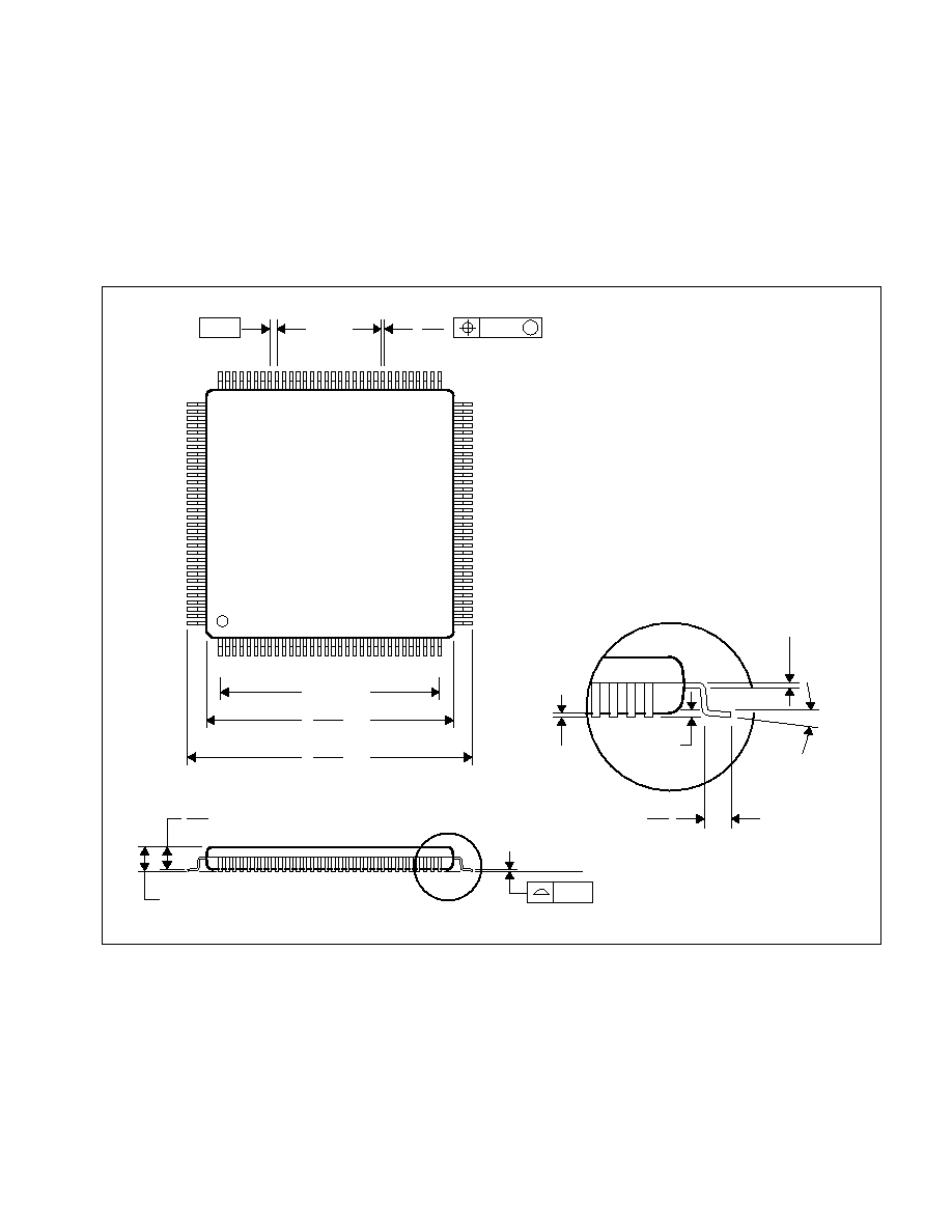
101
10 Mechanical Information
The TSB43AB22A device is packaged in a 128-terminal PDT package. The following shows the mechanical
dimensions for the PDT package.
PDT (S-PQFP-G128)
PLASTIC QUAD FLATPACK
64
33
0,13 NOM
Gage Plane
0,25
0,45
0,75
Seating Plane
0,05 MIN
4087726/A 11/95
0,23
0,13
65
32
96
1
12,40 TYP
128
97
SQ
SQ
0,95
1,05
15,90
16,10
13,95
1,20 MAX
14,05
0,08
0,40
M
0,05
0
°
5
°
NOTES: A. All linear dimensions are in millimeters.
B. This drawing is subject to change without notice.
C. Falls within JEDEC MO-136

102