 | –≠–ª–µ–∫—Ç—Ä–æ–Ω–Ω—ã–π –∫–æ–º–ø–æ–Ω–µ–Ω—Ç: TPS2201 | –°–∫–∞—á–∞—Ç—å:  PDF PDF  ZIP ZIP |

TPS2201, TPS2201Y
DUAL-SLOT PC CARD POWER-INTERFACE SWITCHES
FOR PARALLEL PCMCIA CONTROLLERS
SLVS094B ≠ AUGUST 1994 ≠ REVISED AUGUST 1995
Copyright
©
1995, Texas Instruments Incorporated
6≠1
POST OFFICE BOX 655303
∑
DALLAS, TEXAS 75265
∑
Fully Integrated V
CC
and V
pp
Switching for
Dual-Slot PC Card Interface
∑
Compatible With Controllers From Cirrus,
Intel, and Texas Instruments
∑
Meets PCMCIA Standards
∑
Internal Charge Pump (No External
Capacitors Required) ≠ 12-V Supply Can Be
Disabled Except for Programming
∑
Short Circuit and Thermal Protection
∑
Space Saving SSOP (DB) Package
∑
Compatible With 3.3-V, 5-V and 12-V PC
Cards
∑
Power Saving I
DD
= 83
µ
A Typ, I
Q
= 1
µ
A
∑
Low r
DS(on)
(160-m
V
CC
Switch)
∑
Break-Before-Make Switching
description
The TPS2201 PC Card (PCMCIA) power interface switch provides an integrated power-management solution
for two PC Cards. All of the discrete power MOSFETs, a logic section, current limiting, thermal protection, and
power-good reporting for PC Card control are combined on a single integrated circuit (IC), using Texas
Instruments LinBiCMOS
TM
process. The circuit allows the distribution of 3-V, 5-V and/or 12-V card power and
is compatible with most PCMCIA controllers. The current-limiting feature eliminates the need for fuses, which
reduces component count and improves reliability; current-limit reporting can help the user isolate a system fault
to a bad card.
The TPS2201 maximizes battery life by generating its own switch-drive voltage using an internal charge pump.
Therefore, the 12-V supply can be powered down and only brought out of standby when flash memory needs
to be written to or erased. End equipment for the TPS2201 includes notebook computers, desktop computers,
personal digital assistants (PDAs), digital cameras, handiterminals, and bar-code scanners.
typical PC card power distribution application
CPU
PCMCIA
Controller
12 V
Power Supply
Vpp1
Vpp2
VCC
VCC
PC
Card A
VDD
TPS2201
5 V
3 V
SHDN
BPWR_GOOD
OC
Control Lines
8
Vpp1
Vpp2
VCC
VCC
PC
Card B
12V
5V
3V
AVPP
AVCC
AVCC
BVPP
BVCC
BVCC
APWR_GOOD
BVCC
AVCC
LinBiCMOS is a trademark of Texas Instruments Incorporated.
1
2
3
4
5
6
7
8
9
10
11
12
13
14
15
30
29
28
27
26
25
24
23
22
21
20
19
18
17
16
5V
5V
A_VPP_PGM
A_VPP_VCC
A_VCC5
A_VCC3
12V
AVPP
AVCC
AVCC
AVCC
GND
APWR_GOOD
SHDN
3V
5V
B_VPP_PGM
B_VPP_VCC
B_VCC5
B_VCC3
V
DD
12V
BVPP
BVCC
BVCC
BVCC
BPWR_GOOD
OC
3V
3V
DB OR DF PACKAGE
(TOP VIEW)
PRODUCTION DATA information is current as of publication date.
Products conform to specifications per the terms of Texas Instruments
standard warranty. Production processing does not necessarily include
testing of all parameters.
TPS2201, TPS2201Y
DUAL-SLOT PC CARD POWER-INTERFACE SWITCHES
FOR PARALLEL PCMCIA CONTROLLERS
SLVS094B ≠ AUGUST 1994 ≠ REVISED AUGUST 1995
6≠2
POST OFFICE BOX 655303
∑
DALLAS, TEXAS 75265
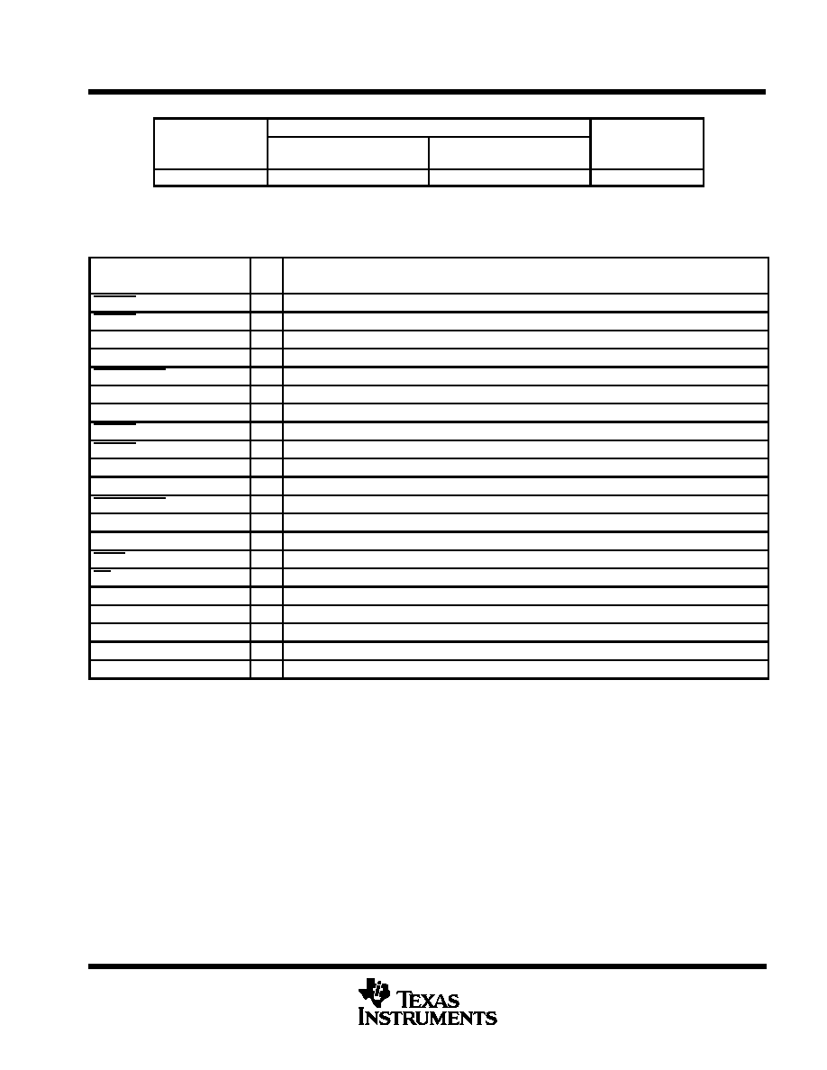
AVAILABLE OPTIONS
PACKAGED DEVICES
CHIP FORM
TJ
SHINK SMALL-OUTLINE
(DB)
SMALL-OUTLINE
(DF)
CHIP FORM
(Y)
≠ 40
∞
C to 150
∞
C
TPS2201IDB
TPS2201IDF
TPS2201Y
The DF package is only available left-end taped and reeled (indicated by the LE suffix on the device type; e.g.,
TPS2201IDFLE).
Terminal Functions
TERMINAL
I/O
DESCRIPTION
NAME
NO.
I/O
DESCRIPTION
A_VCC3
6
I
Logic input that controls voltage on AVCC (see control-logic table)
A_VCC5
5
I
Logic input that controls voltage on AVCC (see control-logic table)
A_VPP_PGM
3
I
Logic input that controls voltage on AVPP (see control-logic table)
A_VPP_VCC
4
I
Logic input that controls voltage on AVPP (see control-logic table)
APWR_GOOD
13
O
Logic-level power-ready output that stays low as long as AVPP is within limits
AVCC
9, 10, 11
O
Switched output that delivers 0 V, 3.3 V, 5 V, or high impedance
AVPP
8
O
Switched output that delivers 0 V, 3.3 V, 5 V, 12 V, or high impedance
B_VCC3
26
I
Logic input that controls voltage on BVCC (see control-logic table)
B_VCC5
27
I
Logic input that controls voltage on BVCC (see control-logic table)
B_VPP_PGM
29
I
Logic input that controls voltage on BVPP (see control-logic table)
B_VPP_VCC
28
I
Logic input that controls voltage on BVPP (see control-logic table)
BPWR_GOOD
19
O
Logic-level power-ready output that stays low as long as BVPP is within limits
BVCC
20, 21, 22
O
Switched output that delivers 0 V, 3.3 V, 5 V, or high impedance
BVPP
23
O
Switched output that delivers 0 V, 3.3 V, 5 V, 12 V, or high impedance
SHDN
14
I
Logic input that shuts down the TPS2201 and set all power outputs to high-impedance state
OC
18
O
Logic-level overcurrent reporting output that goes low when an overcurrent condition exists
VDD
25
5-V power to chip
GND
12
Ground
3V
15, 16, 17
I
3-V VCC input for card power
5V
1, 2, 30
I
5-V VCC input for card power
12V
7, 24
I
12-V VPP input for card power

TPS2201, TPS2201Y
DUAL-SLOT PC CARD POWER-INTERFACE SWITCHES
FOR PARALLEL PCMCIA CONTROLLERS
SLVS094B ≠ AUGUST 1994 ≠ REVISED AUGUST 1995
6≠3
POST OFFICE BOX 655303
∑
DALLAS, TEXAS 75265
TPS2201Y chip information
This chip, when properly assembled, displays characteristics similar to the TPS2201. Thermal compression or
ultrasonic bonding may be used on the doped aluminum bonding pads. The chip may be mounted with
conductive epoxy or a gold-silicon preform.
BONDING PAD ASSIGNMENTS
CHIP THICKNESS: 15 MILS TYPICAL
BONDING PADS: 4
◊
4 MILS MINIMUM
TJmax = 150
∞
C
TOLERANCES ARE
±
10%
ALL DIMENSIONS ARE IN MILS
204
142
TPS2201Y
(2)
(28)
(1)
(3)
(29)
(30)
(27)
(4)
5V
5V
5V
A_VPP_PGM
A_VPP_VCC
B_VPP_PGM
B_VPP_VCC
B_VCC5
(6)
(5)
(7)
(8)
A_VCC5
A_VCC3
12V
AVPP
(10)
(9)
(11)
(12)
AVCC
AVCC
AVCC
GND
(14)
(13)
(15)
APWR_GOOD
SHDN
3V
(24)
(25)
(26)
(23)
B_VCC3
VDD
12V
BVPP
(20)
(21)
(22)
(19)
BVCC
BVCC
BVCC
BPWR_GOOD
(16)
(17)
(18)
OC
3V
3V
(2)
(1)
(3)
(4)
(6)
(5)
(7)
(8)
(10)
(9)
(11)
(12)
(14)
(13)
(15)
(20)
(21)
(22)
(19)
(16)
(17)
(18)
(28)
(29)
(30)
(27)
(24)
(25)
(26)
(23)

TPS2201, TPS2201Y
DUAL-SLOT PC CARD POWER-INTERFACE SWITCHES
FOR PARALLEL PCMCIA CONTROLLERS
SLVS094B ≠ AUGUST 1994 ≠ REVISED AUGUST 1995
6≠4
POST OFFICE BOX 655303
∑
DALLAS, TEXAS 75265
absolute maximum ratings over operating free-air temperature (unless otherwise noted)
Supply voltage range, V
DD
≠ 0.3 V to 7 V
. . . . . . . . . . . . . . . . . . . . . . . . . . . . . . . . . . . . . . . . . . . . . . . . . . . . . . . . . .
Input voltage range for card power: V
I(5V)
≠ 0.3 V to 7 V
. . . . . . . . . . . . . . . . . . . . . . . . . . . . . . . . . . . . . . . . . . . . .
V
I(3V)
≠ 0.3 V to V
I(5V)
. . . . . . . . . . . . . . . . . . . . . . . . . . . . . . . . . . . . . . . . . . .
V
I(12V)
≠ 0.3 V to 14 V
. . . . . . . . . . . . . . . . . . . . . . . . . . . . . . . . . . . . . . . . . . .
Logic input voltage
≠ 0.3 V to 7 V
. . . . . . . . . . . . . . . . . . . . . . . . . . . . . . . . . . . . . . . . . . . . . . . . . . . . . . . . . . . . . . . . .
Continuous total power dissipation
See Dissipation Rating Table
. . . . . . . . . . . . . . . . . . . . . . . . . . . . . . . . . . . . .
Output current (each card): I
O(xVCC)
internally limited
. . . . . . . . . . . . . . . . . . . . . . . . . . . . . . . . . . . . . . . . . . . . .
I
O(xVPP)
internally limited
. . . . . . . . . . . . . . . . . . . . . . . . . . . . . . . . . . . . . . . . . . . . .
Operating virtual junction temperature range, T
J
≠ 40
∞
C to 150
∞
C
. . . . . . . . . . . . . . . . . . . . . . . . . . . . . . . . . . . .
Operating free-air temperature range, T
A
≠ 40
∞
C to 85
∞
C
. . . . . . . . . . . . . . . . . . . . . . . . . . . . . . . . . . . . . . . . . . . .
Storage temperature range, T
stg
≠ 55
∞
C to 150
∞
C
. . . . . . . . . . . . . . . . . . . . . . . . . . . . . . . . . . . . . . . . . . . . . . . . . .
Lead temperature 1,6 mm (1/16 inch) from case for 10 seconds
260
∞
C
. . . . . . . . . . . . . . . . . . . . . . . . . . . . . . .
Stresses beyond those listed under "absolute maximum ratings" may cause permanent damage to the device. These are stress ratings only, and
functional operation of the device at these or any other conditions beyond those indicated under "recommended operating conditions" is not
implied. Exposure to absolute-maximum-rated conditions for extended periods may affect device reliability.
DISSIPATION RATING TABLE
PACKAGE
TA
25
∞
C
POWER RATING
DERATING FACTOR
ABOVE TA = 25
∞
C
TA = 70
∞
C
POWER RATING
TA = 85
∞
C
POWER RATING
DB
1024 mW
8.2 mW/
∞
C
655 mW
532 mW
DF
1158 mW
9.26 mW/
∞
C
741 mW
602 mW
Maximum values are calculated using a derating factor based on R
JA = 108
∞
C/ W for the package.
These devices are mounted on an FR4 board with no special thermal considerations.
recommended operating conditions
MIN
MAX
UNIT
Supply voltage, VDD
4.75
5.25
V
VI(5V)
0
5.25
V
Input voltage range, VI
VI(3V)
0
VI(5V)
V
VI(12V)
0
13.5
V
Output current IO
IO(xVCC) at 25
∞
C
1
A
Output current, IO
IO(xVPP) at 25
∞
C
150
mA
Operating virtual junction temperature, TJ
≠ 40
125
∞
C
VI(3 V) should not be taken above VI(5 V).

TPS2201, TPS2201Y
DUAL-SLOT PC CARD POWER-INTERFACE SWITCHES
FOR PARALLEL PCMCIA CONTROLLERS
SLVS094B ≠ AUGUST 1994 ≠ REVISED AUGUST 1995
6≠5
POST OFFICE BOX 655303
∑
DALLAS, TEXAS 75265
electrical characteristics, T
A
= 25
∞
C, V
DD
= 5 V (unless otherwise noted)
dc characteristics
PARAMETER
TEST CONDITIONS
TPS2201
UNIT
PARAMETER
TEST CONDITIONS
MIN
TYP
MAX
UNIT
5 V to xVCC
160
m
3 V to xVCC
225
m
Switch resistances
5 V to xVPP
6
3 V to xVPP
6
12 V to xVPP
1
Clamp low voltage
Ipp at 10 mA
0.8
V
Clamp low voltage
ICC at 10 mA
0.8
V
I
High impedance state
TA = 25
∞
C
1
10
Leakage current
Ipp High-impedance state
TA = 85
∞
C
50
µ
A
Leakage current
ICC High impedance state
TA = 25
∞
C
1
10
µ
A
ICC High-impedance state
TA = 85
∞
C
50
Input current
IDD
VO(AVCC) = VO(BVCC) = 5 V,
VO(AVPP) = VO(BVPP) = 12 V
83
150
µ
A
Input current
IDD in shutdown
VO(BVCC) = VO(AVCC) = VO(AVPP)
= VO(BVPP) = high Z
1
µ
A
Power-ready threshold, PWR_GOOD
10.72
11.05
11.4
V
Power-ready hysteresis, PWR_GOOD (12-V mode)
50
mV
Short-circuit output-
IO(xVCC)
TJ = 85
∞
C
Output shorted to GND
0.75
1.3
1.9
A
current limit
IO(xVPP)
TJ = 85
∞
C, Output shorted to GND
120
200
400
mA
logic section
PARAMETER
TEST CONDITIONS
TPS2201
UNIT
PARAMETER
TEST CONDITIONS
MIN
MAX
UNIT
Logic input current
1
µ
A
Logic input high level
2.7
V
Logic input low level
0.8
V
Logic output high level
IO = 1 mA
VDD ≠ 0.4
V
Logic output low level
IO = 1 mA
0.4
V
switching characteristics
PARAMETER
TEST CONDITIONS
TPS2201
UNIT
PARAMETER
TEST CONDITIONS
MIN
TYP
MAX
UNIT
t
Output rise time
VO(xVCC)
1.2
ms
tr
Output rise time
VO(xVPP)
5
ms
tf
Output fall time
VO(xVCC)
10
ms
tf
Output fall time
VO(xVPP)
14
ms
VI( VPP PGM) to VO( VPP)
ton
5.8
ms
VI(x_VPP_PGM) to VO(xVPP)
toff
18
ms
t d
Propagation delay (see Figure 1)
V (
CC ) to xVCC (3 V)
ton
5.8
ms
tpd
Propagation delay (see Figure 1)
VI(x_VCC3) to xVCC (3 V)
toff
28
ms
VI( VCC5) to xVCC (5 V)
ton
4
ms
VI(x_VCC5) to xVCC (5 V)
toff
30
ms
Refer to Parameter Measurement Information
Rise and fall times are with CL = 100
µ
F.