 | –≠–ª–µ–∫—Ç—Ä–æ–Ω–Ω—ã–π –∫–æ–º–ø–æ–Ω–µ–Ω—Ç: TMS320C5x | –°–∫–∞—á–∞—Ç—å:  PDF PDF  ZIP ZIP |
Document Outline
- Features
- description
- Pin Functions for Devices in the PQ Package
- Pin Functions for the TMS320LC57 in the PBK Package
- Pin Functions for Devices in the PZ Package
- Pin Functions for the TMS320C52, TMS320LC52 in the PJ Package
- Pin Functions for the TMS320C57S, TMS320LC57S in the PGE Package
- architecture
- functional block diagram
- 32-bit ALU/accumulator
- scaling shifters
- parallel logic unit
- 16-bit parallel multiplier
- auxiliary registers and auxiliary-register arithmetic unit (ARAU)
- memory
- interrupts and subroutines
- power-down modes
- bus-keeper circuitry (TMS320LC56/êC57S/êLC57)
- external interface
- external direct-memory access (DMA) capability
- host port interface (HPI) (TMS320C57S, TMS320LC57, TMS320LC57S only)
- serial ports
- software wait-state generators
- timer
- IEEE 1149.1 boundary scan interface
- on-chip analysis block
- multiprocessing
- instruction set
- addressing modes
- repeat feature
- instruction set summary
- instruction set summary (continued)
- development support
- Software Development Tools:
- Hardware Development Tools:
- device and development support tool nomenclature
- TMX
- TMP
- TMS
- TMDX
- TMDS
- documentation support
- absolute maximum ratings over operating ambient-air temperature range (unless otherwise noted) (ê 320C5x only)Å
- recommended operating conditions (ê320C5x only)
- electrical characteristics over recommended ranges of supply voltage and operating ambient-air temperature ( unless otherwise noted) (ê 320C5x only)
- absolute maximum ratings over specified temperature range (unless otherwise noted) (ê320LC5x only)Å
- recommended operating conditions (ê320LC5x only)
- electrical characteristics over recommended ranges of supply voltage and operating free-air temperature ( unless otherwise noted) (ê 320LC5x only)
- PARAMETER MEASUREMENT INFORMATION
- signal transition levels
- timing parameter symbology
- CLOCK CHARACTERISTICS AND TIMING
- internal divide-by-two clock option with external crystal
- recommended operating conditions for internal divide-by-two clock option
- external divide-by-two clock option
- switching characteristics over recommended operating conditions [ H = 0.5 tc(CO)] (ê320C5x only) (see Figure 13)
- switching characteristics over recommended operating conditions [ H = 0.5 tc(CO)] (ê320LC5x only) (see Figure 13)
- PLL clock generator option
- switching characteristics over recommended operating conditions [H = 0.5 tc(CO)] (ê320C5x only) (see Figure 14)
- switching characteristics over recommended operating conditions [ H = 0.5 tc(CO)] (ê320C5x only) (see Figure 14)
- MEMORY AND PARALLEL I/O INTERFACE READ
- switching characteristics over recommended operating conditions [H = 0.5tc(CO) (ê320C5x only) (see Figure 15)
- switching characteristics over recommended operating conditions [H = 0.5 tc(CO)] ('320LC5x only) (see figure 15)
- timing requirements over recommended ranges of supply voltage and operating ambient-air temperature [H=0.5tc(CO)] ('320C5x only) (see Figure 15)
- timing requirements over recommended ranges of supply voltage and operating ambient-air temperature [H=0.5tc(CO)] ('320C5x only) (see Figure 15)
- MEMORY AND PARALLEL I/O INTERFACE WRITE
- switching characteristics over recommended operating conditions [H = 0.5tc(CO)] ('320C5x only) (see Figure 15)
- switching characteristics over recommended operating conditions [H =0.5tc(CO)] ('320C5x only) (see Figure 15)
- READY TIMING FOR EXTERNALLY-GENERATED WAIT STATES
- tining requirements over recommended ranges of supply voltage and operating ambient-air temperature (see Note 5) See Figure 18)
- RESET, INTERRUPT, AND BIO
- timing requirements over recommended ranges of supply voltage and operating ambient-air temperature [H=0.5tc(CO)] (see Figure 19)
- INSTRUCTION ACQUISITION (IAQ), INTERRUPT ACKNOWLEDGE (IACK), EXTERNAL FLAG ( XF), AND TOUT ( SEE NOTE 6)
- switching characteristics over recommended operating conditions [H=0.5tc(CO)] (see Figure 20)
- EXTERNAL DMA
- switching characteristics over recommended operating conditions [H = 0.5tc(CO)] (see Note 7) (see Figure 21)
- SERIAL-PORT RECEIVE TIMING
- timing requirements over recommended ranges of supply voltage and operating ambient-air temperature [H=0.5tc(CO)] (see Figure 22)
- SERIAL-PORT TRANSMIT TIMING, EXTERNAL CLOCKS, AND EXTERNAL FRAMES
- switching characteristics over recommended operating conditions (see Note 8) (see Fihure 23)
- timing requirements over recommended ranges of supply voltage and operating ambient-air temperature [H=0.5tc(CO)] (see Note 8) (see Fihure 23)
- SERIAL-PORT TRANSMIT TIMING, INTERNAL CLOCKS, AND INTERNAL FRAMES ( SEE NOTE 8)
- switching characteristics over recommended operating conditions [H = 0.5tc(CO)] (see Figure 24)
- SERIAL-PORT RECEIVE TIMING IN TDM MODE
- timing requirements over recommended ranges of supply voltage and operating ambient-air temperature [H=0.5tc(CO)] (see Figure 25)
- SERIAL-PORT TRANSMIT TIMING IN TDM MODE
- switching characteristics over recommended operating conditions [H = 0.5tc(CO)] (see Figure 26)
- timing requirements over recommended ranges of supply voltage and operating ambient-air temperature [H=0.5tc(CO)] (see Figure 26)
- BUFFERED SERIAL-PORT RECEIVE TIMING
- timing requirements over recommended ranges of supply voltage and operating ambient-air temperature [H=0.5tc(CO)] (see Figure 27)
- BUFFERED SERIAL-PORT TRANSMIT TIMING OF EXTERNAL FRAMES (SEE NOTES 9 AND 10)
- switching characteristics over recommended operating conditions (see Figure 28)
- timing requirements over recommended operating conditions (see Figure 28)
- BUFFERED SERIAL-PORT TRANSMIT TIMING OF INTERNAL FRAME AND INTERNAL CLOCK ( SEE NOTES 9 AND 10)
- switching characteristics over recommended operating conditions [H = 0.5tc(CO)] (see Figure 29)
- HOST PORT INTERFACE (TMS320C57S, TMS320LC57 ONLY)
- switching characteristics over recommended operating conditions [ H = 0.5tc(CO)] (see Notes 11 and 12) (see Figure 30 through Figure 33)
- timing requirements over recommended operating conditions [H =0.5tc(CO)] (See Note 11) (see Figure 30 through Figure 33)
- MECHANICAL DATA
- PQ(S-PQFP-G132) PLASTIC QUAD FLATPACK
- PBK(S-PQFP-G128) PLSTIC QUAD FLATPACK
- PJ (R-PQFP-G100) PLASTIC QUAD FLATPACK
- PZ (S-PQFP-G100) PLASTIC QUAD FLATPACK
- PGE (S-PQFP-G144) PLASTIC QUAD FLATPACK

TMS320C5x, TMS320LC5x
DIGITAL SIGNAL PROCESSORS
SPRS030A ≠ APRIL 1995 ≠ REVISED APRIL 1996
1
POST OFFICE BOX 1443
∑
HOUSTON, TEXAS 77251≠1443
D
Powerful 16-Bit TMS320C5x CPU
D
20-, 25-, 35-, and 50-ns Single-Cycle
Instruction Execution Time for 5-V
Operation
D
25-, 40-, and 50-ns Single-Cycle Instruction
Execution Time for 3-V Operation
D
Single-Cycle 16
◊
16-Bit Multiply/Add
D
224K
◊
16-Bit Maximum Addressable
External Memory Space (64K Program, 64K
Data, 64K I/O, and 32K Global)
D
2K, 4K, 8K, 16K, 32K
◊
16-Bit Single-Access
On-Chip Program ROM
D
1K, 3K, 6K, 9K
◊
16-Bit Single-Access
On-Chip Program / Data RAM (SARAM)
D
1K Dual-Access On-Chip Program / Data
RAM (DARAM)
D
Full-Duplex Synchronous Serial Port for
Coder /Decoder Interface
D
Time-Division-Multiplexed (TDM) Serial Port
D
Hardware or Software Wait-State
Generation Capability
D
On-Chip Timer for Control Operations
D
Repeat Instructions for Efficient Use of
Program Space
D
Buffered Serial Port
D
Host Port Interface
D
Multiple Phase-Locked Loop (PLL)
Clocking Options (
◊
1,
◊
2,
◊
3,
◊
4,
◊
5,
◊
9
Depending on Device)
D
Block Moves for Data/Program
Management
D
On-Chip Scan-Based Emulation Logic
D
Boundary Scan
D
Five Packaging Options
≠ 100-Pin Quad Flat Package (PJ Suffix)
≠ 100-Pin Thin Quad Flat Package
(PZ Suffix)
≠ 128-Pin Thin Quad Flat Package
(PBK Suffix)
≠ 132-Pin Quad Flat Package (PQ Suffix)
≠ 144-Pin Thin Quad Flat Package
(PGE Suffix)
D
Low Power Dissipation and Power-Down
Modes:
≠ 47 mA (2.35 mA / MIP) at 5 V, 40-MHz
Clock (Average)
≠ 23 mA (1.15 mA / MIP) at 3 V, 40-MHz
Clock (Average)
≠ 10 mA at 5 V, 40-MHz Clock (IDLE1 Mode)
≠ 3 mA at 5 V, 40-MHz Clock (IDLE2 Mode)
≠ 5
µ
A at 5 V, Clocks Off (IDLE2 Mode)
D
High-Performance Static CMOS Technology
D
IEEE Standard 1149.1
Test-Access Port
(JTAG)
description
The TMS320C5x generation of the Texas Instruments (TI
TM
) TMS320 digital signal processors (DSPs) is
fabricated with static CMOS integrated circuit technology; the architectural design is based upon that of an
earlier TI DSP, the TMS320C25. The combination of advanced Harvard architecture, on-chip peripherals,
on-chip memory, and a highly specialized instruction set is the basis of the operational flexibility and speed of
the 'C5x
devices. They execute up to 50 million instructions per second (MIPS).
The 'C5x devices offer these advantages:
D
Enhanced TMS320 architectural design for increased performance and versatility
D
Modular architectural design for fast development of spin-off devices
D
Advanced integrated-circuit processing technology for increased performance
D
Upward-compatible source code (source code for 'C1x and 'C2x DSPs is upward compatible with 'C5x DSPs.)
D
Enhanced TMS320 instruction set for faster algorithms and for optimized high-level language operation
D
New static-design techniques for minimizing power consumption and maximizing radiation tolerance
Please be aware that an important notice concerning availability, standard warranty, and use in critical applications of
Texas Instruments semiconductor products and disclaimers thereto appears at the end of this data sheet.
PRODUCTION DATA information is current as of publication date.
Products conform to specifications per the terms of Texas Instruments
standard warranty. Production processing does not necessarily include
testing of all parameters.
Copyright
©
1996, Texas Instruments Incorporated
TI is a trademark of Texas Instruments Incorporated.
IEEE Standard 1149.1≠1990, IEEE Standard Test-Access Port and Boundary-Scan Architecture
References to 'C5x in this document include both TMS320C5x and TMS320LC5x devices unless specified otherwise.
TMS320C5x, TMS320LC5x
DIGITAL SIGNAL PROCESSORS
SPRS030A ≠ APRIL 1995 ≠ REVISED APRIL 1996
2
POST OFFICE BOX 1443
∑
HOUSTON, TEXAS 77251≠1443
description (continued)
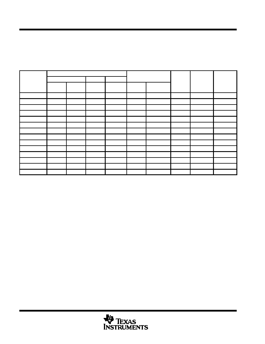
Table 1 provides a comparison of the devices in the 'C5x generation. It shows the capacity of on-chip RAM and
ROM memories, number of serial and parallel I/O ports, execution time of one machine cycle, and type of
package with total pin count.
Table 1. Characteristics of the 'C5x Processors
ON-CHIP MEMORY (16-BIT WORDS)
I/O PORTS
POWER
CYCLE
TMS320
DARAM
SARAM
ROM
I/O PORTS
POWER
SUPPLY
CYCLE
TIME
PACKAGE
TYPE
DEVICES
DATA
DATA +
PROG
DATA +
PROG
PROG
SERIAL
PARALLEL
SUPPLY
(V)
TIME
(ns)
TYPE
QFP
TMS320C50
544
512
9K
2Kß
2
64K
5
50/35/25
132 pin
TMS320LC50
544
512
9K
2Kß
2
64K
3.3
50/40/25
132 pin
TMS320C51
544
512
1K
8Kß
2
64K
5
50/35/25/20
100/132 pin
TMS320LC51
544
512
1K
8Kß
2
64K
3.3
50/40/25
100/132 pin
TMS320C52
544
512
≠
4Kß
1∂
64K
5
50/35/25/20
100 pin
TMS320LC52
544
512
≠
4Kß
1∂
64K
3.3
50/40/25
100 pin
TMS320C53
544
512
3K
16Kß
2
64K
5
50/35/25
132 pin
TMS320LC53
544
512
3K
16Kß
2
64K
3.3
50/40/25
132 pin
TMS320C53S
544
512
3K
16Kß
2 ∂
64K
5
50/35/25
100 pin
TMS320LC53S
544
512
3K
16Kß
2 ∂
64K
3.3
50/40/25
100 pin
TMS320LC56
544
512
6K
32K
2 #
64K
3.3
35/25
100 pin
TMS320LC57
544
512
6K
32K
2 #
64K + HPI ||
3.3
35/25
128 pin
TMS320C57S
544
512
6K
2Kß
2 #
64K + HPI ||
5
50/35/25
144 pin
TMS320LC57S
544
512
6K
2Kß
2 #
64K + HPI ||
3.3
50/35
144 pin
Sixteen of the 64K parallel I/O ports are memory mapped.
QFP = Quad flatpack
ß ROM boot loader available
∂ TDM serial port not available
# Includes auto-buffered serial port (BSP) but TDM serial port not available
|| HPI = Host port interface
Pinouts for each package are device-specific.
TMS320C5x, TMS320LC5x
DIGITAL SIGNAL PROCESSORS
SPRS030A ≠ APRIL 1995 ≠ REVISED APRIL 1996
3
POST OFFICE BOX 1443
∑
HOUSTON, TEXAS 77251≠1443
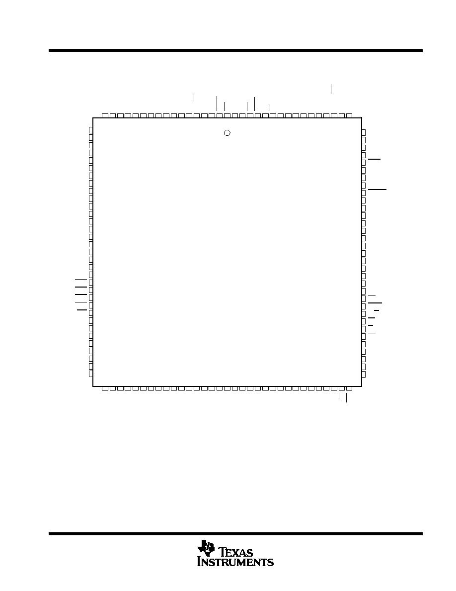
TMS320C50, TMS320LC50, TMS320C51, TMS320LC51, TMS320C53, TMS320LC53
PQ PACKAGE
( TOP VIEW )
WE
DDA
V
DDA
V
VSSD
VSSD
D7
D6
D5
D4
D3
D2
D1
D0
TMS
VDDD
VDDD
TCK
VSSD
VSSD
INT1
INT2
INT3
INT4
NMI
DR
TDR
FSR
CLKR
VDDA
VDDA
VSSC
VSSC
DS
IS
PS
R/ W
STRB
BR
CLKIN2
X2 / CLKIN
X1
VDDC
VDDC
TDO
VSSI
VSSI
FSX
TFSX / TFRM
DX
TDX
HOLDA
XF
CLKOUT1
NC
IACK
VDDI
VDDI
17 16 15 14 13 12 11 10
9
8
7
6
5
4
3
2
1 132 131 130 129 128 127 126 125 124 123 122 121 120 119 118 117
116
115
114
113
112
111
110
109
108
107
106
105
104
103
102
101
100
99
98
97
96
95
94
93
92
91
90
89
88
87
86
85
84
36
50
49
48
47
46
45
44
43
42
41
40
39
38
37
35
34
33
32
31
30
29
28
27
26
25
24
23
22
21
20
19
18
DDD
V
DDD
V
D8
D9
D10
D1
1
D12
D13
D14
D15
MP/
MC
TRST
IAQ
SSI
V
SSI
V
51 52 53 54 55 56 57 58 59 60 61 62 63 64 65 66 67 68 69 70 71 72 73 74 75 76 77 78
80 81 82 83
DDC
V
DDC
V
BIO
HOLD
READY
RS
TCLKR
TFSR
/
T
ADD
CLKX
TCLKX
T
OUT
EMU1/
OFF
EMU0
SSC
V
SSC
V
SSA
V
SSA
V
A0
A1
A2
A3
A4
A5
A6
A7
A8
TDI
A9
CLKMD1
A10
A1
1
A12
A13
A14
A15
DDI
V
DDI
V
SSA
V
SSA
V
RD
79
NC
NC
NC
NC
NC
NC
NC
NC
NC
NC
NC
NC
NC
NC
NC
NC
CLKMD2
NC
NC
NC
NOTE: NC = No connect (These pins are reserved.)

TMS320C5x, TMS320LC5x
DIGITAL SIGNAL PROCESSORS
SPRS030A ≠ APRIL 1995 ≠ REVISED APRIL 1996
4
POST OFFICE BOX 1443
∑
HOUSTON, TEXAS 77251≠1443
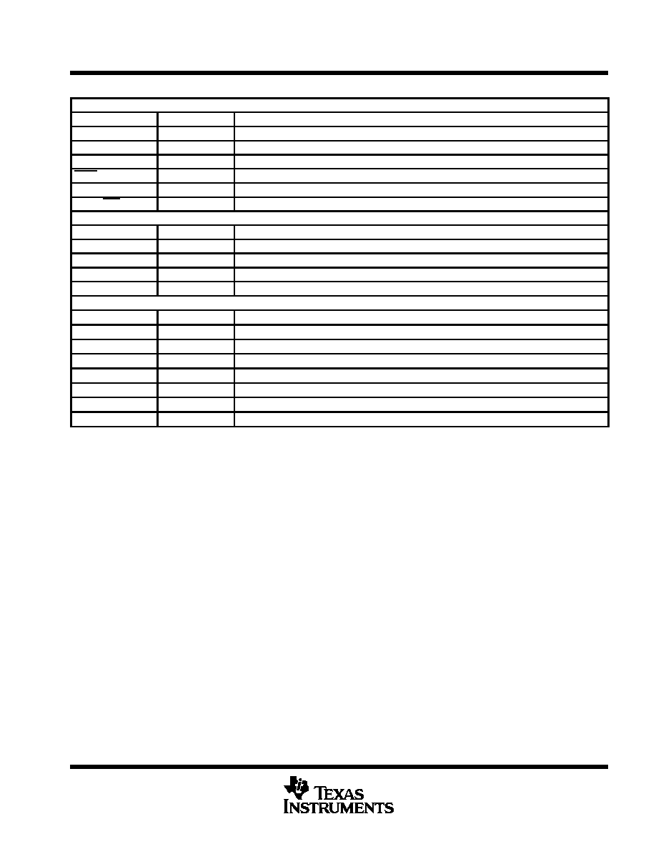
Pin Functions for Devices in the PQ Package
SIGNAL
TYPE
DESCRIPTION
PARALLEL INTERFACE BUS
A0 ≠ A15
I / O / Z
16-bit external address bus (MSB: A15, LSB: A0)
D0 ≠ D15
I / O / Z
16-bit external data bus (MSB: D15, LSB: D0)
PS, DS, IS
O / Z
Program, data, and I /O space select outputs, respectively
STRB
I / O / Z
Timing strobe for external cycles and external DMA
R / W
I / O / Z
Read / write select for external cycles and external DMA
RD, WE
O / Z
Read and write strobes, respectively, for external cycles
READY
I
External bus ready/ wait-state control input
BR
I / O / Z
Bus request. Arbitrates global memory and external DMA
SYSTEM INTERFACE / CONTROL SIGNALS
RS
I
Reset. Initializes device and sets PC to zero
MP/ MC
I
Microprocessor/microcomputer mode select. Enables internal ROM
HOLD
I
Puts parallel I/ F bus in high-impedance state after current cycle
HOLDA
O / Z
Hold acknowledge. Indicates external bus in hold state
XF
O / Z
External flag output. Set /cleared through software
BIO
I
I /O branch input. Implements conditional branches
TOUT
O / Z
Timer output signal. Indicates output of internal timer
IAQ
O / Z
Instruction acquisition signal
IACK
O / Z
Interrupt acknowledge signal
INT1 ≠ INT4
I
External interrupt inputs
NMI
I
Nonmaskable external interrupt
SERIAL PORT INTERFACE (SPI)
DR
I
Serial receive-data input
DX
O / Z
Serial transmit-data output. In high-impedance state when not transmitting
CLKR
I
Serial receive-data clock input
CLKX
I / O / Z
Serial transmit-data clock. Internal or external source
FSR
I
Serial receive-frame-synchronization input
FSX
I / O / Z
Serial transmit-frame-synchronization signal. Internal or external source
TDM SERIAL-PORT INTERFACE
TDR
I
TDM serial receive-data input
TDX
O / Z
TDM serial transmit-data output. In high-impedance state when not transmitting
TCLKR
I
TDM serial receive-data clock input
TCLKX
I / O / Z
TDM serial transmit-data clock. Internal or external source
TFSR / TADD
I / O / Z
TDM serial receive-frame-synchronization input. In the TDM mode, TFSR / TADD is used to output /
input the address of the port.
TFSX / TFRM
I
TDM serial transmit-frame-synchronization signal. Internal or external source. In the TDM mode,
TFSX / TFRM becomes TFRM, the TDM frame synchronization.
LEGEND:
I = Input
O = Output
Z = High impedance
TMS320C5x, TMS320LC5x
DIGITAL SIGNAL PROCESSORS
SPRS030A ≠ APRIL 1995 ≠ REVISED APRIL 1996
5
POST OFFICE BOX 1443
∑
HOUSTON, TEXAS 77251≠1443
Pin Functions for Devices in the PQ Package (Continued)
EMULATION/IEEE STANDARD 1149.1 TEST ACCESS PORT (TAP)
TDI
I
TAP scan data input
TDO
O / Z
TAP scan data output
TMS
I
TAP mode select input
TCK
I
TAP clock input
TRST
I
TAP reset (with pulldown resistor). Disables TAP when low
EMU0
I / O / Z
Emulation control 0. Reserved for emulation use
EMU1 / OFF
I / O / Z
Emulation control 1. Puts outputs in high-impedance state when low
CLOCK GENERATION AND CONTROL
X1
O
Oscillator output
X2 / CLKIN
I
Clock/oscillator input
CLKIN2
I
Clock input
CLKMD1, CLKMD2
I
Clock-mode select inputs
CLKOUT1
O / Z
Device system-clock output
POWER SUPPLY CONNECTIONS
VDDA
S
Supply connection, address-bus output
VDDD
S
Supply connection, data-bus output
VDDC
S
Supply connection, control output
VDDI
S
Supply connection, internal logic
VSSA
S
Supply connection, address-bus output
VSSD
S
Supply connection, data-bus output
VSSC
S
Supply connection, control output
VSSI
S
Supply connection, internal logic
LEGEND:
I = Input
O = Output
S = Supply
Z = High impedance