
TMS320C54x, TMS320LC54x, TMS320VC54x
FIXED-POINT DIGITAL SIGNAL PROCESSORS
SPRS039C ≠ FEBRUARY 1996 ≠ REVISED DECEMBER 1999
1
POST OFFICE BOX 1443
∑
HOUSTON, TEXAS 77251≠1443
D
Advanced Multibus Architecture With Three
Separate 16-Bit Data Memory Buses and
One Program Memory Bus
D
40-Bit Arithmetic Logic Unit (ALU)
Including a 40-Bit Barrel Shifter and Two
Independent 40-Bit Accumulators
D
17-
◊
17-Bit Parallel Multiplier Coupled to a
40-Bit Dedicated Adder for Non-Pipelined
Single-Cycle Multiply/Accumulate (MAC)
Operation
D
Compare, Select, and Store Unit (CSSU) for
the Add/Compare Selection of the Viterbi
Operator
D
Exponent Encoder to Compute an
Exponent Value of a 40-Bit Accumulator
Value in a Single Cycle
D
Two Address Generators With Eight
Auxiliary Registers and Two Auxiliary
Register Arithmetic Units (ARAUs)
D
Data Bus With a Bus Holder Feature
D
Address Bus With a Bus Holder Feature
('548 and '549 Only)
D
Extended Addressing Mode for 8M
◊
16-Bit
Maximum Addressable External Program
Space ('548 and '549 Only)
D
192K
◊
16-Bit Maximum Addressable
Memory Space (64K Words Program,
64K Words Data, and 64K Words I/O)
D
On-Chip ROM with Some Configurable to
Program/Data Memory
D
Dual-Access On-Chip RAM
D
Single-Access On-Chip RAM ('548/'549)
D
Single-Instruction Repeat and
Block-Repeat Operations for Program Code
D
Block-Memory-Move Instructions for Better
Program and Data Management
D
Instructions With a 32-Bit Long Word
Operand
D
Instructions With Two- or Three-Operand
Reads
D
Arithmetic Instructions With Parallel Store
and Parallel Load
D
Conditional Store Instructions
D
Fast Return From Interrupt
D
On-Chip Peripherals
≠ Software-Programmable Wait-State
Generator and Programmable Bank
Switching
≠ On-Chip Phase-Locked Loop (PLL) Clock
Generator With Internal Oscillator or
External Clock Source
≠ Full-Duplex Serial Port to Support 8- or
16-Bit Transfers ('541, 'LC545, and
'LC546 Only)
≠ Time-Division Multiplexed (TDM) Serial
Port ('542, '543, '548, and '549 Only)
≠ Buffered Serial Port (BSP) ('542, '543,
'LC545, 'LC546, '548, and '549 Only)
≠ 8-Bit Parallel Host-Port Interface (HPI)
('542, 'LC545, '548, and '549)
≠ One 16-Bit Timer
≠ External-Input/Output (XIO) Off Control
to Disable the External Data Bus,
Address Bus and Control Signals
D
Power Consumption Control With IDLE1,
IDLE2, and IDLE3 Instructions With
Power-Down Modes
D
CLKOUT Off Control to Disable CLKOUT
D
On-Chip Scan-Based Emulation Logic,
IEEE Std 1149.1
(JTAG) Boundary Scan
Logic
D
25-ns Single-Cycle Fixed-Point Instruction
Execution Time [40 MIPS] for 5-V Power
Supply ('C541 and 'C542 Only)
D
20-ns and 25-ns Single-Cycle Fixed-Point
Instruction Execution Time (50 MIPS and
40 MIPS) for 3.3-V Power Supply ('LC54x)
D
15-ns Single-Cycle Fixed-Point Instruction
Execution Time (66 MIPS) for 3.3-V Power
Supply ('LC54xA, '548, 'LC549)
D
12.5-ns Single-Cycle Fixed-Point
Instruction Execution Time (80 MIPS) for
3.3-V Power Supply ('LC548, 'LC549)
D
10-ns and 8.3-ns Single-Cycle Fixed-Point
Instruction Execution Time (100 and 120
MIPS) for 3.3-V Power Supply (2.5-V Core)
('VC549)
Please be aware that an important notice concerning availability, standard warranty, and use in critical applications of
Texas Instruments semiconductor products and disclaimers thereto appears at the end of this data sheet.
Copyright
©
1999, Texas Instruments Incorporated
IEEE Standard 1149.1-1990 Standard-Test-Access Port and Boundary Scan Architecture.
PRODUCTION DATA information is current as of publication date.
Products conform to specifications per the terms of Texas Instruments
standard warranty. Production processing does not necessarily include
testing of all parameters.

TMS320C54x, TMS320LC54x, TMS320VC54x
FIXED-POINT DIGITAL SIGNAL PROCESSORS
SPRS039C ≠ FEBRUARY 1996 ≠ REVISED DECEMBER 1999
2
POST OFFICE BOX 1443
∑
HOUSTON, TEXAS 77251≠1443
description
The TMS320C54x, TMS320LC54x, and TMS320VC54x fixed-point, digital signal processor (DSP) families
(hereafter referred to as the '54x unless otherwise specified) are based on an advanced modified Harvard
architecture that has one program memory bus and three data memory buses. These processors also provide
an arithmetic logic unit (ALU) that has a high degree of parallelism, application-specific hardware logic, on-chip
memory, and additional on-chip peripherals. These DSP families also provide a highly specialized instruction
set, which is the basis of the operational flexibility and speed of these DSPs.
Separate program and data spaces allow simultaneous access to program instructions and data, providing the
high degree of parallelism. Two reads and one write operation can be performed in a single cycle. Instructions
with parallel store and application-specific instructions can fully utilize this architecture. In addition, data can be
transferred between data and program spaces. Such parallelism supports a powerful set of arithmetic, logic,
and bit-manipulation operations that can all be performed in a single machine cycle. In addition, the 'C54x,
'LC54x, and 'VC54x versions include the control mechanisms to manage interrupts, repeated operations, and
function calls.
Table 1 provides an overview of the '54x generation of DSPs. The table shows significant features of each
device including the capacity of on-chip RAM and ROM memories, the peripherals, the execution time of one
machine cycle, and the type of package with its total pin count.
Table 1. Characteristics of the '54x Processors
DSP TYPE
NOMINAL
ON-CHIP
MEMORY
PERIPHERALS
CYCLE
PACKAGE TYPE
DSP TYPE
NOMINAL
VOLTAGE (V)
RAM
(Word)
ROM
(Word)
SERIAL
PORT
TIMER
HPI
CYCLE
TIME (ns)
PACKAGE TYPE
TMS320C541
5.0
5K
28K
2ß
1
No
25
100-pin TQFP
TMS320LC541
3.3
5K
28K
2ß
1
No
20/25
100-pin TQFP
TMS320LC541B
h
3.3
5K
28K
2ß
1
No
20/25
100-pin TQFP
TMS320C542
5.0
10K
2K
2∂
1
Yes
25
144-pin TQFP
TMS320LC542
3.3
10K
2K
2∂
1
Yes
20/25
128-pin TQFP/144-pin TQFP
TMS320LC543
3.3
10K
2K
2∂
1
No
20/25
100-pin TQFP
TMS320LC545
3.3
6K
48K#
2||
1
Yes
20/25
128-pin TQFP
TMS320LC545A
h
3.3
6K
48K#
2||
1
Yes
15/20/25
128-pin TQFP
TMS320LC545B
h
3.3
6K
48K#
2||
1
Yes
15/20/25
128-pin TQFP
TMS320LC546
3.3
6K
48K#
2||
1
No
20/25
100-pin TQFP
TMS320LC546A
h
3.3
6K
48K#
2||
1
No
15/20/25
100-pin TQFP
TMS320LC546B
h
3.3
6K
48K#
2||
1
No
15/20/25
100-pin TQFP
TMS320LC548
h
3.3
32K
2K
3
k
1
Yes
12.5/15/20
144-pin TQFP/144-pin BGA
TMS320LC549
h
3.3
32K
16K
3
k
1
Yes
12.5/15
144-pin TQFP/144-pin BGA
TMS320VC549
h
3.3 (2.5 core)
32K
16K
3
k
1
Yes
8.3/10/12.5
144-pin TQFP/144-pin BGA
Legend:
TQFP = Thin Quad Flatpack
BGA = MicroStar BGA
TM
(Ball Grid Array)
The dual-access RAM (single access RAM on '548 and '549 devices) can be configured as data memory or program/data memory.
For 'C541/'LC541, 8K words of ROM can be configured as program memory or program/data memory.
ß Two standard (general-purpose) serial ports
∂ One TDM and one BSP
# For 'LC545/'LC546, 16K words of ROM can be configured as program memory or program/data memory.
|| One standard and one BSP
k
One TDM and two BSPs
h
Refer to separate data sheet for electrical specifications.
MicroStar BGA is a trademark of Texas Instruments Incorporated.

TMS320C54x, TMS320LC54x, TMS320VC54x
FIXED-POINT DIGITAL SIGNAL PROCESSORS
SPRS039C ≠ FEBRUARY 1996 ≠ REVISED DECEMBER 1999
3
POST OFFICE BOX 1443
∑
HOUSTON, TEXAS 77251≠1443
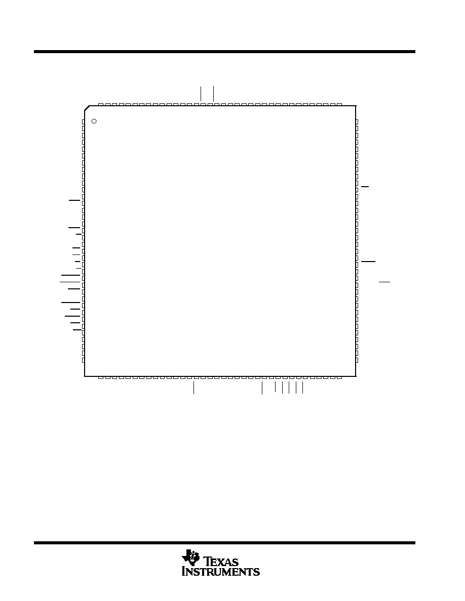
CLKR0
VSS
A10
A11
A12
A13
A14
A15
CVDD
VSS
CVDD
READY
PS
DS
IS
R/W
MSTRB
IOSTRB
MSC
XF
HOLDA
HOLD
BIO
MP/MC
1
2
3
4
5
6
7
8
9
10
11
12
13
14
15
16
17
18
19
20
21
22
23
24
25
76
77
78
79
80
81
82
83
84
85
86
87
88
89
90
91
92
93
94
95
96
97
98
99
100
75
74
73
72
71
70
69
68
67
66
65
64
63
62
61
60
59
58
57
56
55
54
53
52
51
50
49
48
47
46
45
44
43
42
41
40
39
38
37
36
35
34
33
32
31
30
29
28
27
26
A5
A4
A3
A2
A1
V
V
D14
D13
D12
D1
1
D10
D9
D8
D7
D6
DV
SS
CLKR1
FSR0
FSR1
DR0
DR1
CLKX1
DD
FSX1
DD
SS
INT1
INT3
SS
VSS
A6
D15
INT2
TMS320C541, TMS320LC541
PZ PACKAGE
(TOP VIEW)
IAQ
A0
CLKX0
NMI
D5
D4
D3
D2
D1
D0
RS
X2/CLKIN
X1
VSS
CVDD
VSS
TMS
TCK
TRST
TDI
TDO
EMU1/OFF
EMU0
TOUT
CLKMD3
CLKMD2
CLKMD1
CLKOUT
CNT
A9
A8
A7
SS
SS
DD
V
DV
V
V
CV
SS
V
FSX0
DX0
DX1
IACK
DD
CV
INT0
CV
DD
DV
DD
DVDD is the power supply for the I/O pins while CVDD is the power supply for the core CPU, and VSS is the ground for both the I/O pins and the
core CPU.
The '54x signal descriptions table lists each terminal name, function, and operating mode(s) for the
TMS320C541PZ/TMS320LC541PZ (100-pin TQFP packages).
For the 'C541/'LC541 (100-pin packages), no letter in front of CLKRn, FSRn, DRn, CLKXn, FSXn, and DXn pin
names denotes standard serial port (where n = 0 or 1 port).
TMS320C54x, TMS320LC54x, TMS320VC54x
FIXED-POINT DIGITAL SIGNAL PROCESSORS
SPRS039C ≠ FEBRUARY 1996 ≠ REVISED DECEMBER 1999
4
POST OFFICE BOX 1443
∑
HOUSTON, TEXAS 77251≠1443
CV
HDS1
VSS
NC
VSS
DVDD
D5
D4
D3
D2
D1
D0
RS
X2 / CLKIN
X1
HD3
CLKOUT
VSS
HPIENA
CVDD
VSS
TMS
TCK
TRST
TDI
TDO
EMU1 / OFF
EMU0
TOUT
HD2
CNT
CLKMD3
CLKMD2
CLKMD1
VSS
DVDD
NC
VSS
VSS
NC
VSS
DVDD
A10
HD7
A11
A12
A13
A14
A15
CVDD
HAS
VSS
VSS
CVDD
HCS
HR / W
READY
PS
DS
IS
R / W
MSTRB
IOSTRB
MSC
XF
HOLDA
IAQ
HOLD
BIO
MP / MC
DVDD
VSS
NC
VSS
SS
V
144
NC
CV
143
142
141
A8
140
A7
139
A6
138
A5
137
A4
136
HD6
135
A3
134
A2
133
A1
132
A0
131
DV
130
129
128
127
V
126
125
HD5
124
D15
123
D14
122
D13
121
HD4
120
D12
11
9
D1
1
11
8
11
7
D9
11
6
D8
11
5
D7
11
4
D6
11
3
11
2
37
38
39
40
41
42
43
44
45
46
47
48
49
50
51
52
53
54
55
56
57
58
59
60
61
62
63
64
65
66
67
68
69
1
2
3
4
5
6
7
8
9
10
11
12
13
14
15
16
17
18
19
20
21
22
23
24
25
26
27
28
29
30
31
32
33
34
35
36
108
107
106
105
104
103
102
101
100
99
98
97
96
95
94
93
92
91
90
89
88
87
86
85
84
83
82
81
80
79
78
77
76
75
74
73
SS
V
NC
HCNTL0
SS
BCLKR
TCLKR
BFSR
TFSR
/
T
ADD
BDR
HCNTL1
TDR
BCLKX
TCLKX
SS
DD
SS
HD0
BDX
TDX
IACK
HBIL
NMI
INT0
INT1
INT2
INT3
DD
HD1
SS
HRDY
HINT
111
V
11
0
V
109
70
71
72
NC
SS
V
D10
TFSX
/
TFRM
SS
NC
DV
DD
CV
HDS2
SS
V
V
V
DV
V
CV
V
DD
DD
DD
DD
SS
SS
TMS320C542/TMS320LC542
PGE PACKAGE
(TOP VIEW)
BFSX
A9
NC = No connection
DVDD is the power supply for the I/O pins while CVDD is the power supply for the core CPU, and VSS is the ground for both the I/O pins and the
core CPU.
The '54x signal descriptions table lists each terminal name, function, and operating mode(s) for the
TMS320C542PGE/'LC542PGE (144-pin TQFP packages).
For the 'C542/'LC542 (144-pin TQFP packages), the letter B in front of CLKR, FSR, DR, CLKX, FSX, and DX
pin names denotes buffered serial port (BSP). The letter T in front of CLKR, FSR, DR, CLKX, FSX, and DX pin
names denotes time-division multiplexed (TDM) serial port.

TMS320C54x, TMS320LC54x, TMS320VC54x
FIXED-POINT DIGITAL SIGNAL PROCESSORS
SPRS039C ≠ FEBRUARY 1996 ≠ REVISED DECEMBER 1999
5
POST OFFICE BOX 1443
∑
HOUSTON, TEXAS 77251≠1443
VSS
DVDD
A10
HD7
A11
A12
A13
A14
A15
CVDD
HAS
VSS
VSS
CVDD
HCS
HR / W
READY
PS
DS
IS
R / W
MSTRB
IOSTRB
MSC
XF
HOLDA
IAQ
HOLD
BIO
MP / MC
DVDD
VSS
VSS
DVDD
D5
D4
D3
D2
D1
D0
RS
X2 / CLKIN
X1
HD3
CLKOUT
VSS
HPIENA
CVDD
VSS
TMS
TCK
TRST
TDI
TDO
EMU1 / OFF
EMU0
TOUT
HD2
CNT
CLKMD3
CLKMD2
CLKMD1
VSS
DVDD
96
95
94
93
92
91
90
89
88
87
86
85
84
83
82
81
80
79
78
77
76
75
74
73
72
71
70
69
68
67
66
65
1
2
3
4
5
6
7
8
9
10
11
12
13
14
15
16
17
18
19
20
21
22
23
24
25
26
27
28
29
30
31
32
128
33
127 126 125 124 123 122 121 120 119 118 117 116 115 114 113 112 111 110 109 108 107 106 105 104 103 102 101 100 99 98 97
34 35 36 37 38 39 40 41 42 43 44 45 46 47 48 49 50 51 52 53 54 55 56 57 58 59 60 61 62 63 64
HCNTL0
CV
SS
A9
BCLKR
A8
TCLKR
A7
BFSR
A6
TFSR
/
T
ADD
A5
BDR
A4
HCNTL1
HD6
TDR
A3
BCLKX
A2
TCLKX
A1
SS
A0
HINT
DV
DD
HDS2
BFSX
V
TFSX
/
TFRM
HDS1
HRDY
V
DD
CV
SS
HD5
HD0
D15
BDX
D14
TDX
D13
IACK
HD4
HBIL
D12
NMI
D1
1
INT0
D10
INT1
D9
INT2
D8
INT3
D7
DD
D6
HD1
DV
SS
V
DD
DD
V
CV
V
CV
DV
V
V
SS
DD
DD
SS
TMS320LC542
PBK PACKAGE
( TOP VIEW )
SS
DVDD is the power supply for the I/O pins while CVDD is the power supply for the core CPU, and VSS is the ground for both the I/O pins and the
core CPU.
The '54x signal descriptions table lists each terminal name, function, and operating mode(s) for the
TMS320LC542PBK (128-pin TQFP package).
For the 'LC542 (128-pin TQFP package), the letter B in front of CLKR, FSR, DR, CLKX, FSX, and DX pin names
denotes buffered serial port (BSP). The letter T in front of CLKR, FSR, DR, CLKX, FSX, and DX pin names
denotes time-division multiplexed (TDM) serial port.