 | –≠–Ľ–Ķ–ļ—ā—Ä–ĺ–Ĺ–Ĺ—č–Ļ –ļ–ĺ–ľ–Ņ–ĺ–Ĺ–Ķ–Ĺ—ā: TLV1549C | –°–ļ–į—á–į—ā—Ć:  PDF PDF  ZIP ZIP |
TLV1549C, TLV1549I, TLV1549M
10-BIT ANALOG-TO-DIGITAL CONVERTERS
WITH SERIAL CONTROL
SLAS071C ≠ JANUARY 1993 ≠ REVISED MARCH 1995
1
POST OFFICE BOX 655303
∑
DALLAS, TEXAS 75265
D
3.3-V Supply Operation
D
10-Bit-Resolution Analog-to-Digital
Converter (ADC)
D
Inherent Sample and Hold Function
D
Total Unadjusted Error . . .
Ī
1 LSB Max
D
On-Chip System Clock
D
Terminal Compatible With TLC1549 and
TLC1549x
D
Application Report Available
D
CMOS Technology
description
The TLV1549C, TLV1549I, and TLV1549M are
10-bit, switched-capacitor, successive-
approximation, analog-to-digital converters. The
devices have two digital inputs and a 3-state
output [chip select (CS), input-output clock (I/O
CLOCK), and data output (DATA OUT)] that
provide a three-wire interface to the serial port of
a host processor.
The sample-and-hold function is automatic. The
converter incorporated in the device features
differential high-impedance reference inputs that
facilitate ratiometric conversion, scaling, and
isolation of analog circuitry from logic and supply
noise. A switched-capacitor design allows low-
error conversion over the full operating free-air
temperature range.
The TLV1549C is characterized for operation from 0
į
C to 70
į
C. The TLV1549I is characterized for operation
from ≠ 40
į
C to 85
į
C. The TLV1549M is characterized for operation over the full military temperature range of
≠ 55
į
C to 125
į
C.
AVAILABLE OPTIONS
PACKAGE
TA
SMALL OUTLINE
(D)
CHIP CARRIER
(FK)
CERAMIC DIP
(JG)
PLASTIC DIP
(P)
0
į
C to 70
į
C
TLV1549CD
--
--
TLV1549CP
≠ 40
į
C to 85
į
C
TLV1549ID
--
--
TLV1549IP
≠ 55
į
C to 125
į
C
--
TLV1549MFK
TLV1549MJG
--
Interfacing the TLV1549 10-Bit Serial-Out ADC to Popular 3.3-V Microcontrollers (SLAA005)
Copyright
©
1995, Texas Instruments Incorporated
PRODUCTION DATA information is current as of publication date.
Products conform to specifications per the terms of Texas Instruments
standard warranty. Production processing does not necessarily include
testing of all parameters.
Please be aware that an important notice concerning availability, standard warranty, and use in critical applications of
Texas Instruments semiconductor products and disclaimers thereto appears at the end of this data sheet.
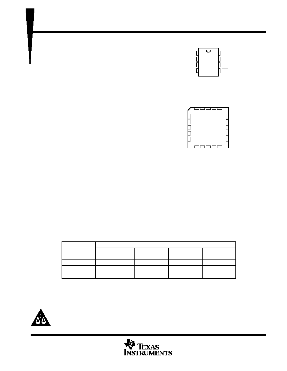
1
2
3
4
8
7
6
5
REF +
ANALOG IN
REF ≠
GND
V
CC
I/O CLOCK
DATA OUT
CS
D, JG, OR P PACKAGE
(TOP VIEW)
3
2
1 20 19
9 10 11 12 13
4
5
6
7
8
18
17
16
15
14
NC
I/O CLOCK
NC
DATA OUT
NC
NC
ANALOG IN
NC
REF≠
NC
FK PACKAGE
(TOP VIEW)
NC
REF+
NC
CS
NC
NC
NC
GND
NC
NC ≠ No internal connection
CC
V
TLV1549C, TLV1549I, TLV1549M
10-BIT ANALOG-TO-DIGITAL CONVERTERS
WITH SERIAL CONTROL
SLAS071C ≠ JANUARY 1993 ≠ REVISED MARCH 1995
2
POST OFFICE BOX 655303
∑
DALLAS, TEXAS 75265
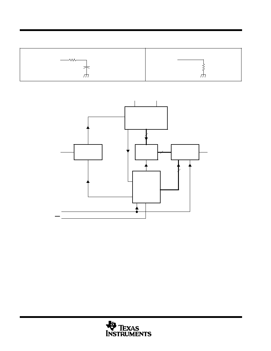
typical equivalent inputs
INPUT CIRCUIT IMPEDANCE DURING SAMPLING MODE
INPUT CIRCUIT IMPEDANCE DURING HOLD MODE
1 k
TYP
Ci = 60 pF TYP
(equivalent input
capacitance)
5 M
TYP
ANALOG IN
ANALOG IN
functional block diagram
Sample and
Hold
10-Bit
Analog-to-Digital
Converter
(switched capacitors)
Output
Data
Register
10-to-1 Data
Selector and
Driver
System Clock,
Control Logic,
and I/O
Counters
10
10
4
REF +
REF ≠
DATA OUT
ANALOG IN
3
1
6
7
5
I/O CLOCK
CS
2
Terminal numbers shown are for the D, JG, and P packages only.
TLV1549C, TLV1549I, TLV1549M
10-BIT ANALOG-TO-DIGITAL CONVERTERS
WITH SERIAL CONTROL
SLAS071C ≠ JANUARY 1993 ≠ REVISED MARCH 1995
3
POST OFFICE BOX 655303
∑
DALLAS, TEXAS 75265
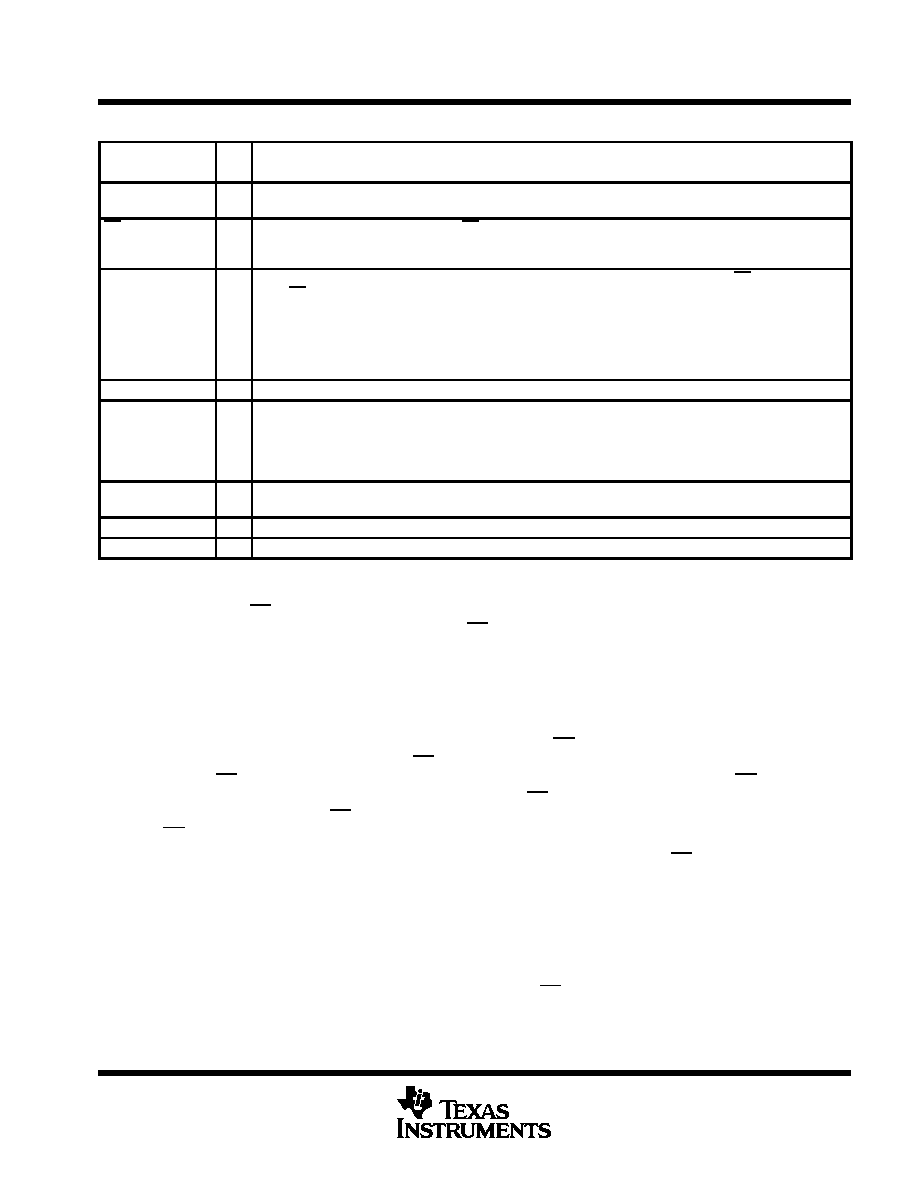
Terminal Functions
TERMINAL
I/O
DESCRIPTION
NAME
NO.
I/O
DESCRIPTION
ANALOG IN
2
I
Analog input. The driving source impedance should be
1 k
. The external driving source to ANALOG IN should
have a current capability
10 mA.
CS
5
I
Chip select. A high-to-low transition on CS resets the internal counters and controls and enables DATA OUT and
I/O CLOCK within a maximum of a setup time plus two falling edges of the internal system clock. A low-to-high
transition disables I/O CLOCK within a setup time plus two falling edges of the internal system clock.
DATA OUT
6
O
This 3-state serial output for the A/D conversion result is in the high-impedance state when CS is high and active
when CS is low. With a valid chip select, DATA OUT is removed from the high-impedance state and is driven to
the logic level corresponding to the MSB value of the previous conversion result. The next falling edge of I/O
CLOCK drives DATA OUT to the logic level corresponding to the next most significant bit, and the remaining bits
are shifted out in order with the LSB appearing on the ninth falling edge of I/O CLOCK. On the tenth falling edge
of I/O CLOCK, DATA OUT is driven to a low logic level so that serial interface data transfers of more than ten clocks
produce zeroes as the unused LSBs.
GND
4
I
The ground return for internal circuitry. Unless otherwise noted, all voltage measurements are with respect to GND.
I/O CLOCK
7
I
The input /output clock receives the serial I/O CLOCK input and performs the following three functions:
1) On the third falling edge of I/O CLOCK, the analog input voltage begins charging the capacitor array and
continues to do so until the tenth falling edge of I/O CLOCK.
2) It shifts the nine remaining bits of the previous conversion data out on DATA OUT.
3) It transfers control of the conversion to the internal state controller on the falling edge of the tenth clock.
REF +
1
I
The upper reference voltage value (nominally VCC) is applied to REF +. The maximum input voltage range is
determined by the difference between the voltage applied to REF + and the voltage applied to REF ≠.
REF ≠
3
I
The lower reference voltage value (nominally ground) is applied to this REF ≠.
VCC
8
I
Positive supply voltage
detailed description
With chip select (CS) inactive (high), the I/O CLOCK input is initially disabled and DATA OUT is in the high-
impedance state. When the serial interface takes CS active (low), the conversion sequence begins with the
enabling of I/O CLOCK and the removal of DATA OUT from the high-impedance state. The serial interface then
provides the I/O CLOCK sequence to I/O CLOCK and receives the previous conversion result from DATA OUT.
I/O CLOCK receives an input sequence that is between 10 and 16 clocks long from the host serial interface.
The first ten I/O clocks provide the control timing for sampling the analog input.
There are six basic serial interface timing modes that can be used with the TLV1549. These modes are
determined by the speed of I/O CLOCK and the operation of CS as shown in Table 1. These modes are:
(1) a fast mode with a 10-clock transfer and CS inactive (high) between transfers, (2) a fast mode with a 10-clock
transfer and CS active (low) continuously, (3) a fast mode with an 11- to 16-clock transfer and CS inactive (high)
between transfers, (4) a fast mode with a 16-bit transfer and CS active (low) continuously, (5) a slow mode with
an 11- to 16-clock transfer and CS inactive (high) between transfers, and (6) a slow mode with a 16-clock transfer
and CS active (low) continuously.
The MSB of the previous conversion appears on DATA OUT on the falling edge of CS in mode 1, mode 3, and
mode 5, within 21
Ķ
s from the falling edge of the tenth I/O CLOCK in mode 2 and mode 4, and following the
16th clock falling edge in mode 6. The remaining nine bits are shifted out on the next nine falling edges of the
I/O CLOCK. Ten bits of data are transmitted to the host serial interface through DATA OUT. The number of serial
clock pulses used also depends on the mode of operation, but a minimum of ten clock pulses is required for
conversion to begin. On the tenth clock falling edge, the internal logic takes DATA OUT low to ensure that the
remaining bit values are zero if the I/O CLOCK transfer is more than ten clocks long.
Table 1 lists the operational modes with respect to the state of CS, the number of I/O serial transfer clocks that
can be used, and the timing on which the MSB of the previous conversion appears at the output.

TLV1549C, TLV1549I, TLV1549M
10-BIT ANALOG-TO-DIGITAL CONVERTERS
WITH SERIAL CONTROL
SLAS071C ≠ JANUARY 1993 ≠ REVISED MARCH 1995
4
POST OFFICE BOX 655303
∑
DALLAS, TEXAS 75265
Table 1. Mode Operation
MODES
CS
NO. OF
I/O CLOCKS
MSB AT DATA OUT
TIMING
DIAGRAM
Mode 1
High between conversion cycles
10
CS falling edge
Figure 6
Fast Modes
Mode 2
Low continuously
10
Within 21
Ķ
s
Figure 7
Fast Modes
Mode 3
High between conversion cycles
11 to 16
CS falling edge
Figure 8
Mode 4
Low continuously
16
Within 21
Ķ
s
Figure 9
Slow Modes
Mode 5
High between conversion cycles
11 to 16
CS falling edge
Figure 10
Slow Modes
Mode 6
Low continuously
16
16th clock falling edge
Figure 11
This timing also initiates serial-interface communication.
No more than 16 clocks should be used.
All the modes require a minimum period of 21
Ķ
s after the falling edge of the tenth I/O CLOCK before a new
transfer sequence can begin. During a serial I/O CLOCK data transfer, CS must be active (low) so that the I/O
CLOCK input is enabled. When CS is toggled between data transfers (modes 1, 3, and 5), the transitions at CS
are recognized as valid only if the level is maintained for a minimum period of 1.425
Ķ
s after the transition. If
the transfer is more than ten I/O clocks (modes 3, 4, 5, and 6), the rising edge of the eleventh clock must occur
within 9.5
Ķ
s after the falling edge of the tenth I/O CLOCK; otherwise, the device could lose synchronization with
the host serial interface and CS has to be toggled to restore proper operation.
fast modes
The device is in a fast mode when the serial I/O CLOCK data transfer is completed within 21
Ķ
s from the falling
edge of the tenth I/O CLOCK. With a 10-clock serial transfer, the device can only run in a fast mode.
mode 1: fast mode, CS inactive (high) between transfers, 10-clock transfer
In this mode, CS is inactive (high) between serial I/O-CLOCK transfers and each transfer is ten clocks long. The
falling edge of CS begins the sequence by removing DATA OUT from the high-impedance state. The rising edge
of CS ends the sequence by returning DATA OUT to the high-impedance state within the specified delay time.
Also, the rising edge of CS disables I/O CLOCK within a setup time plus two falling edges of the internal system
clock.
mode 2: fast mode, CS active (low) continuously, 10-clock transfer
In this mode, CS is active (low) between serial I/O-CLOCK transfers and each transfer is ten clocks long. After
the initial conversion cycle, CS is held active (low) for subsequent conversions. Within 21
Ķ
s after the falling
edge of the tenth I/O CLOCK, the MSB of the previous conversion appears at DATA OUT.
mode 3: fast mode, CS inactive (high) between transfers, 11- to 16-clock transfer
In this mode, CS is inactive (high) between serial I/O-CLOCK transfers and each transfer can be 11 to 16 clocks
long. The falling edge of CS begins the sequence by removing DATA OUT from the high-impedance state. The
rising edge of CS ends the sequence by returning DATA OUT to the high-impedance state within the specified
delay time. Also, the rising edge of CS disables I/O CLOCK within a setup time plus two falling edges of the
internal system clock.
mode 4: fast mode, CS active (low) continuously, 16-clock transfer
In this mode, CS is active (low) between serial I/O-CLOCK transfers and each transfer must be exactly 16 clocks
long. After the initial conversion cycle, CS is held active (low) for subsequent conversions. Within 21
Ķ
s after
the falling edge of the tenth I/O CLOCK, the MSB of the previous conversion appears at DATA OUT.
slow modes
In a slow mode, the serial I/O CLOCK data transfer is completed after 21
Ķ
s from the falling edge of the tenth
I/O CLOCK.
TLV1549C, TLV1549I, TLV1549M
10-BIT ANALOG-TO-DIGITAL CONVERTERS
WITH SERIAL CONTROL
SLAS071C ≠ JANUARY 1993 ≠ REVISED MARCH 1995
5
POST OFFICE BOX 655303
∑
DALLAS, TEXAS 75265
mode 5: slow mode, CS inactive (high) between transfers, 11- to 16-clock transfer
In this mode, CS is inactive (high) between serial I/O-CLOCK transfers and each transfer can be 11 to 16 clocks
long. The falling edge of CS begins the sequence by removing DATA OUT from the high-impedance state. The
rising edge of CS ends the sequence by returning DATA OUT to the high-impedance state within the specified
delay time. Also, the rising edge of CS disables I/O CLOCK within a setup time plus two falling edges of the
internal system clock.
mode 6: slow mode, CS active (low) continuously, 16-clock transfer
In this mode, CS is active (low) between serial I/O-CLOCK transfers and each transfer must be exactly 16 clocks
long. After the initial conversion cycle, CS is held active (low) for subsequent conversions. The falling edge of
the sixteenth I/O CLOCK then begins each sequence by removing DATA OUT from the low state, allowing the
MSB of the previous conversion to appear immediately at DATA OUT. The device is then ready for the next
16-clock transfer initiated by the serial interface.
analog input sampling
Sampling of the analog input starts on the falling edge of the third I/O CLOCK, and sampling continues for seven
I/O CLOCK periods. The sample is held on the falling edge of the tenth I/O CLOCK.
converter and analog input
The CMOS threshold detector in the successive-approximation conversion system determines each bit by
examining the charge on a series of binary-weighted capacitors (see Figure 1). In the first phase of the
conversion process, the analog input is sampled by closing the S
C
switch and all S
T
switches simultaneously.
This action charges all the capacitors to the input voltage.
In the next phase of the conversion process, all S
T
and S
C
switches are opened and the threshold detector
begins identifying bits by identifying the charge (voltage) on each capacitor relative to the reference (REF ≠)
voltage. In the switching sequence, ten capacitors are examined separately until all ten bits are identified and
then the charge-convert sequence is repeated. In the first step of the conversion phase, the threshold detector
looks at the first capacitor (weight = 512). Node 512 of this capacitor is switched to the REF+ voltage, and the
equivalent nodes of all the other capacitors on the ladder are switched to REF ≠. If the voltage at the summing
node is greater than the trip point of the threshold detector (approximately one-half V
CC
), a bit 0 is placed in
the output register and the 512-weight capacitor is switched to REF ≠. If the voltage at the summing node is less
than the trip point of the threshold detector, a bit 1 is placed in the register and this 512-weight capacitor remains
connected to REF + through the remainder of the successive-approximation process. The process is repeated
for the 256-weight capacitor, the 128-weight capacitor, and so forth down the line until all bits are determined.
With each step of the successive-approximation process, the initial charge is redistributed among the
capacitors. The conversion process relies on charge redistribution to determine the bits from MSB to LSB.