TL5501
6-BIT ANALOG-TO-DIGITAL CONVERTER
SLAS026 ≠ OCTOBER 1989 ≠ REVISED APRIL 1990
1
POST OFFICE BOX 655303
∑
DALLAS, TEXAS 75265
D
6-Bit Resolution
D
Linearity Error . . .
±
0.8%
D
Maximum Conversion Rate . . . 30 MHz Typ
D
Analog Input Voltage Range
V
CC
to V
CC
≠
2 V
D
Analog Input Dynamic Range . . . 1 V
D
TTL Digital I/O Level
D
Low Power Consumption
200 mW Typ
D
5-V Single-Supply Operation
D
Interchangeable With Fujitsu MB40576
description
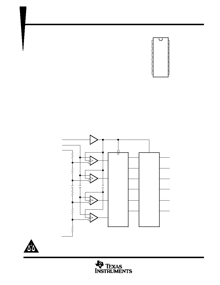
The TL5501 is a low-power ultra-high-speed video-band analog-to-digital converter that uses the Advanced
Low-Power Schottky (ALS) process. It utilizes the full-parallel comparison (flash method) for high-speed
conversion. It converts wide-band analog signals (such as a video signal) to a digital signal at a sampling rate
of dc to 30 MHz. Because of this high-speed capability, the TL5501 is suitable for digital video applications such
as digital TV, video processing with a computer, or radar signal processing.
The TL5501 is characterized for operation from 0
∞
C to 70
∞
C.
functional block diagram
D0 (LSB)
D1
D2
D3
D4
D5 (MSB)
EN
Latch
and
Buffer
63-to-6
Encoder
CLK
ANLG INPUT
REFT
REFB
63
62
2
1
R
R
R
R
R
Copyright
©
1990, Texas Instruments Incorporated
PRODUCTION DATA information is current as of publication date.
Products conform to specifications per the terms of Texas Instruments
standard warranty. Production processing does not necessarily include
testing of all parameters.
Please be aware that an important notice concerning availability, standard warranty, and use in critical applications of
Texas Instruments semiconductor products and disclaimers thereto appears at the end of this data sheet.
1
2
3
4
5
6
7
8
16
15
14
13
12
11
10
9
(LSB) D0
D1
D2
D3
D4
(MSB) D5
CLK
GND
GND
DGTL V
CC
ANLG V
CC
REFB
ANLG INPUT
REFT
ANLG V
CC
DGTL V
CC
N PACKAGE
(TOP VIEW)
TL5501
6-BIT ANALOG-TO-DIGITAL CONVERTER
SLAS026 ≠ OCTOBER 1989 ≠ REVISED APRIL 1990
2
POST OFFICE BOX 655303
∑
DALLAS, TEXAS 75265
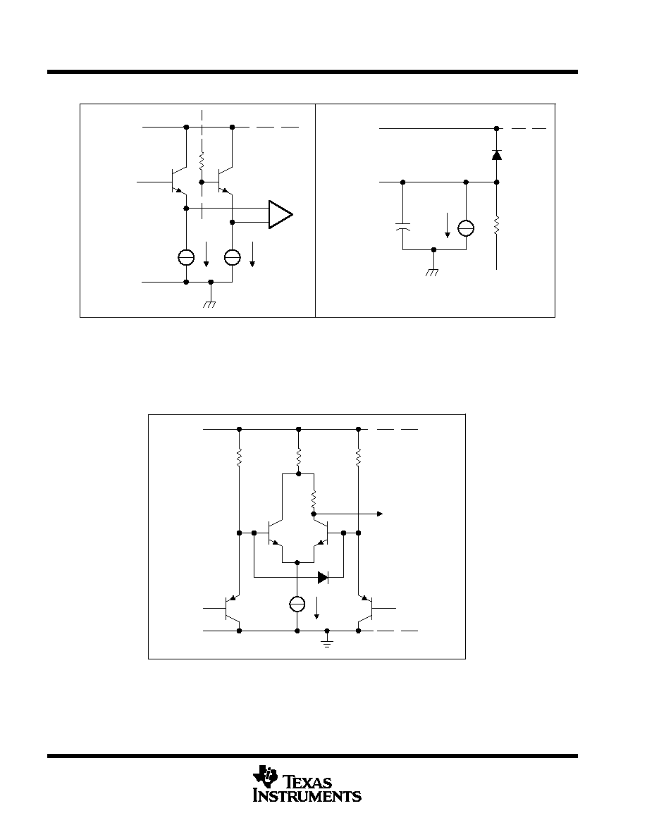
equivalents of analog input circuit
ANLG VCC
VI
D
ri
VrefB
(see Note A)
Ci
Ibias
ANLG GND
ANLG VCC
VI
NOTE A: Ci ≠ nonlinear emitter-follower junction capacitance
ri ≠ linear resistance model for input current transition caused by comparator switching.
VI < VrefB: Infinite; CLK high: infinite.
VrefB ≠ voltage at REFB terminal
Ibias ≠ constant input bias current
D ≠ base-collector junction diode of emitter-follower transistor
equivalent of digital input circuit
Vref = 1.4 V
Output
25 k
3.1 k
25 k
GND
VI
DGTL VCC
TL5501
6-BIT ANALOG-TO-DIGITAL CONVERTER
SLAS026 ≠ OCTOBER 1989 ≠ REVISED APRIL 1990
3
POST OFFICE BOX 655303
∑
DALLAS, TEXAS 75265
FUNCTION TABLE
STEP
ANALOG INPUT
VOLTAGE
DIGITAL OUTPUT CODE
0
3.992 V
L
L
L
L
L
L
1
4.008 V
L
L
L
L
L
H
|
|
|
31
4.488 V
L
H
H
H
H
H
32
4.508 V
H
L
L
L
L
L
33
4.520 V
H
L
L
L
L
H
|
|
|
62
4.984 V
H
H
H
H
H
L
63
5.000 V
H
H
H
H
H
H
These values are based on the assumption that VrefB and VrefT have been
adjusted so that the voltage at the transition from digital 0 to 1 (VZT) is
4.000 V and the transition to full scale (VFT) is 4.992 V. 1 LSB = 16 mV.
absolute maximum ratings over operating free-air temperature range (unless otherwise noted)
Supply voltage range, ANLG V
CC
(see Note 1)
≠ 0.5 V to 7 V
. . . . . . . . . . . . . . . . . . . . . . . . . . . . . . . . . . . . . . . .
Supply voltage range, DGTL V
CC
≠ 0.5 V to 7 V
. . . . . . . . . . . . . . . . . . . . . . . . . . . . . . . . . . . . . . . . . . . . . . . . . . . .
Input voltage range at digital input, V
I
≠ 0.5 V to 7 V
. . . . . . . . . . . . . . . . . . . . . . . . . . . . . . . . . . . . . . . . . . . . . . . . .
Input voltage range at analog input, V
I
≠ 0.5 V to ANLG V
CC
+ 0.5 V
. . . . . . . . . . . . . . . . . . . . . . . . . . . . . . . . . .
Analog reference voltage range, V
ref
≠ 0.5 V to ANLG V
CC
+ 0.5 V
. . . . . . . . . . . . . . . . . . . . . . . . . . . . . . . . . . .
Storage temperature range
≠ 55
∞
C to 150
∞
C
. . . . . . . . . . . . . . . . . . . . . . . . . . . . . . . . . . . . . . . . . . . . . . . . . . . . . . . .
Operating free-air temperature range
0
∞
C to 70
∞
C
. . . . . . . . . . . . . . . . . . . . . . . . . . . . . . . . . . . . . . . . . . . . . . . . . .
Lead temperature 1,6 mm (1/16 inch) from case for 10 seconds
260
∞
C
. . . . . . . . . . . . . . . . . . . . . . . . . . . . . . .
NOTE 1: All voltage values are with respect to the network ground terminal.
recommended operating conditions
MIN
NOM
MAX
UNIT
Supply voltage, ANLG VCC
4.75
5
5.25
V
Supply voltage, DGTL VCC
4.75
5
5.25
V
High-level input voltage, VIH
2
V
Low-level input voltage, VIL
0.8
V
Input voltage at analog input, VI (see Note 2)
4
5
V
Analog reference voltage (top side), VrefT (see Note 2)
4
5
5.1
V
Analog reference voltage (bottom side), VrefB (see Note 2)
3
4
4.1
V
High-level output current, IOH
≠ 400
µ
A
Low-level output current, IOL
4
mA
Clock pulse duration, high-level or low-level, tw
25
ns
Operating free-air temperature, TA
0
70
∞
C
NOTE 2: VrefB < VI < Vref T, Vref T ≠ VrefB = 1 V
±
0.1 V.
TL5501
6-BIT ANALOG-TO-DIGITAL CONVERTER
SLAS026 ≠ OCTOBER 1989 ≠ REVISED APRIL 1990
4
POST OFFICE BOX 655303
∑
DALLAS, TEXAS 75265
electrical characteristics over operating supply voltage range, T
A
= 25
∞
C (unless otherwise noted)
PARAMETER
TEST CONDITIONS
MIN
TYP
MAX
UNIT
II
Analog input current
VI = 5 V
75
µ
A
II
Analog input current
VI = 4 V
73
µ
A
IIH
Digital high-level input current
VI = 2.7 V
0
20
µ
A
IIL
Digital low-level input current
VI = 0.4 V
≠ 400
≠ 40
µ
A
II
Digital input current
VI = 7 V
100
µ
A
IrefB
Reference current
VIrefB = 4 V
≠ 4
≠ 7.2
mA
Iref T
Reference current
VIrefB = 5 V
4
7.2
mA
VOH
High-level output voltage
IOH = ≠ 400
µ
A
2.7
V
VOL
Low-level output voltage
IOL = 1.6 mA
0.4
V
ri
Analog input resistance
100
k
1Ci
Analog input capacitance
35
65
pF
ICC
Supply current
40
60
mA
operating characteristics over operating supply voltage range, T
A
= 25
∞
C (unless otherwise noted)
PARAMETER
TEST CONDITIONS
MIN
TYP
MAX
UNIT
EL
Linearity error
±
0.8
%FSR
fmax
Maximum converstion rate
20
30
MHz
td
Digital output delay time
See Figure 3
15
30
ns
All typical values are at VCC = 5 V, Vref = 4 V, TA = 25
∞
C.
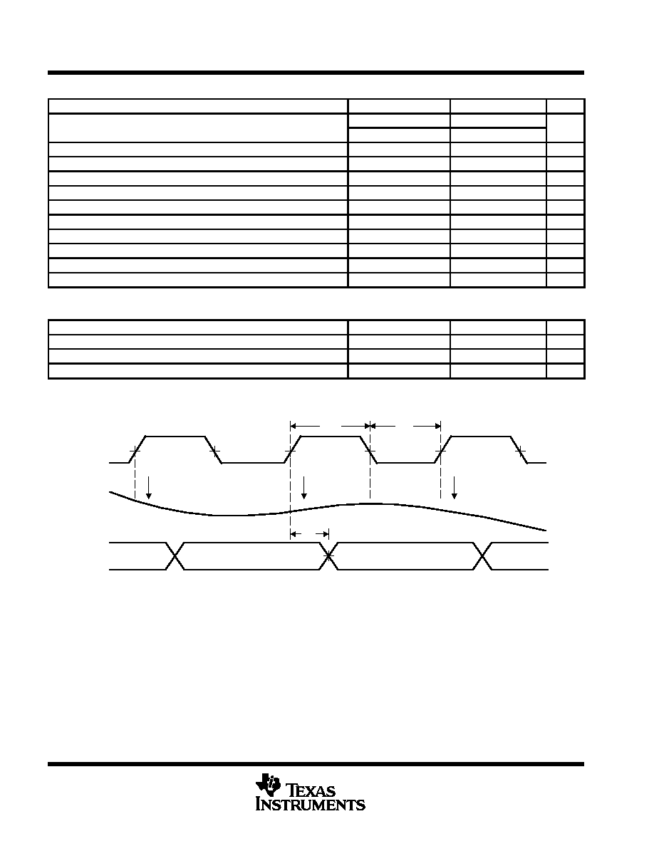
timing diagram
Data
N + 1
Data
N
N ≠ 1
Data
td
INPUT
D1 ≠ D6
ANLG
CLK
1.4 V
twL
twH
N + 2
N + 1
N
Sample
Sample
Sample

TL5501
6-BIT ANALOG-TO-DIGITAL CONVERTER
SLAS026 ≠ OCTOBER 1989 ≠ REVISED APRIL 1990
5
POST OFFICE BOX 655303
∑
DALLAS, TEXAS 75265
TYPICAL CHARACTERISTICS
4.984
5.000
4.992 V
4.968
4.520
4.504
4.488
4.024
4.008
3.992
See Note A
1/2 LSB
VFT = VFS
VFS
VZT
VZS + 1/2 LSB
VZS
Step
Digital Output CodeS
63
62
61
33
32
31
2
1
0
VI -- Analog Input Voltage -- V
111111
111110
S111101
100001
100000
011111
000000
000001
000010
IDEAL CONVERSION CHARACTERISTICS
NOTE A: This curve is based on the assumption that VrefB and Vref T have been
adjusted so that the voltage at the transition from digital 0 to 1 (VZT) is
4.000 V and the transition to full scale (VFT) is 4.992 V. 1 LSB = 16 mV.
Figure 1
Step
Digital Output Code
000010
000001
000000
011111
100000
100001
111101
111110
111111
VI -- Analog Input Voltage -- V
0
1
2
31
32
33
61
62
63
EL61
EL33
EL32
EL31
EL2
EL1
END-POINT LINEARITY ERROR
Figure 2