TL430
ADJUSTABLE SHUNT REGULATORS
SLVS050B JUNE 1976 REVISED JULY 1999
1
POST OFFICE BOX 655303
·
DALLAS, TEXAS 75265
D
Temperature Compensated
D
Programmable Output Voltage
D
Low Output Resistance
D
Low Output Noise
D
Sink Capability up to 100 mA
description
The TL430 is a 3-terminal adjustable shunt
regulator, featuring excellent temperature
stability, wide operating current range, and low
output noise. The output voltage can be set by two
external resistors to any desired value between
3 V and 30 V. The TL430 can replace zener diodes
in many applications, providing improved
performance.
The TL430C is characterized for operation from
0
°
C to 70
°
C.
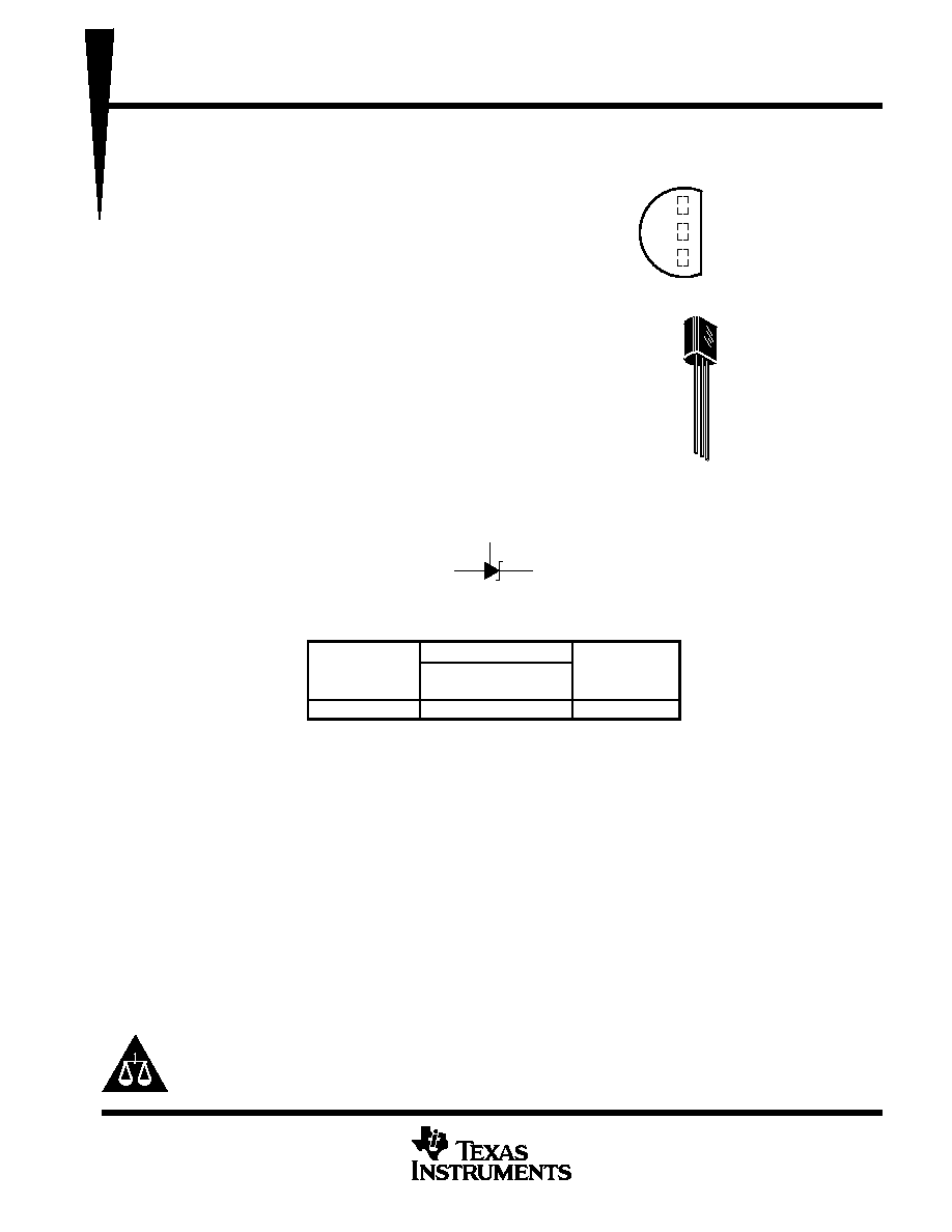
symbol
REF
CATHODE
ANODE
AVAILABLE OPTIONS
PACKAGED DEVICES
CHIP FORM
TA
PLASTIC
(LP)
CHIP FORM
(Y)
0
°
C to 70
°
C
TL430CLP
TL430Y
The LP package is available taped and reeled. Add R suffix to device
type (e.g., TL430CLPR). Chip forms are tested at 25
°
C.
Copyright
©
1999, Texas Instruments Incorporated
PRODUCTION DATA information is current as of publication date.
Products conform to specifications per the terms of Texas Instruments
standard warranty. Production processing does not necessarily include
testing of all parameters.
Please be aware that an important notice concerning availability, standard warranty, and use in critical applications of
Texas Instruments semiconductor products and disclaimers thereto appears at the end of this data sheet.
LP PACKAGE
(TOP VIEW)
REF
ANODE
CATHODE
TL430
ADJUSTABLE SHUNT REGULATORS
SLVS050B JUNE 1976 REVISED JULY 1999
2
POST OFFICE BOX 655303
·
DALLAS, TEXAS 75265
absolute maximum ratings over operating free-air temperature range (unless otherwise noted)
Regulator voltage (see Note 1)
30 V
. . . . . . . . . . . . . . . . . . . . . . . . . . . . . . . . . . . . . . . . . . . . . . . . . . . . . . . . . . . . . .
Continuous regulator current
150 mA
. . . . . . . . . . . . . . . . . . . . . . . . . . . . . . . . . . . . . . . . . . . . . . . . . . . . . . . . . . . . .
Package thermal impedance,
JA
(see Notes 2 and 3):
156
°
C/W
. . . . . . . . . . . . . . . . . . . . . . . . . . . . . . . . . . . .
Lead temperature 1,6 mm (1/16 inch) from case for 10 seconds
260
°
C
. . . . . . . . . . . . . . . . . . . . . . . . . . . . . . .
Storage temperature range, T
stg
65
°
C to 150
°
C
. . . . . . . . . . . . . . . . . . . . . . . . . . . . . . . . . . . . . . . . . . . . . . . . . . .
Stresses beyond those listed under "absolute maximum ratings" may cause permanent damage to the device. These are stress ratings only, and
functional operation of the device at these or any other conditions beyond those indicated under "recommended operating conditions" is not
implied. Exposure to absolute-maximum-rated conditions for extended periods may affect device reliability.
NOTES:
1. All voltage values are with respect to the anode terminal.
2. Maximum power dissipation is a function of TJ(max),
JA, and TA. The maximum allowable power dissipation at any allowable
ambient temperature is PD = (TJ(max) TA)/
JA. Operating at the absolute maximum TJ of 150
°
C can impact reliability.
3. The package thermal impedance is calculated in accordance with JESD 51, except for through-hole packages, which use a trace
length of zero.
recommended operating conditions
MIN
MAX
UNIT
Regulator voltage, VZ
Vref
30
V
Regulator current, IZ
2
100
mA
Operating free-air temperature range, TA
TL430C
0
70
°
C
electrical characteristics over recommended operating conditions, T
A
= 25
°
C (unless otherwise
noted)
PARAMETER
TEST
TEST CONDITIONS
TL430C
UNIT
PARAMETER
FIGURE
TEST CONDITIONS
MIN
TYP
MAX
UNIT
VI(ref)
Reference input voltage
1
VZ = VI(ref),
IZ = 10 mA
2.5
2.75
3
V
VI(ref)
Temperature coefficient of reference input
voltage
1
VZ = VI(ref),
TA = 0
°
C to 70
°
C
IZ = 10 mA,
120
ppm/
°
C
II(ref)
Reference input current
2
IZ = 10 mA,
R2 =
R1 = 10 k
,
3
10
µ
A
IZK
Regulator current near lower knee of
regulation range
1
VZ = VI(ref)
0.5
2
mA
IZK
Regulator current at maximum
1
VZ = VI(ref)
50
mA
IZK
g
limit of regulation range
2
VZ = 5 V to 30 V,
See Note 4
100
mA
rz
Differential regulator resistance
(see Note 5)
1
VZ = VI(ref),
IZ = (52 2) mA
1.5
3
W
VZ = 3 V
50
Vn
Noise voltage
2
f = 0.1 Hz to 10 Hz
VZ = 12 V
200
µ
V
VZ = 30 V
650
NOTES:
4. The average power dissipation, VZ
·
IZ
·
duty cycle, must not exceed the maximum continuous rating in any 10-ms interval.
5. The regulator resistance for VZ > VI(ref), rz, is given by:
rz
+
rz
1
)
R1
R2
TL430
ADJUSTABLE SHUNT REGULATORS
SLVS050B JUNE 1976 REVISED JULY 1999
3
POST OFFICE BOX 655303
·
DALLAS, TEXAS 75265
electrical characteristics over recommended operating conditions, T
A
= 25
°
C (unless otherwise
noted)
PARAMETER
TEST
TEST CONDITIONS
TL430Y
UNIT
PARAMETER
FIGURE
TEST CONDITIONS
MIN
TYP
MAX
UNIT
VI(ref)
Reference input voltage
1
VZ = VI(ref),
IZ = 10 mA
2.5
2.75
3
V
II(ref)
Reference input current
2
IZ = 10 mA,
R2 =
R1 = 10 k
,
3
10
µ
A
IZK
Regulator current near lower knee of
regulation range
1
VZ = VI(ref)
0.5
2
mA
IZK
Regulator current at maximum limit of
1
VZ = VI(ref)
50
mA
IZK
g
regulation range
2
VZ = 5 V to 30 V,
See Note 4
100
mA
rz
Differential regulator resistance (see Note 5)
1
VZ = VI(ref), . . .
IZ = (52 2) mA
1.5
3
W
VZ = 3 V
50
Vn
Noise voltage
2
f = 0.1 Hz to 10 Hz
VZ = 12 V
200
µ
V
VZ = 30 V
650
NOTES:
4. The average power dissipation, VZ
·
IZ
·
duty cycle, must not exceed the maximum continuous rating in any 10-ms interval.
5. The regulator resistance for VZ > VI(ref), rz, is given by:
rz
+
rz
1
)
R1
R2
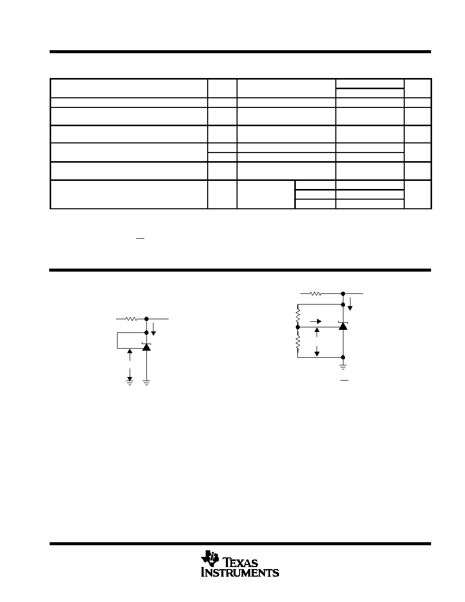
PARAMETER MEASUREMENT INFORMATION
V
Z
+
V
I(ref)
1
)
R1
R2
)
I
I(ref)
R1
VI(ref)
Input
VZ
IZ
II(ref)
IZ
VZ
Input
VI(ref)
R1
R2
TL430
TL430
Figure 1. Test Circuit for V
Z
= V
I(ref)
Figure 2. Test Circuit for V
Z
> V
I(ref)