Document Outline
- FEATURES
- APPLICATIONS
- DESCRIPTION
- Function Tables
- Terminal Functions
- SN65HVD230, SN65HVD231
- SN65HVD232
- equivalent input and output schematic diagrams
- absolute maximum ratings over operating free-air temperature (see Note \
1) (unless otherwise
noted) Å
- recommended operating conditions
- ELECTRICAL SPECIFICATIONS
- driver electrical characteristics over recommended operating conditions \
(unless otherwise noted)
- driver switching characteristics over recommended operating conditions(\
unless otherwise noted)
- SN65HVD230 and SN65HVD231
- SN65HVD232
- receiver electrical characteristics over recommended operating condition\
s (unless otherwise noted)
- receiver switching characteristics over recommended operating conditions\
(unless otherwise noted)
- device switching characteristics over recommended operating conditions (\
unless otherwise noted)
- device control-pin characteristics over recommended operating conditions\
(unless otherwise noted)
- PARAMETER MEASUREMENT INFORMATION
- TYPICAL CHARACTERISTICS
- APPLICATION INFORMATION
- introduction
- application of the SN65HVD230
- features of the SN65HVD230, SN65HVD231, and SN65HVD232
- operating modes
- high-speed
- slope control
- standby mode (listen only mode) of the HVD230
- the babbling idiot protection of the HVD230
- sleep mode of the HVD231
- loop propagation delay
- interoperability with 5-V CAN systems
- MECHANICAL DATA
- D (R-PDSO-G**) PLASTIC SMALL-OUTLINE PACKAGE
- IMPORTANT NOTICE

SN65HVD230
SN65HVD231
SN65HVD232
SLOS346G ≠ MARCH 2001 ≠ REVISED JUNE 2002
3.3-V CAN TRANSCEIVERS
1
www.ti.com
FEATURES
D
Operates With a 3.3-V Supply
D
Low Power Replacement for the PCA82C250
Footprint
D
Bus/Pin ESD Protection Exceeds 16 kV HBM
D
High Input Impedance Allows for 120 Nodes
on a Bus
D
Controlled Driver Output Transition Times for
Improved Signal Quality on the SN65HVD230
and SN65HVD231
D
Unpowered Node Does Not Disturb the Bus
D
Compatible With the Requirements of the
ISO 11898 Standard
D
Low-Current SN65HVD230 Standby Mode
370
µ
A Typical
D
Low-Current SN65HVD231 Sleep Mode
40 nA Typical
D
Designed for Signaling Rates
up to
1 Megabit/Second (Mbps)
D
Thermal Shutdown Protection
D
Open-Circuit Fail-Safe Design
D
Glitch-Free Power-Up and Power-Down
Protection for Hot-Plugging Applications
APPLICATIONS
D
Motor Control
D
Industrial Automation
D
Basestation Control and Status
D
Robotics
D
Automotive
D
UPS Control
LOGIC DIAGRAM (POSITIVE LOGIC)
CANL
CANH
R
D
1
4
7
6
SN65HVD230, SN65HVD231
Logic Diagram (Positive Logic)
RS
8
Vref
5
3
VCC
CANL
CANH
R
D
1
4
7
6
SN65HVD232
Logic Diagram (Positive Logic)
The signaling rate of a line is the number of voltage transitions that are made per second expressed in the units bps (bits per second).
PRODUCTION DATA information is current as of publication date.
Products conform to specifications per the terms of Texas Instruments
standard warranty. Production processing does not necessarily include
testing of all parameters.
Copyright
2002, Texas Instruments Incorporated
Please be aware that an important notice concerning availability, standard warranty, and use in critical applications of Texas Instruments
semiconductor products and disclaimers thereto appears at the end of this data sheet.
D
GND
V
CC
R
R
S
CANH
CANL
V
ref
SN65HVD230D (Marked as VP230)
SN65HVD231D (Marked as VP231)
(TOP VIEW)
1
2
3
4
8
7
6
5
NC ≠ No internal connection
D
GND
V
CC
R
NC
CANH
CANL
NC
SN65HVD232D (Marked as VP232)
(TOP VIEW)
1
2
3
4
8
7
6
5
TMS320Lx240x is a trademark of Texas Instruments.
SN65HVD230
SN65HVD231
SN65HVD232
SLOS346G ≠ MARCH 2001 ≠ REVISED JUNE 2002
2
www.ti.com
DESCRIPTION
The SN65HVD230, SN65HVD231, and SN65HVD232 controller area network (CAN) transceivers are designed
for use with the Texas Instruments TMS320Lx240x
3.3-V DSPs with CAN controllers, or with equivalent
devices. They are intended for use in applications employing the CAN serial communication physical layer in
accordance with the ISO 11898 standard. Each CAN transceiver is designed to provide differential transmit
capability to the bus and differential receive capability to a CAN controller at speeds up to 1 Mbps.
Designed for operation in especially-harsh environments, these devices feature cross-wire protection,
loss-of-ground and overvoltage protection, overtemperature protection, as well as wide common-mode range.
The transceiver interfaces the single-ended CAN controller with the differential CAN bus found in industrial,
building automation, and automotive applications. It operates over a ≠ 2-V to 7-V common-mode range on the
bus, and it can withstand common-mode transients of
±
25 V.
On the SN65HVD230 and SN65HVD231, pin 8 provides three different modes of operation: high-speed, slope
control, and low-power modes. The high-speed mode of operation is selected by connecting pin 8 to ground,
allowing the transmitter output transistors to switch on and off as fast as possible with no limitation on the rise
and fall slopes. The rise and fall slopes can be adjusted by connecting a resistor to ground at pin 8, since the
slope is proportional to the pin's output current. This slope control is implemented with external resistor values
of 10 k
,
to achieve a 15-V/
µ
s slew rate, to 100 k
,
to achieve a 2-V/
µ
s slew rate. See the Application
Information section of this data sheet.
The circuit of the SN65HVD230 enters a low-current standby mode during which the driver is switched off and
the receiver remains active if a high logic level is applied to pin 8. The DSP controller reverses this low-current
standby mode when a dominant state (bus differential voltage > 900 mV typical) occurs on the bus.
The unique difference between the SN65HVD230 and the SN65HVD231 is that both the driver and the receiver
are switched off in the SN65HVD231 when a high logic level is applied to pin 8 and remain in this sleep mode
until the circuit is reactivated by a low logic level on pin 8.
The V
ref
pin 5 on the SN65HVD230 and SN65HVD231 is available as a V
CC
/2 voltage reference.
The SN65HVD232 is a basic CAN transceiver with no added options; pins 5 and 8 are NC, no connection.
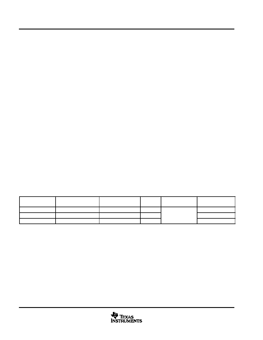
AVAILABLE OPTIONS
PART NUMBER
LOW
POWER MODE
INTEGRATED SLOPE
CONTROL
Vref PIN
TA
MARKED AS:
SN65HVD230
Standby mode
Yes
Yes
VP230
SN65HVD231
Sleep mode
Yes
Yes
≠ 40
∞
C to 85
∞
C
VP231
SN65HVD232
No standby or sleep mode
No
No
40 C to 85 C
VP232

SN65HVD230
SN65HVD231
SN65HVD232
SLOS346G ≠ MARCH 2001 ≠ REVISED JUNE 2002
3
www.ti.com
Function Tables
DRIVER (SN65HVD230, SN65HVD231)
INPUT D
R
OUTPUTS
BUS STATE
INPUT D
RS
CANH
CANL
BUS STATE
L
V
1 2 V
H
L
Dominant
H
V(Rs) < 1.2 V
Z
Z
Recessive
Open
X
Z
Z
Recessive
X
V(Rs) > 0.75 VCC
Z
Z
Recessive
H = high level; L = low level; X = irrelevant; ? = indeterminate; Z = high impedance
DRIVER (SN65HVD232)
INPUT D
OUTPUTS
BUS STATE
INPUT D
CANH
CANL
BUS STATE
L
H
L
Dominant
H
Z
Z
Recessive
Open
Z
Z
Recessive
H = high level; L = low level; Z = high impedance
RECEIVER (SN65HVD230)
DIFFERENTIAL INPUTS
RS
OUTPUT R
VID
0.9 V
X
L
0.5 V < VID < 0.9 V
X
?
VID
0.5 V
X
H
Open
X
H
H = high level; L = low level; X = irrelevant; ? = indeterminate
RECEIVER (SN65HVD231)
DIFFERENTIAL INPUTS
RS
OUTPUT R
VID
0.9 V
L
0.5 V < VID < 0.9 V
V(Rs) < 1.2 V
?
VID
0.5 V
V(Rs) < 1.2 V
H
X
V(Rs) > 0.75 VCC
H
X
1.2 V < V(Rs) < 0.75 VCC
?
Open
X
H
H = high level; L = low level; X = irrelevant; ? = indeterminate
RECEIVER (SN65HVD232)
DIFFERENTIAL INPUTS
OUTPUT R
VID
0.9 V
L
0.5 V < VID < 0.9 V
?
VID
0.5 V
H
Open
H
H = high level; L = low level; X = irrelevant;
? = indeterminate

SN65HVD230
SN65HVD231
SN65HVD232
SLOS346G ≠ MARCH 2001 ≠ REVISED JUNE 2002
4
www.ti.com
Function Tables (Continued)
TRANSCEIVER MODES (SN65HVD230, SN65HVD231)
V(Rs)
OPERATING MODE
V(Rs) > 0.75 VCC
Standby
10 k
to 100 k
to ground
Slope control
V(Rs) < 1 V
High speed (no slope control)
Terminal Functions
SN65HVD230, SN65HVD231
TERMINAL
DESCRIPTION
NAME
NO.
DESCRIPTION
CANL
6
Low bus output
CANH
7
High bus output
D
1
Driver input
GND
2
Ground
R
4
Receiver output
RS
8
Standby/slope control
VCC
3
Supply voltage
Vref
5
Reference output
SN65HVD232
TERMINAL
DESCRIPTION
NAME
NO.
DESCRIPTION
CANL
6
Low bus output
CANH
7
High bus output
D
1
Driver input
GND
2
Ground
NC
5, 8
No connection
R
4
Receiver output
VCC
3
Supply voltage

SN65HVD230
SN65HVD231
SN65HVD232
SLOS346G ≠ MARCH 2001 ≠ REVISED JUNE 2002
5
www.ti.com
equivalent input and output schematic diagrams
VCC
D Input
1 k
9 V
Input
100 k
VCC
Output
16 V
CANH and CANL Outputs
20 V
VCC
5
9 V
Output
R Output
VCC
Input
16 V
CANH and CANL Inputs
20 V
110 k
45 k
9 k
9 k