 | –≠–ª–µ–∫—Ç—Ä–æ–Ω–Ω—ã–π –∫–æ–º–ø–æ–Ω–µ–Ω—Ç: PCI4450 | –°–∫–∞—á–∞—Ç—å:  PDF PDF  ZIP ZIP |

PCI4450 GFN/GJG
PC Card and OHCI Controller
SCPS046 ≠ JANUARY 1999
1
POST OFFICE BOX 655303
∑
DALLAS, TEXAS 75265
D
1997 PC Standard Compliant
D
PCI Bus Power Management Interface
Specification 1.1 Compliant
D
ACPI 1.0 Compliant
D
PCI Local Bus Specification Revision
2.1/2.2 Compliant
D
PC 98/99 Compliant
D
Compliant with the PCI Bus Interface
Specification for PCI-to-CardBus Bridges
D
Fully Compliant with the PCI Bus Power
Management Specification for PCI to
CardBus Bridges Specification
D
Ultra Zoomed Video
D
Zoomed Video Auto-Detect
D
Advanced filtering on Card Detect Lines
Provide 90 Microseconds of Noise
Immunity.
D
Programmable D3 Status Pin
D
Internal Ring Oscillator
D
3.3-V Core Logic with Universal PCI
Interfaces Compatible with 3.3-V and 5-V
PCI Signaling Environments
D
Mix-and-Match 5-V/3.3-V PC Card16 Cards
and 3.3-V CardBus Cards
D
Supports Two PC Card or CardBus Slots
With Hot Insertion and Removal
D
Uses Serial Interface to TI
TM
TPS2206 Dual
Power Switch
D
Supports 132 Mbyte/sec. Burst Transfers
to Maximize Data Throughput on Both the
PCI Bus and the CardBus Bus
D
Supports Serialized IRQ with PCI
Interrupts
D
8 Programmable Multifunction Pins
D
Interrupt Modes Supported: Serial
ISA/Serial PCI, Serial ISA/Parallel PCI,
Parallel PCI Only.
D
Serial EEPROM Interface for Loading
Subsystem ID and Subsystem Vendor ID
D
Supports Zoomed Video with Internal
Buffering
D
Dedicated Pin for PCI CLKRUN
D
Four General-Purpose Event Registers
D
Multifunction PCI Device with Separate
Configuration Space for each Socket
D
Five PCI Memory Windows and Two I/O
Windows Available to each PC Card16
Socket
D
Two I/O Windows and Two Memory
Windows Available to each CardBus
Socket
D
ExCA
TM
-Compatible Registers are Mapped
in Memory or I/O Space
D
Supports Distributed DMA and PC/PCI
DMA
D
Intel
TM
82365SL-DF Register Compatible
D
Supports 16-bit DMA on Both PC Card
Sockets
D
Supports Ring Indicate, SUSPEND, and
PCI CLKRUN
D
Advanced Submicron, Low-Power CMOS
Technology
D
Provides VGA / Palette Memory and I/O,
and Subtractive Decoding Options
D
LED Activity Pins
D
Supports PCI Bus Lock (LOCK)
D
Packaged in a 256-pin BGA or 257-pin
Micro-Star BGA
D
OHCI Link Function Designed to IEEE 1394
Open Host Controller Interface (OHCI)
Specification
D
Implements PCI Burst Transfers and Deep
FIFOs to Tolerate Large Host Latency
D
Supports Physical Write Posting of up to 3
Outstanding Transactions
D
OHCI Link Function is IEEE 1394-1995
Compliant and Compatible with
Proposal 1394a
D
Supports Serial Bus Data Rates of 100,
200, and 400 Mbits/second
D
Provides Bus-Hold Buffers on the
PHY-Link I/F for Low-cost Single Capacitor
Isolation
Copyright
©
1999, Texas Instruments Incorporated
PRODUCTION DATA information is current as of publication date.
Products conform to specifications per the terms of Texas Instruments
standard warranty. Production processing does not necessarily include
testing of all parameters.
Please be aware that an important notice concerning availability, standard warranty, and use in critical applications of
Texas Instruments semiconductor products and disclaimers thereto appears at the end of this data sheet.
Intel is a trademark of Intel Corporation.
PC Card is a trademark of Personal Computer Memory Card International Association (PCMCIA).
TI is a trademark of Texas Instruments Incorporated.

PCI4450 GFN/GJG
PC Card and OHCI Controller
SCPS046 ≠ JANUARY 1999
2
POST OFFICE BOX 655303
∑
DALLAS, TEXAS 75265
Description
3
. . . . . . . . . . . . . . . . . . . . . . . . . . . . . . . . . . . . . . . . . . . .
Terminal Assignments
4
. . . . . . . . . . . . . . . . . . . . . . . . . . . . . . . . . . .
Signal Names and Terminal Assignments
5
. . . . . . . . . . . . . . . . . . .
PCI4450 System Block Diagram
9
. . . . . . . . . . . . . . . . . . . . . . . . . . .
Terminal Functions
10
. . . . . . . . . . . . . . . . . . . . . . . . . . . . . . . . . . . .
I/O Characteristics
23
. . . . . . . . . . . . . . . . . . . . . . . . . . . . . . . . . . . .
Clamping Voltages
23
. . . . . . . . . . . . . . . . . . . . . . . . . . . . . . . . . . . .
PCI Interface
24
. . . . . . . . . . . . . . . . . . . . . . . . . . . . . . . . . . . . . . . . .
PC Card Applications Overview
28
. . . . . . . . . . . . . . . . . . . . . . . . .
Programmable Interrupt Subsystem
35
. . . . . . . . . . . . . . . . . . . . . .
Power Management Overview
38
. . . . . . . . . . . . . . . . . . . . . . . . . .
PC Card Controller Programming Model
43
. . . . . . . . . . . . . . . . . .
PCI Configuration Registers (Functions 0 and 1)
44
. . . . . . . . . . .
ExCA Compatibility Registers (Functions 0 and 1)
82
. . . . . . . . . .
CardBus Socket Registers (Functions 0 and 1)
106
. . . . . . . . . . .
Distributed DMA (DDMA) Registers
114
. . . . . . . . . . . . . . . . . . . . . .
GPIO Interface
182
. . . . . . . . . . . . . . . . . . . . . . . . . . . . . . . . . . . . . . . . .
Serial EEPROM
183
. . . . . . . . . . . . . . . . . . . . . . . . . . . . . . . . . . . . . . . .
Absolute Maximum Ratings
185
. . . . . . . . . . . . . . . . . . . . . . . . . . . . . . .
Recommended Operating Conditions
186
. . . . . . . . . . . . . . . . . . . . . . .
Electrical Characteristics
187
. . . . . . . . . . . . . . . . . . . . . . . . . . . . . . . . .
PCI Clock/Reset Timing Requirements
188
. . . . . . . . . . . . . . . . . . . . .
PCI Timing Requirements
188
. . . . . . . . . . . . . . . . . . . . . . . . . . . . . . . .
Switrching Characteristics for PHY-Link Interface
188
. . . . . . . . . . . . .
Parameter Measurement Information
189
. . . . . . . . . . . . . . . . . . . . . . .
PCI Bus Parameter Measurement Information
190
. . . . . . . . . . . . . . .
PC Card Cycle Timing
191
. . . . . . . . . . . . . . . . . . . . . . . . . . . . . . . . . . .
Timing Requirements, (Memory Cycles)
192
. . . . . . . . . . . . . . . . . . . .
Timing Requirements, (I/O Cycles)
197
. . . . . . . . . . . . . . . . . . . . . . . . .
Switching Characteristics (Miscellaneous)
193
. . . . . . . . . . . . . . . . . .
PC Card Parameter Mesasurement Information
193
. . . . . . . . . . . . . .
Mechanical Data
195
. . . . . . . . . . . . . . . . . . . . . . . . . . . . . . . . . . . . . . . .
Table of Contents

PCI4450 GFN/GJG
PC Card and OHCI Controller
SCPS046 ≠ JANUARY 1999
3
POST OFFICE BOX 655303
∑
DALLAS, TEXAS 75265
description
The Texas Instruments PCI4450 is an integrated dual-socket PC Card controller and IEEE 1394 Open HCI host
controller. This high-performance integrated solution provides the latest in both PC Card and IEEE 1394
technology.
The PCI4450 is a three-function PCI device compliant with
PCI Local Bus Specification 2.2. Functions 0 and
1 provide the independent PC Card socket controllers compliant with the 1997 PC Card Standard. The PCI4450
provides features that make it the best choice for bridging between the PCI bus and PC Cards, and supports
any combination of 16-bit and CardBus PC Cards in the two sockets, powered at 5 V or 3.3 V, as required.
All card signals are internally buffered to allow hot insertion and removal without external buffering. The
PCI4450 is register compatible with the Intel 82365SL≠DF ExCA controller. The PCI4450 internal data path
logic allows the host to access 8-, 16-, and 32-bit cards using full 32-bit PCI cycles for maximum performance.
Independent buffering and a pipeline architecture provide an unsurpassed performance level with sustained
bursting. The PCI4450 can be programmed to accept posted writes to improve bus utilization.
Function 2 of the PCI4450 is compatible with IEEE1394A and the latest 1394 open host controller interface
(OHCI) specifications. The chip provides the IEEE1394 link function and is compatible with data rates of 100,
200, and 400 Mbits per second. Deep FIFOs are provided to buffer 1394 data and accommodate large host
bus latencies. The PCI4450 provides physical write posting and a highly tuned physical data path for SBP-2
performance. Multiple cache line burst transfers, advanced internal arbitration, and bus holding buffers on the
PHY/Link interface are other features that make the PCI4450 the best-in-class 1394 Open HCI solution.
The PCI4450 provides an internally buffered zoomed video (ZV) path. This reduces the design effort of PC
board manufacturers to add a ZV-compatible solution and guarantees compliance with the CardBus loading
specifications.
Various implementation specific functions and general-purpose inputs and outputs are provided through eight
multifunction terminals. These terminals present a system with options in PC/PCI DMA, PCI LOCK and parallel
interrupts, PC Card activity indicator LEDs, and other platform specific signals. ACPI-complaint
general-purpose events may be programmed and controlled through the multifunction terminals, and an
ACPI-compliant programming interface is included for the general-purpose inputs and outputs.
The PCI4450 is compliant with the latest
PCI Bus Power Management Specification, and provides several
low-power modes which enable the host power system to further reduce power consumption. The
PC Card
(CardBus) Controller and IEEE 1394 Host Controller Device Class Specifications required for Microsoft
OnNow
t
Power Management are supported. Furthermore, an advanced complementary metal-oxide
semiconductor (CMOS) process achieves low system power consumption.
Unused PCI4450 inputs must be pulled to a valid logic level using a 43 k
resistor.
use of symbols in this document
Throughout this data sheet the overbar symbol denotes an active-low signal. For example: FRAME denotes
that this is an active-low signal.
PCI4450 GFN/GJG
PC Card and OHCI Controller
SCPS046 ≠ JANUARY 1999
4
POST OFFICE BOX 655303
∑
DALLAS, TEXAS 75265
terminal assignments
B
B
B
B
B
B
B
B
B
B
B
A
A
A
A
A
A
A
««
««
B
B
B
B
B
B
B
B
B
B
B
A
A
A
A
A
A
A
A
B
B
B
B
B
B
B
B
B
B
B
A
A
A
A
A
A
A
A
B
B
««
««
B
B
««
««
B
B
B
««
««
A
A
««
««
A
A
A
B
B
B
A
A
A
A
B
B
A
A
A
B
B
B
A
A
A
B
B
««
««
««
««
A
A
A
B
B
B
A
A
A
P
P
P
A
A
A
P
P
A
A
A
A
P
P
P
A
A
A
A
P
P
««
««
««
««
A
A
A
P
P
P
Z
Z
A
A
P
P
Z
Z
A
P
P
P
Z
Z
Z
Z
P
P
««
««
P
P
««
««
T
S
««
««
S
««
««
Z
Z
Z
P
P
P
P
P
P
P
T
S
S
S
S
Z
Z
Z
Z
P
P
P
P
P
P
T
S
S
S
S
S
Z
Z
Z
Z
P
P
P
P
P
P
S
S
S
S
Z
Z
Z
20
19
18
17
16
15
14
13
12
11
10
9
8
7
6
5
4
3
2
1
B
B
B
B
B
B
B
B
B
P
P
P
P
P
P
P
P
P
P
P
A
B
C
D
E
F
G
H
J
K
L
M
N
P
R
T
U
V
W
Y
Bottom View
S
1394 PHY/Link
P
A
B
Z
PCI Interface
PC Card A
PC Card B
Zoom Video
««
T
V
CC
3.3 Volt
Ground (GND)
TPS Power Switch
Miscellaneous
A
A
Z
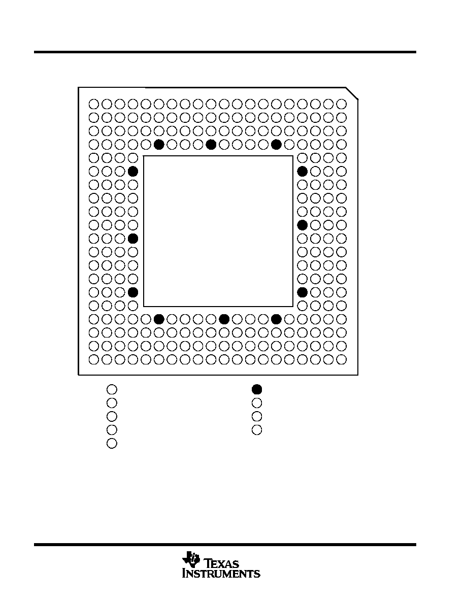
Figure 1. PCI4450 Pin Diagram
PCI4450 GFN/GJG
PC Card and OHCI Controller
SCPS046 ≠ JANUARY 1999
5
POST OFFICE BOX 655303
∑
DALLAS, TEXAS 75265
signal names and terminal assignments
Signal names and their terminal assignments are shown in Tables 1 and 2 and are sorted alphanumerically by
the assigned terminal.
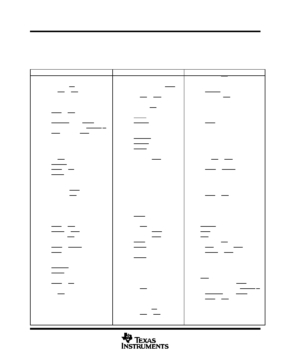
Table 1. GFN Terminals Sorted Alphanumerically for CardBus // 16-bit Signals and OHCI
GFN
SIGNAL NAME
GFN
SIGNAL NAME
GFN
SIGNAL NAME
A1
A2
A3
A4
A5
A6
A7
A8
A9
A10
A11
A12
A13
A14
A15
A16
A17
A18
A19
A20
B1
B2
B3
B4
B5
B6
B7
B8
B9
B10
B11
B12
B13
B14
B15
B16
B17
B18
B19
B20
C1
C2
C3
C4
C5
C6
C7
C8
GND
A_CAD16//A_A17
A_CAD11//A_OE
A_CC/BE0//A_CE1
A_RSVD//A_D14
A_CAD3//A_D5
A_CAD1//A_D4
A_CCD1//A_CD1
B_CAD29//B_D1
B_CCLKRUN//B_WP(IOIS16)
B_CSTSCHG//B_BVD1(STSCHG/RI)
B_CINT//B_READY(IREQ)
B_CAD24//B_A2
B_CAD23//B_A3
B_CAD21//B_A5
B_CAD19//B_A25
B_CC/BE2//B_A12
B_CFRAME//B_A23
B_CGNT//B_WE
B_CSTOP//B_A20
A_RSVD//A_A18
A_CAD14//A_A9
A_CAD15//A_IOWR
A_CAD10//A_CE2
VCCA
A_CAD5//A_D6
A_CAD4//A_D12
A_CAD0//A_D3
B_CAD30//B_D9
B_CCD2//B_CD2
B_CSERR//B_WAIT
B_CVS1//B_VS1
VCCB
B_CREQ//B_INPACK
B_CRST//B_RESET
B_CAD18//B_A7
B_CCLK//B_A16
B_CDEVSEL//B_A21
B_CPERR//B_A14
B_CPAR//B_A13
A_CGNT//A_WE
A_CPAR//A_A13
A_CC/BE1//A_A8
A_CAD12//A_A11
A_CAD9//A_A10
A_CAD8//A_D15
A_CAD6//A_D13
A_CAD2//A_D11
C9
C10
C11
C12
C13
C14
C15
C16
C17
C18
C19
C20
D1
D2
D3
D4
D5
D6
D7
D8
D9
D10
D11
D12
D13
D14
D15
D16
D17
D18
D19
D20
E1
E2
E3
E4
E17
E18
E19
E20
F1
F2
F3
F4
F17
F18
F19
F20
B_RSVD//B_D2
B_CAD27//B_D0
B_CAUDIO//B_BVD2(SPKR)
B_CAD26//B_A0
B_CC/BE3//B_REG
B_CAD22//B_A4
B_CVS2//B_VS2
B_CAD17//B_A24
B_CTRDY//B_A22
B_CBLOCK//B_A19
B_RSVD//B_A18
B_CAD14//B_A9
A_CDEVSEL//A_A21
A_CBLOCK//A_A19
A_CPERR//A_A14
GND
A_CAD13//A_IORD
VCC
A_CAD7//A_D7
GND
B_CAD31//B_D10
B_CAD28//B_D8
VCC
B_CAD25//B_A1
GND
B_CAD20//B_A6
VCC
B_CIRDY//B_A15
GND
B_CC/BE1//B_A8
B_CAD15//B_IOWR
B_CAD13//B_IORD
A_CIRDY//A_A15
A_CTRDY//A_A22
A_CCLK//A_A16
A_CSTOP//A_A20
B_CAD16//B_A17
B_CAD12//B_A11
VCCB
B_CAD9//B_A10
A_CAD17//A_A24
A_CC/BE2//A_A12
VCCA
VCC
VCC
B_CAD11//B_OE
B_CC/BE0//B_CE1
B_CAD7//B_D7
G1
G2
G3
G4
G17
G18
G19
G20
H1
H2
H3
H4
H17
H18
H19
H20
J1
J2
J3
J4
J17
J18
J19
J20
K1
K2
K3
K4
K17
K18
K19
K20
L1
L2
L3
L4
L17
L18
L19
L20
M1
M2
M3
M4
M17
M18
M19
M20
A_CVS2//A_VS2
A_CAD19//A_A25
A_CAD18//A_A7
A_CFRAME//A_A23
B_CAD10//B_CE2
B_CAD8//B_D15
B_RSVD//B_D14
B_CAD5//B_D6
A_CAD21//A_A5
A_CRST//A_RESET
A_CAD20//A_A6
GND
GND
B_CAD6//B_D13
B_CAD3//B_D5
B_CAD4//B_D12
A_CC/BE3//A_REG
A_CAD23//A_A3
A_CREQ//A_INPACK
A_CAD22//A_A4
B_CAD1//B_D4
B_CAD2//B_D11
B_CAD0//B_D3
B_CCD1//B_CD1
A_CAD26//A_A0
A_CAD24//A_A2
A_CAD25//A_A1
VCC
PCLK
CLKRUN
PRST
GNT
A_CVS1//A_VS1
A_CINT//A_READY(IREQ)
A_CSERR//A_WAIT
VCCA
VCC
AD31
AD30
REQ
A_CAUDIO//A_BVD2(SPKR)
A_CSTSCHG//A_BVD1(STSCHG/RI)
A_CCLKRUN//A_WP(IOIS16)
A_CCD2//A_CD2
AD26
AD27
AD28
AD29