 | –≠–ª–µ–∫—Ç—Ä–æ–Ω–Ω—ã–π –∫–æ–º–ø–æ–Ω–µ–Ω—Ç: LOG102 | –°–∫–∞—á–∞—Ç—å:  PDF PDF  ZIP ZIP |
FEATURES
q
EASY-TO-USE COMPLETE LOG RATIO FUNCTION
q
OUTPUT AMPLIFIERS FOR SCALING AND
SIGNAL LOSS INDICATION
q
HIGH ACCURACY: 0.15% FSO Total Error Over
6 Decades
q
WIDE INPUT DYNAMIC RANGE:
6 Decades, 1nA to 1mA
q
LOW QUIESCENT CURRENT: 1.25mA
q
SO-14 PACKAGE
Precision
LOGARITHMIC AND LOG RATIO AMPLIFIER
DESCRIPTION
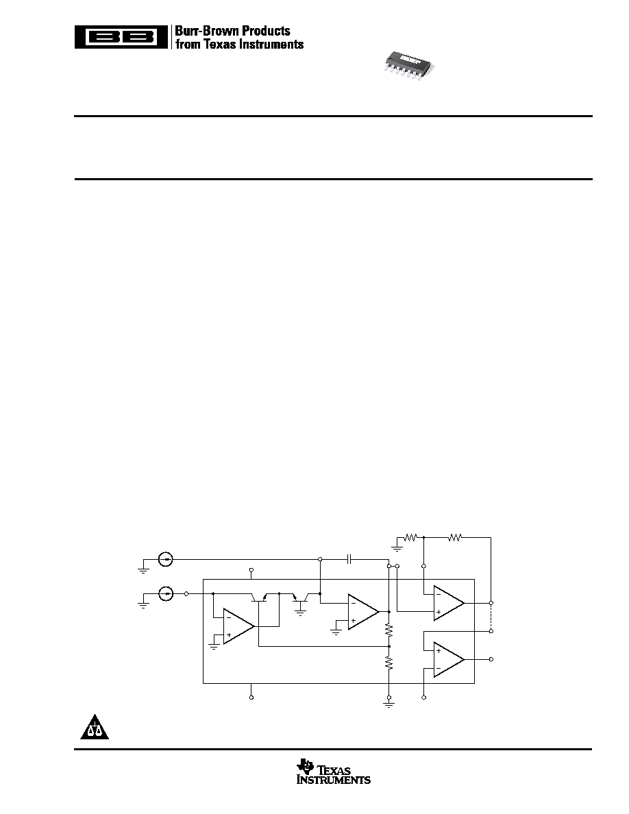
The LOG102
is a versatile integrated circuit that computes
the logarithm or log ratio of an input current relative to a
reference current.
The LOG102 is tested over a wide dynamic range of input
signals. In log ratio applications, a signal current can be
generated by a photodiode, and a reference current from a
resistor in series with a precision external voltage reference.
A3 and A4 are identical, uncommitted op amps that can be
used for a variety of functions, such as filtering, offsetting,
adding gain or as a comparator to detect loss of signal.
The output signal at V
LOG OUT
is trimmed to 1V
per decade of
input current. It can be scaled with an output amplifier, either
A3 or A4.
Low dc offset voltage and temperature drift allow accurate
measurement of low-level signals over a wide environmental
temperature range. The LOG102 is specified over the tem-
perature range, 0
∞
C to +70
∞
C, with operation over ≠40
∞
C to
+85
∞
C.
APPLICATIONS
q
ONET, OPTICAL POWER METERS
q
LOG, LOG RATIO COMPUTATION:
Communication, Analytical, Medical, Industrial,
Test, General Instrumentation
q
PHOTODIODE SIGNAL COMPRESSION AMP
q
ANALOG SIGNAL COMPRESSION IN FRONT
OF A/D CONVERTER
q
ABSORBANCE MEASUREMENT
q
OPTICAL DENSITY MEASUREMENT
LOG102
www.ti.com
PRODUCTION DATA information is current as of publication date.
Products conform to specifications per the terms of Texas Instruments
standard warranty. Production processing does not necessarily include
testing of all parameters.
Copyright © 2001, Texas Instruments Incorporated
SBOS211A ≠ MARCH 2002
A
2
A
3
A
1
I
1
Q
1
Q
2
VOUT3
A
4
VOUT4
+IN4
≠IN4
≠IN3
+IN3
V
LOG OUT
V
LOG OUT
= LOG (I
1
/I
2
)
V
OUT3
= G ∑ LOG (I
1
/I
2
), G = 1 +R
2
/R
1
R
1
R
2
C
C
I
2
A4 can be used
as comparator for
signal loss detect.
V≠
V+
6
14
1
9
11
4
7
12
8
3
5
10
GND
NOTE: U.S. Patent Pending.
LOG102
Please be aware that an important notice concerning availability, standard warranty, and use in critical applications of
Texas Instruments semiconductor products and disclaimers thereto appears at the end of this data sheet.
www.ti.com
LOG102
2
SBOS211A
SPECIFIED
PACKAGE
TEMPERATURE
PACKAGE
ORDERING
TRANSPORT
PRODUCT
PACKAGE-LEAD
DESIGNATOR
(1)
RANGE
MARKING
NUMBER
MEDIA, QUANTITY
LOG102AID
SO -14
D
0
∞
C to +70
∞
C
LOG102A
LOG102AID
Rails, 58
"
"
"
"
"
LOG102AIDR
Tape and Reel, 2500
NOTES: (1) For the most current specifications and package information, refer to our web site at www.ti.com.
ELECTROSTATIC
DISCHARGE SENSITIVITY
This integrated circuit can be damaged by ESD. Texas Instru-
ments recommends that all integrated circuits be handled with
appropriate precautions. Failure to observe proper handling
and installation procedures can cause damage.
ESD damage can range from subtle performance degrada-
tion to complete device failure. Precision integrated circuits
may be more susceptible to damage because very small
parametric changes could cause the device not to meet its
published specifications.
ABSOLUTE MAXIMUM RATINGS
(1)
Supply Voltage, V+ to V≠ .................................................................... 36V
Input Voltage ....................................................... V≠ (≠0.5) to V+ (+0.5V)
Input Current ...................................................................................
±
10mA
Output Short-Circuit
(2)
.............................................................. Continuous
Operating Temperature .................................................... ≠40
∞
C to +85
∞
C
Storage Temperature ..................................................... ≠55
∞
C to +125
∞
C
Junction Temperature .................................................................... +150
∞
C
Lead Temperature (soldering, 10s) ............................................... +300
∞
C
NOTES: (1) Stresses above these ratings may cause permanent damage.
Exposure to absolute maximum conditions for extended periods may degrade
device reliability. (2) Short circuit to ground, one amplifier per package.
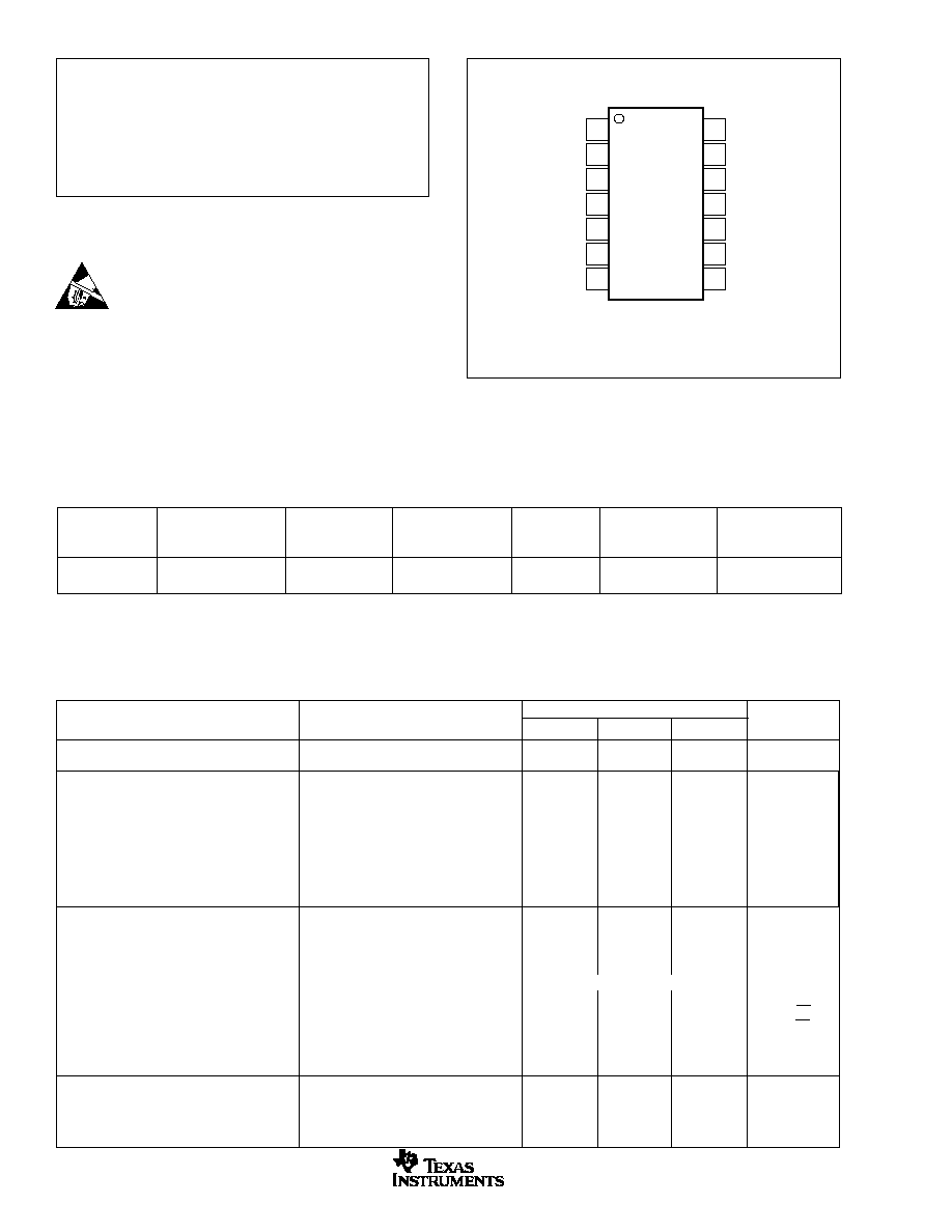
PACKAGE/ORDERING INFORMATION
I
2
NC
+IN4
≠IN4
GND
V≠
VOUT4
NC = No Internal Connection
LOG102
I
1
NC
+IN3
≠IN3
Vlog out
V+
VOUT3
14
13
12
11
10
9
8
1
2
3
4
5
6
7
PIN DESCRIPTION
LOG102AID
PARAMETER
CONDITION
MIN
TYP
MAX
UNITS
CORE LOG FUNCTION
I
IN
/ V
LOG OUT
Equation
V
O
= log (I
1
/I
2
)
LOG CONFORMITY ERROR
(1)
Initial
1nA to 100
µ
A (5 decades)
0.04
±
0.3
%
1nA to 1mA (6 decades)
0.15
%
over Temperature
1nA to 100
µ
A (5 decades)
0.0002
%/
∞
C
1nA to 1mA (6 decades)
0.002
%/
∞
C
GAIN
(2)
Initial Value
1nA to 100
µ
A (5 decades)
1
V/decade
Gain Error
1nA to 100
µ
A (5 decades)
0.15
±
1
%
vs Temperature
T
MIN
to T
MAX
0.025
0.05
%/
∞
C
INPUT, A1 and A2
Offset Voltage
±
0.3
±
1.5
mV
vs Temperature
T
MIN
to T
MAX
±
2
µ
V/
∞
C
vs Power Supply (PSRR)
V
S
=
±
4.5V to
±
18V
5
50
µ
V/V
Input Bias Current
±
5
pA
vs Temperature
T
MIN
to T
MAX
Doubles Every 10
∞
C
Voltage Noise
f = 10Hz to 10kHz
3
µ
Vrms
f = 1kHz
30
nV/
Hz
Current Noise
f = 1kHz
4
fA/
Hz
Common-Mode Voltage Range (Positive)
(V+) ≠ 2
(V+) ≠ 1.5
V
(Negative)
(V≠) + 2
(V≠) + 1.2
V
CMRR
90
105
dB
OUTPUT, A2 (V
LOGOUT
)
Output Offset, V
OSO
, Initial
±
3
±
55
mV
vs Temperature
T
MIN
to T
MAX
25
µ
V/
∞
C
Full-Scale Output (FSO)
V
S
=
±
5V Supplies
(V≠) + 1.2
(V+) ≠ 1.5
V
Short-Circuit Current
±
18
mA
ELECTRICAL CHARACTERISTICS
Boldface limits apply over the specified temperature range, T
A
= 0
∞
C to +70
∞
C.
At T
A
= +25
∞
C, V
S
=
±
5V, R
L
= 10k
, unless otherwise noted.
Top View
SO
www.ti.com
LOG102
3
SBOS211A
TOTAL ERROR
(3)(4)
I
1
or I
2
remains fixed while other varies
Initial
min to max
I
1
or I
2
= 1mA
±
55
mV
I
1
or I
2
= 100
µ
A
±
30
mV
I
1
or I
2
= 10
µ
A
±
25
mV
I
1
or I
2
= 1
µ
A
±
20
mV
I
1
or I
2
= 100nA
±
25
mV
I
1
or I
2
= 10nA
±
30
mV
I
1
or I
2
= 1nA
±
37
mV
vs Temperature
I
1
or I
2
= 1mA
±
0.4
mV/
∞
C
I
1
or I
2
= 100
µ
A
±
0.07
mV/
∞
C
I
1
or I
2
= 10
µ
A
±
0.07
mV/
∞
C
I
1
or I
2
= 1
µ
A
±
0.07
mV/
∞
C
I
1
or I
2
= 100nA
±
0.07
mV/
∞
C
I
1
or I
2
= 10nA
±
0.07
mV/
∞
C
I
1
or I
2
= 1nA
±
0.4
mV/
∞
C
vs Supply
I
1
or I
2
= 1mA
±
0.15
mV/ V
I
1
or I
2
= 100
µ
A
±
0.15
mV/ V
I
1
or I
2
= 10
µ
A
±
0.25
mV/ V
I
1
or I
2
= 1
µ
A
±
0.2
mV/ V
I
1
or I
2
= 100nA
±
0.2
mV/ V
I
1
or I
2
= 10nA
±
0.15
mV/ V
I
1
or I
2
= 1nA
±
0.25
mV/ V
FREQUENCY RESPONSE, core log
(5)
BW, 3dB
I
2
= 10nA
C
C
= 4500pF
0.1
kHz
I
2
= 1
µ
A
C
C
= 150pF
38
kHz
I
2
= 10
µ
A
C
C
= 150pF
40
kHz
I
2
= 1mA
C
C
= 50pF
45
kHz
Step Response
Increasing
I
2
= 1
µ
A to 1mA (3 decade)
C
C
= 150pF
11
µ
s
I
2
= 100nA to 1
µ
A (1 decade)
C
C
= 150pF
7
µ
s
I
2
= 10nA to 100nA (1 decade)
C
C
= 150pF
110
µ
s
Decreasing
I
2
= 1mA to 1
µ
A (3 decade)
C
C
= 150pF
45
µ
s
I
2
= 1
µ
A to 100nA (1 decade)
C
C
= 150pF
20
µ
s
I
2
= 100nA to 10nA (1 decade)
C
C
= 150pF
550
µ
s
OP AMPS, A3 AND A4
Input Offset Voltage
±
175
±
750
µ
V
vs Temperature
T
MIN
to T
MAX
±
2
µ
V/
∞
C
vs Power Supply
V
S
=
±
4.5V to
±
18V
10
50
µ
V/V
Input Bias Current
(5)
≠10
nA
Input Offset Current
±
0.5
nA
Input Voltage Range
(V≠)
(V+) ≠ 1.5
V
Common-Mode Rejection
86
dB
Input Noise, f = 0.1Hz to 10Hz
1
µ
Vp-p
f = 1kHz
28
nV/
Hz
Open Loop Voltage Gain
88
dB
Gain-Bandwidth Product
1.4
MHz
Slew Rate
G = 1, 2.5V step
0.5
V/
µ
s
Settling Time, 0.01%
G = 1, 2.5V Step, C
L
=100pF
16
µ
s
Rated Output
V
S
= 5V, R
L
= 10k
(V≠) + 1.5
(V+) ≠ 0.9
V
Short-Circuit Current
≠I
SC
/ +I
SC
≠36 /+60
mA
POWER SUPPLY
Operating Range
V
S
±
4.5
±
18
V
Quiescent Current
I
O
= 0
1.25
2
mA
TEMPERATURE RANGE
Specified Range, T
MIN
to T
MAX
0
70
∞
C
Operating Range
≠40
+85
∞
C
Storage Range
≠40
+125
∞
C
Thermal Resistance,
JA
SO-14
100
∞
C/W
NOTES: (1) Log Conformity Error is peak deviation from the best-fit straight line of V
O
versus Log (I
1
/ I
2
) curve expressed as a percent of peak-to-peak full-scale
(2) Output core log function is trimmed to 1V output per decade change of input current. (3) Worst-case Total Error for any ratio of I
1
/ I
2
, is the largest of the two
errors, when I
1
and I
2
are considered separately. (4) Total I
1
+ I
2
should be kept below 1.1mA on
±
5V supply. (5) Bandwidth (3dB) and transient response are a
function of both the compensation capacitor and the level of input current. (6) Positive conventional current flows into input terminals.
ELECTRICAL CHARACTERISTICS
(Cont.)
Boldface limits apply over the specified temperature range, T
A
= 0
∞
C to +70
∞
C.
At T
A
= +25
∞
C, V
S
=
±
5V, R
L
= 10k
, unless otherwise noted.
LOG102AID
PARAMETER
CONDITION
MIN
TYP
MAX
UNITS
www.ti.com
LOG102
4
SBOS211A
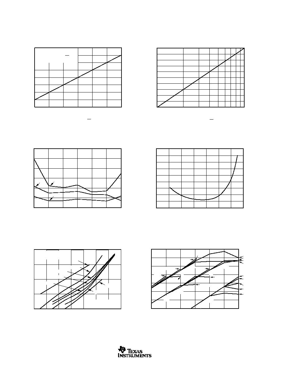
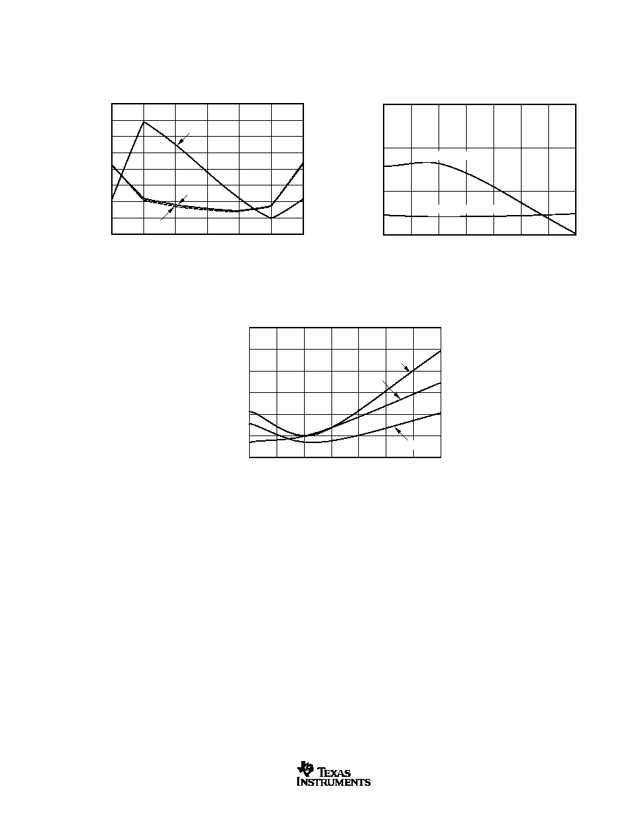
TYPICAL CHARACTERISTICS
At T
A
= +25
∞
C, V
S
=
±
5V, R
L
= 10k
, unless otherwise noted.
0
ONE CYCLE OF NORMALIZED TRANSFER FUNCTION
Normalized Output Voltage (V)
1
0.9
0.8
0.7
0.6
0.5
0.4
0.3
0.2
0.1
2
6
1
10
3
Current Ratio,
I
1
I
2
4
8
3dB FREQUENCY RESPONSE
I
2
3dB Frequency Response (Hz)
0.1
1nA
1M
100k
10k
1k
100
10
1
10nA
100nA
1
µ
A
10
µ
A
100
µ
A
1mA
100
µ
A
100
µ
A
1mA
I
1
= 1mA
1
µ
A
1mA
to 10
µ
A
100nA
10nA
I
1
= 1nA
10nA
10nA
1
µ
A
10
µ
A
100
µ
A
C
C
= 1
µ
F
C
C
= 1000pF
10
µ
A to 1
µ
A
C
C
= 10pF
I
1
= 1nA
1nA
100
µ
A
NORMALIZED TRANSFER FUNCTION
Normalized Output Voltage (V)
0.001
3
2
1
0
≠1
≠2
≠3
0.01
1
100
Current Ratio,
0.1
10
1000
I
1
I
2
I
1
I
2
V
OUT
= 1V ∑ Log
TOTAL ERROR vs INPUT CURRENT
Total Error (mV)
1nA
60
50
40
30
20
10
0
100nA
10nA
70
∞
C
0
∞
C
25
∞
C
10
µ
A
100
µ
A
Input Current
(I
1
or I
2
)
1
µ
A
1mA
MINIMUM VALUE OF COMPENSATION CAPACITOR
C
C
(pF)
1nA
10000
1000
100
10
1
100nA
10nA
10
µ
A
1mA
I
2
1
µ
A
100
µ
A
10mA
Select C
C
for I
1
min
and I
2
max
I
1
= 1nA
Values below 2pF
may be ignored.
I
1
= 1mA
I
1
= 100
µ
A
I
1
= 10nA
I
1
= 100nA
I
1
= 1
µ
A
I
1
= 10
µ
A
0.35
0.30
0.25
0.20
0.15
0.10
0.05
0.00
≠0.05
≠0.10
≠60
≠40
≠20
0
20
40
60
80
GAIN ERROR vs TEMPERATURE
Gain Error (%)
Temperature (
∞
C)
www.ti.com
LOG102
5
SBOS211A
TYPICAL CHARACTERISTICS
(Cont.)
At T
A
= +25
∞
C, V
S
=
±
5V, R
L
= 10k
, unless otherwise noted.
TOTAL ERROR vs TEMPERATURE
Total Error (mV)
0
60
50
40
30
20
10
0
30
10
20
50
60
Temperature (
∞
C)
40
70
1mA
1nA
10nA to 100
µ
A
LOG CONFORMITY vs V
LOGOUT
Log Conformity (mV)
≠3
5
4
3
2
1
0
≠1
≠2
≠3
≠1
≠2
1
2
V
LOGOUT
(V)
0
3
70
∞
C
0
∞
C
25
∞
C
LOG CONFORMITY vs TEMPERATURE
Log Conformity (m%)
0
300
200
100
0
30
10
20
50
60
Temperature (
∞
C)
40
70
6 Decades (1nA to 1mA)
5 Decades (1nA to 100
µ
A)