 | –≠–ª–µ–∫—Ç—Ä–æ–Ω–Ω—ã–π –∫–æ–º–ø–æ–Ω–µ–Ω—Ç: TDE1891 | –°–∫–∞—á–∞—Ç—å:  PDF PDF  ZIP ZIP |
TDE1890
TDE1891
2A HIGH-SIDE DRIVER
INDUSTRIAL INTELLIGENT POWER SWITCH
2A OUTPUT CURRENT
18V TO 35V SUPPLY VOLTAGE RANGE
INTERNAL CURRENT LIMITING
THERMAL SHUTDOWN
OPEN GROUND PROTECTION
INTERNAL NEGATIVE VOLTAGE CLAMPING
TO V
S
- 50V FOR FAST DEMAGNETIZATION
DIFFERENTIAL INPUTS WITH LARGE COM-
MON MODE RANGE AND THRESHOLD
HYSTERESIS
UNDERVOLTAGELOCKOUT WITH HYSTERESIS
OPEN LOAD DETECTION
TWO DIAGNOSTIC OUTPUTS
OUTPUT STATUS LED DRIVER
DESCRIPTION
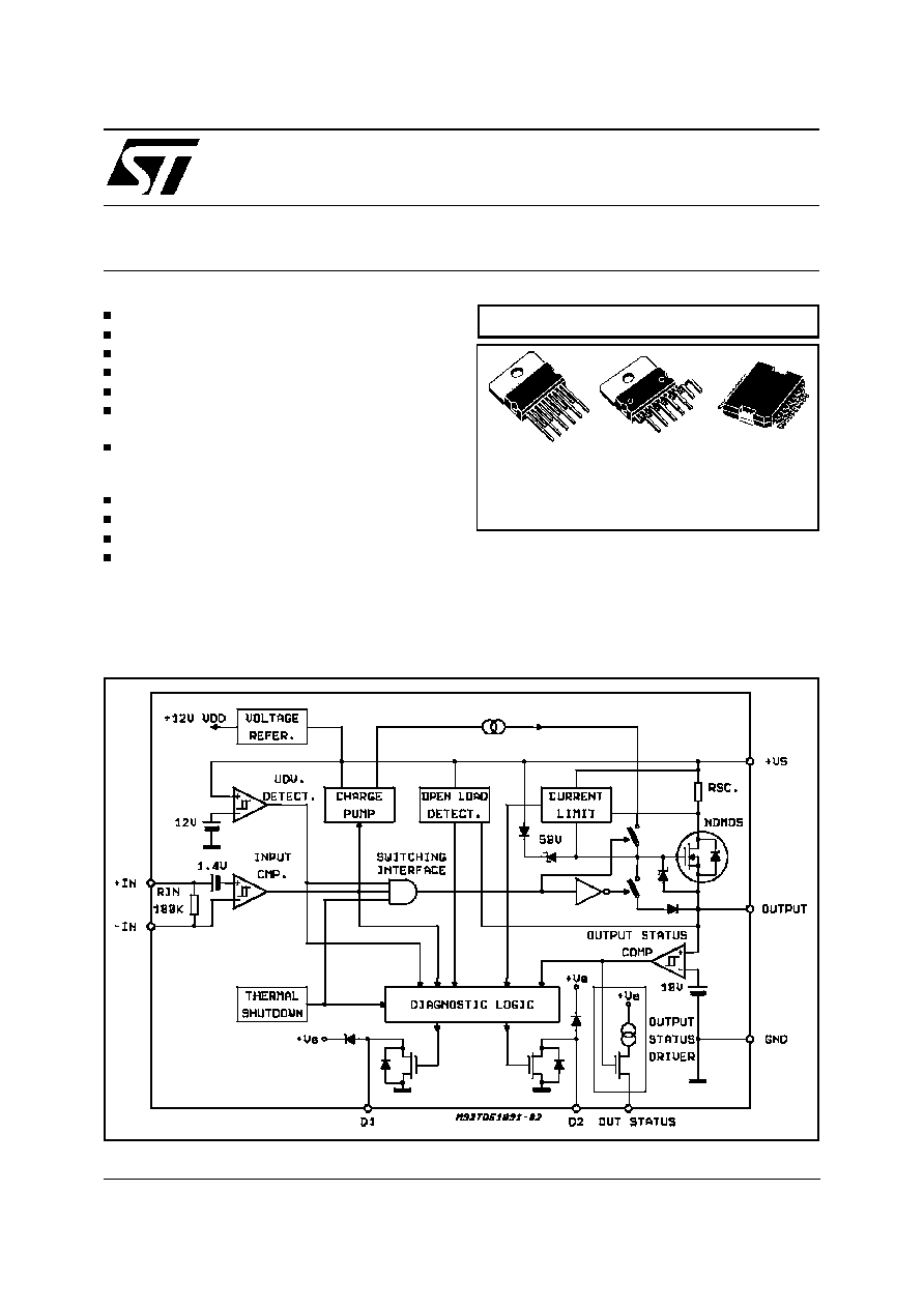
The TDE1890/1891 is a monolithic Intelligent
Power Switch in Multipower BCD Technology, for
driving inductive or resistive loads. An internal
Clamping Diode enables the fast demagnetization
of inductive loads.
Diagnostic for CPU feedback and extensive use
of electrical protections make this device ex-
tremely rugged and specially suitable for indus-
trial automation applications.
July 1998
Æ
MULTIWATT11 MULTIWATT11V
PowerSO20
(In line)
ORDERING NUMBERS:
TDE1891L
TDE1890V
TDE1890D
TDE1891V
BLOCK DIAGRAM
MULTIPOWER BCD TECHNOLOGY
1/12
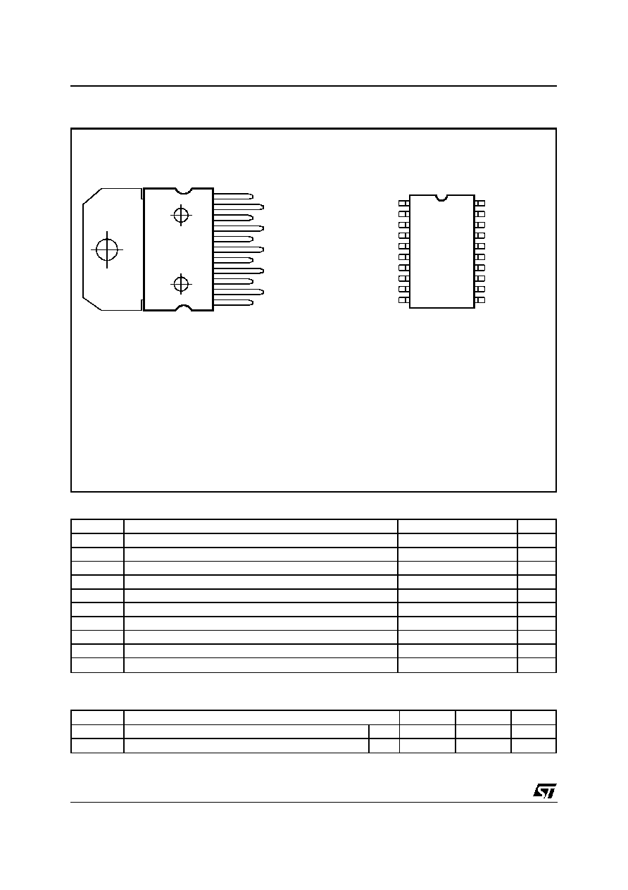
PIN CONNECTION (Top view)
ABSOLUTE MAXIMUM RATINGS
Symbol
Parameter
Value
Unit
V
S
Supply Voltage (Pin 10) (T
W
< 10ms)
50
V
V
S
≠ V
O
Supply to Output Differential Voltage. See also V
Cl
(Pins 10 - 9)
internally limited
V
V
i
Input Voltage (Pins 3/4)
-10 to V
S
+10
V
V
i
Differential Input Voltage (Pins 3 - 4)
43
V
I
i
Input Current (Pins 3/4)
20
mA
I
O
Output Current (Pin 9). See also ISC (Pin 9)
internally limited
A
P
tot
Power Dissipation. See also THERMAL CHARACTERISTICS.
internally limited
W
T
op
Operating Temperature Range (T
amb
)
-25 to +85
∞
C
T
stg
Storage Temperature
-55 to 150
∞
C
E
I
Energy Induct. Load T
J
= 85
∞
C
1
J
THERMAL DATA
Symbol
Description
Multiwatt
PowerSO20
Unit
R
th j-case
Thermal Resistance Junction-case
Max.
1.5
1.5
…C/W
R
th j-amb
Thermal Resistance Junction-ambient
Max.
35
≠
…C/W
1
2
3
4
5
6
7
9
10
11
8
OUTPUT
SUPPLY VOLTAGE
OUTPUT
N.C.
N.C.
GND
OUTPUT STATUS
INPUT -
INPUT +
DIAGNOSTIC 2
DIAGNOSTIC 1
D93IN022
GND
OUTPUT
OUTPUT
N.C.
SUPPLY VOLTAGE
N.C.
SUPPLY VOLTAGE
OUTPUT
OUTPUT
N.C.
N.C.
DIAGNOSTIC 1
N.C.
DIAGNOSTIC 2
INPUT +
INPUT -
OUTPUT STATUS
GND
1
3
2
4
5
6
7
8
9
18
17
16
15
14
12
13
11
19
10
20
GND
GND
D93IN021
Note: Output pins must be must be connected externally to the package to use all leads for the output current (Pin 9 and 11 for Multiwatt
package, Pin 2, 3, 8 and 9 for PowerSO20 package).
TDE1890 - TDE1891
2/12

ELECTRICAL CHARACTERISTICS (V
S
= 24V; T
amb
= ≠25 to +85
∞
C, unless otherwise specified)
Symbol
Parameter
Test Condition
Min.
Typ.
Max.
Unit
V
smin
Supply Voltage for Valid
Diagnostics
I
diag
> 0.5mA ; V
dg1
= 1.5V
9
35
V
V
s
Supply Voltage (operative)
18
24
35
V
I
q
Quiescent Current
I
ou t
= I
os
= 0
V
il
V
ih
3
5
7
8
mA
mA
V
sth1
Undervoltage Threshold 1
(See fig. 1), Tamb = 0 to +85
∞
C
11
V
V
sth2
Undervoltage Threshold 2
15.5
V
V
shys
Supply Voltage Hysteresis
1
V
I
sc
Short Circuit Current
V
S
= 18 to 35V; R
L
= 2
2.6
5
A
V
don
Output Voltage Drop
Iout = 2.0A T
j
= 25
∞
C
T
j
= 125
∞
C
I
out
= 2.5A T
j
= 25
∞
C
T
j
= 125
∞
C
360
575
440
700
500
800
575
920
mV
mV
mV
mV
I
oslk
Output Leakage Current
V
i
= V
il
; V
o
= 0V
500
µ
A
V
ol
Low State Out Voltage
V
i
= V
il
; R
L
=
0.8
1.5
V
V
cl
Internal Voltage Clamp (V
S
- V
O
)
I
O
= 1A
Single Pulsed: Tp = 300
µ
s
48
53
58
V
I
old
Open Load Detection Current
V
i
= V
ih
; T
amb
= 0 to +85
∞
C
0.5
9.5
mA
V
id
Common Mode Input Voltage
Range (Operative)
V
S
= 18 to 35V,
V
S
- V
id
< 37V
≠7
15
V
I
ib
Input Bias Current
V
i
= ≠7 to 15V; ≠In = 0V
≠250
250
µ
A
V
ith
Input Threshold Voltage
V+In > V≠In
0.8
1.4
2
V
V
iths
Input Threshold Hysteresis
Voltage
V+In > V≠In
50
400
mV
R
id
Diff. Input Resistance
0 < +In < +16V ; ≠In = 0V
≠7 < +In < 0V ; ≠In = 0V
400
150
K
K
I
ilk
Input Offset Current
V+In = V≠In
+Ii
0V < V
i
<5.5V
≠Ii
≠20
≠75
≠25
+20
µ
A
µ
A
≠In = GND
+Ii
0V < V+In <5.5V
≠Ii
≠250
+10
≠125
+50
µ
A
µ
A
+In = GND
+Ii
0V < V≠In <5.5V
≠Ii
≠100
≠50
≠30
≠15
µ
A
µ
A
V
oth1
Output Status Threshold 1
Voltage
(See fig. 1)
11.5
V
V
oth2
Output Status Threshold 2
Voltage
(See fig. 1)
8.5
V
V
ohys
Output Status Threshold
Hysteresis
(See fig. 1)
0.7
V
I
osd
Output Status Source Current
V
out
> V
oth1
; V
os
= 2.5V
2
4
mA
V
osd
Active Output Status Driver
Drop Voltage
VS ≠ V
os
; I
os
= 2mA
T
amb
= -25 to +85
∞
C
5
V
I
oslk
Output Status Driver Leakage
Current
V
out
< V
oth2
; V
os
= 0V
V
S
= 18 to 35V
25
µ
A
V
dgl
Diagnostic Drop Voltage
D1 / D2 = L ; I
diag
= 0.5mA
D1 / D2 = L ; I
diag
= 3mA
250
1.5
mV
V
I
dglk
Diagnostic Leakage Current
D1 / D2 =H ; 0 < Vdg < V
s
V
S
= 15.6 to 35V
25
µ
A
V
fdg
Clamping Diodes at the
Diagnostic Outputs.
Voltage Drop to V
S
Idiag = 5mA; D1 / D2 = H
2
V
Note V
il
< 0.8V, V
ih
> 2V @ (V+In > V≠In)
TDE1890 - TDE1891
3/12
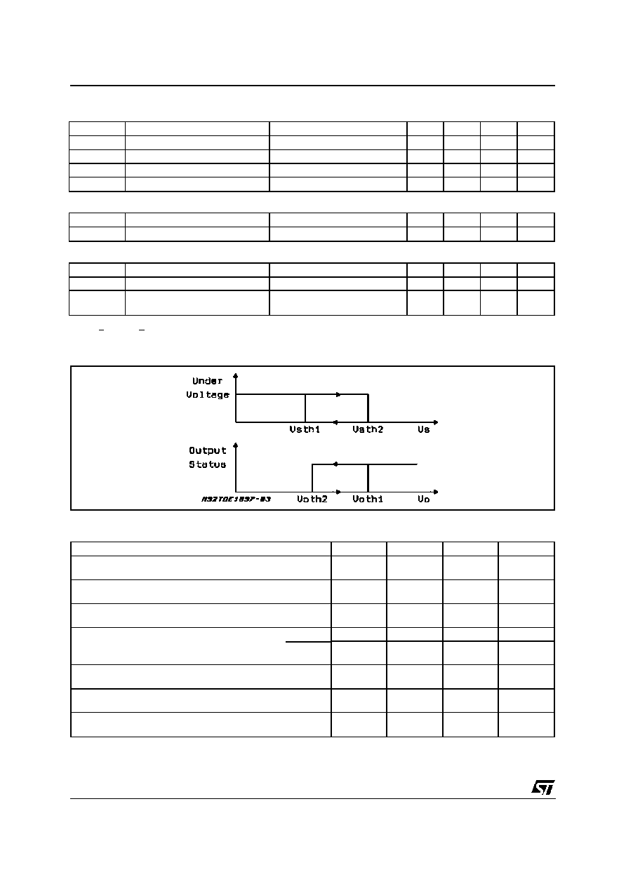
Figure 1
DIAGNOSTIC TRUTH TABLE
Diagnostic Conditions
Input
Output
Diag1
Diag2
Normal Operation
L
H
L
H
H
H
H
H
Open Load Condition (I
o
< I
old
)
L
H
L
H
H
L
H
H
Short to V
S
L
H
H
H
L
L
H
H
Short Circuit to Ground (I
O
= I
SC
)
(**)
TDE1891
TDE1890
H
<H (*)
H
L
H
H
L
H
H
H
H
Output DMOS Open
L
H
L
L
H
L
H
H
Overtemperature
L
H
L
L
H
H
L
L
Supply Undervoltage (V
S
< V
sth2
)
L
H
L
L
L
L
L
L
(*) According to the intervention of the current limiting block.
(**) A cold lamp filament, or a capacitive load may activate the current limiting circuit of the I PS, when the IPS is initially turned on. TDE1891
uses Diag2 to signal such condition, TDE1890 does not.
SOURCE DRAIN NDMOS DIODE
Symbol
Parameter
Test Condition
Min.
Typ.
Max.
Unit
V
fsd
Forward On Voltage
@ Ifsd = 2.5A
1
1.5
V
I
fp
Forward Peak Current
t = 10ms; d = 20%
6
A
t
rr
Reverse Recovery Time
If = 2.5A di/dt = 25A/
µ
s
200
ns
t
fr
Forward Recovery Time
100
ns
THERMAL CHARACTERISTICS
ÿ Lim
Junction Temp. Protect.
135
150
∞
C
T
H
Thermal Hysteresis
30
∞
C
SWITCHING CHARACTERISTICS (V
S
= 24V; R
L
= 12
)
t
on
Turn on Delay Time
200
µ
s
t
off
Turn off Delay Time
40
µ
s
t
d
Input Switching to Diagnostic
Valid
200
µ
s
Note Vil < 0.8V, Vih > 2V @ (V+In > V≠In)
TRUE
FALSE
HIGH
LOW
TDE1890 - TDE1891
4/12
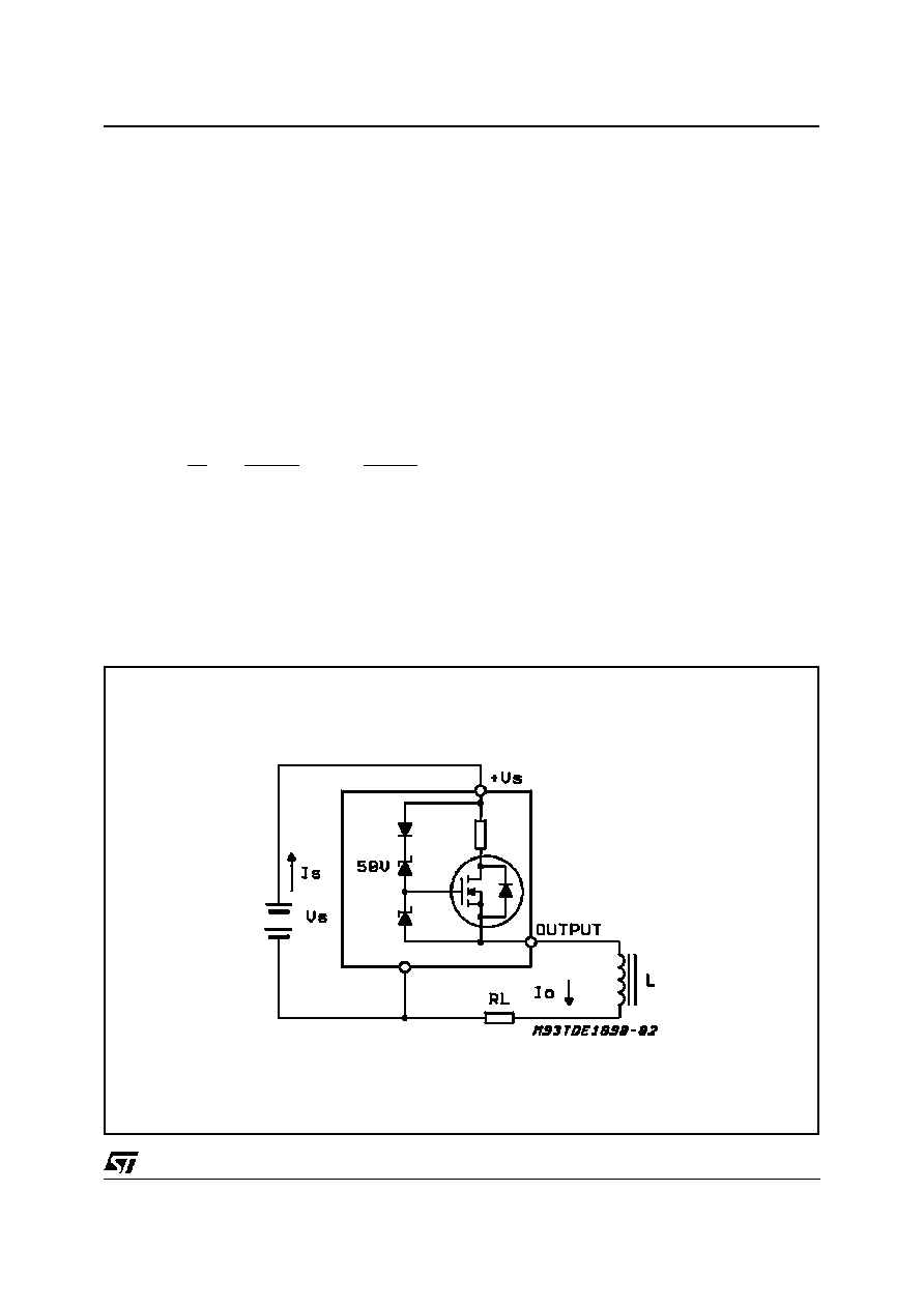
APPLICATION INFORMATION
DEMAGNETIZATION OF INDUCTIVE LOADS
An internal zener diode, limiting the voltage
across the Power MOS to between 50 and 60V
(V
cl
), provides safe and fast demagnetization of
inductive loads without external clamping devices.
The maximum energy that can be absorbed from
an
inductive
load
is
specified
as
1J
(at
T
j
= 85
∞
C).
To define the maximum switching frequency three
points have to be considered:
1) The total power dissipation is the sum of the
On State Power and of the Demagnetization
Energy multiplied by the frequency.
2) The total energy W dissipated in the device
during a demagnetization cycle (figg. 2, 3) is:
W
=
V
cl
L
R
L
[
I
o
≠
V
cl
≠ V
s
R
L
log
1
+
V
s
V
cl
≠ V
s
]
Where:
V
cl
= clamp voltage;
L = inductive load;
R
L
= resistive load;
Vs = supply voltage;
I
O
= I
LOAD
3)
In normal conditions the operating Junction
temperature should remain below 125
∞
C.
If the demagnetization energy exceeds the rated
value, an external clamp between output and +V
S
must be externally connected (see fig. 5).
The external zener will be chosen with V
zener
value lower than the internal V
cl
minimum rated
value and significantly (at least 10V) higher than
the voltage that is externally supplied to pin 10,
i.e. than the supply voltage.
Alternative circuit solutions can be implemented
to divert the demagnetization stress from the
TDE1890/1, if it exceeds 1J. In all cases it is rec-
ommended that at least 10V are available to de-
magnetize the load in the turn-off phase.
A clamping circuit connected between ground and
the output pin is not recommended. An interrup-
tion of the connection between the ground of the
load and the ground of the TDE1890/1 would
leave the TDE1890/1 alone to absorb the full
amount of the demagnetization energy.
Figure 2: Inductive Load Equivalent Circuit
TDE1890 - TDE1891
5/12