TDE0160
April 1993
PROXIMITY DETECTOR
.
SUPPLY VOLTAGE : +4 TO +36V
.
SUPPLY CURRENT : < 1.2mA
.
OUTPUT TRANSISTORS : I = 20mA ;
V
CE
(
sat
)
1100mV
.
OSCILLATOR FREQUENCY : < 1MHz
.
LOSS RESISTANCE : 5 TO 50k
.
DESCRIPTION
The TDE0160 is designed to detect metal bodies
by the effect of Eddy currents on the HF losses of
a coil. It has two complementary open collector
outputs with peak limiting. Hysteresis is adjustable,
and an electronic switching circuit is incorporated
for disabling both outputs.
An internal zener diode maintains the supply volt-
age to the circuit in "dipole" operation.
PIN CONNECTION (top view)
DIP14
ORDERING NUMBERS : TDE0160DP (DIP14)
TDE 0160FP (SO14)
SO14
1/8

ABSOLUTE MAXIMUM RATINGS
Symbol
Parameter
Value
Unit
V
CC
Supply Voltage
36
V
V
O*
Output Voltage*
36
V
I
O
(I
1
-I
3
)
Output Current (I
1
-I
3
)
40
mA
I
Z
Zener Current
40
mA
T
j
Junction Temperature
+ 150
∞
C
T
oper
Ambient Temperature Range
≠ 25 to + 85
∞
C
T
stg
Storage Temperature Range
≠ 65 to + 150
∞
C
* Internal peak limiting to protect against transient voltage surges.
SCHEMATIC DIAGRAM
TDE0160
2/8

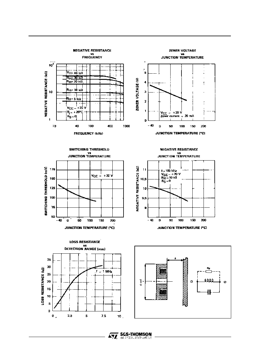
ELECTRICAL CHARACTERISTICS
T
amb
= +25
o
C unless otherwise specified
Symbol
Parameter
Min.
Typ.
Max.
Unit
V
CC
Supply Voltage
Pin 11
4
36
V
V
Z
Zener Voltage (I
Z
= 20mA)
Pins 9-11
3
4
V
I
CC
Supply Current
Pin 11
1.2
mA
≠
Limiting (I = 0.1mA)
Pin 1 or 3
42
V
≠
Output Transistor Saturation Voltage
Pin 1 or 3
(I
1
or I
3
= +20mA)
0.9
1.1
V
≠
Output Transistor Leakage Current (V = +30V)
Pin 1 or 3
2
µ
A
≠
Switching Threshold
Pin 12
90
110
130
mV
R
n
Negative Resistance*
(5k
< R
H
< 50k
, f = 100kHz, R
S
= 0)
R
n
= R
H
≠
Inherent Hysteresis (R
2
= 0)
1
2
%
≠
Programmed Hysteresis (H < 15%)
R
s
R
s
+
R
H
%
f
osc
Oscillation Frequency
1
MHz
≠
Switching Frequency (with matched oscillator circuit)
750
Hz
≠
Switching Time-delay
0.5 C
d
(
µ
F)
s
≠
Switching Response Time (C
d
= 10nF ; V
CC
= +20V)
10
µ
s
* See characteristic curves
SWITCHING OPERATION
If I
C
exceeds I
CO
, where I
CO
=
V
(
ref
)
R
d
the switch
cuts off the output transistors and tests the value
of current I
C
, with time constant 0.5 C
d
.
On power up the internal start system cuts off the
output transistors until V
CC
reaches a value permit-
ting normal operation of the circuit.
TDE0160
3/8