 | –≠–ª–µ–∫—Ç—Ä–æ–Ω–Ω—ã–π –∫–æ–º–ø–æ–Ω–µ–Ω—Ç: STLC5445 | –°–∫–∞—á–∞—Ç—å:  PDF PDF  ZIP ZIP |

1/23
STLC5445
October 2002
s
BATTERY VOLTAGE UP TO 120V
s
SUPPLIES POWER FOR UP TO FOUR
DIGITAL TELEPHONE LINES
s
PROGRAMMABLE CURRENT LIMITING
s
LONGITUDINAL CURRENT CANCELLATION
s
ETSI ETR80 COMPLIANT
s
OUTPUT CURRENT UP TO 140 mA
s
STATUS CONDITION DETECTION FOR
EACH LINE
s
AUTOMATIC THERMAL PROTECTION
s
AUTO POWER ON SEQUENCE
s
OUTPUT STAGE OPTIMIZED FOR MINIMAL
OUTPUT OVERVOLTAGE PROTECTION
s
TWO EXTERNAL RELAY DRIVERS PER LINE
s
PARALLEL OR MPI CONTROL INTERFACE
s
HI-QUAD PACKAGE 64 PIN
DESCRIPTION
The QUAD LINE FEED CONTROLLER provides a
power source for up to four U line interfaces. The
power source to the device is a local battery or a cen-
tralized regulated power supply. Each powered line is
individually controlled and monitored by the device
interface.
A MPI or a simple parallel interface can be selected
by a pin strap.
Each line can be individually powered and monitored:
therefore overload and faults can easily be detected
and localized even in a large system. The status con-
ditions detected by the device are: Current Overload,
Thermal Overload, Open Loop. If activated (by
means of a dedicated pin strap), a self generated
power on sequence avoids the thermal over stress
when a simultaneous power on has been requested
for more than one channel. The current limiting value
can globally be programmed for the four channels by
means of an external resistor. The device has two in-
tegrated relay drivers per line to drive the test relays
of the ISDN system.
HiQUAD-64
ORDERING NUMBER: STLC5445
QUAD LINE FEED CONTROLLER

STLC5445
2/23
BLOCK DIAGRAM
Relay driver 3B
Relay driver 3A
Relay driver 2B
Relay driver 2A
Relay driver 1B
VCC
WA0
CODC0
WB0
WBP0
Channel 3
Channel 2
Channel 1
V
BAT
On / Off
&
line current
control
OLD
COD
Channel 0
COD & OLD
generation
Logic
interface
ILIM
PSC
PBIT
CKILC
RESETN
INTN
ALE
ES0 (A0)
ES1 (CSN)
ES2 (RDN)
ES3 (WRN)
NACK0 (D0)
NACK1 (D1)
NACK2 (D2)
NACK3 (D3)
Reference & biasing
generation
Thermal
monitoring
110∞C
130∞C
160∞C
Voltage
and
current
biasing
Relay driver 1A
Relay driver 0B
Relay driver 0A
EREL0B
REL0A
REL0B
REL1A
REL1B
REL2A
REL2B
REL3A
REL3B
EREL0A
EREL1A
EREL1B
EREL2A
EREL2B
EREL3A
EREL3B
VCC
BGND
DGND
RGND
VBAT
VBAT
Driving
&
output
clamping
I / O connections on channels 1, 2 and
3 are similar to those
shown for channel 0 but have been omitted for clarity
reasons.
Limiting
current
reference

3/23
STLC5445
PIN CONNECTION (Top view)
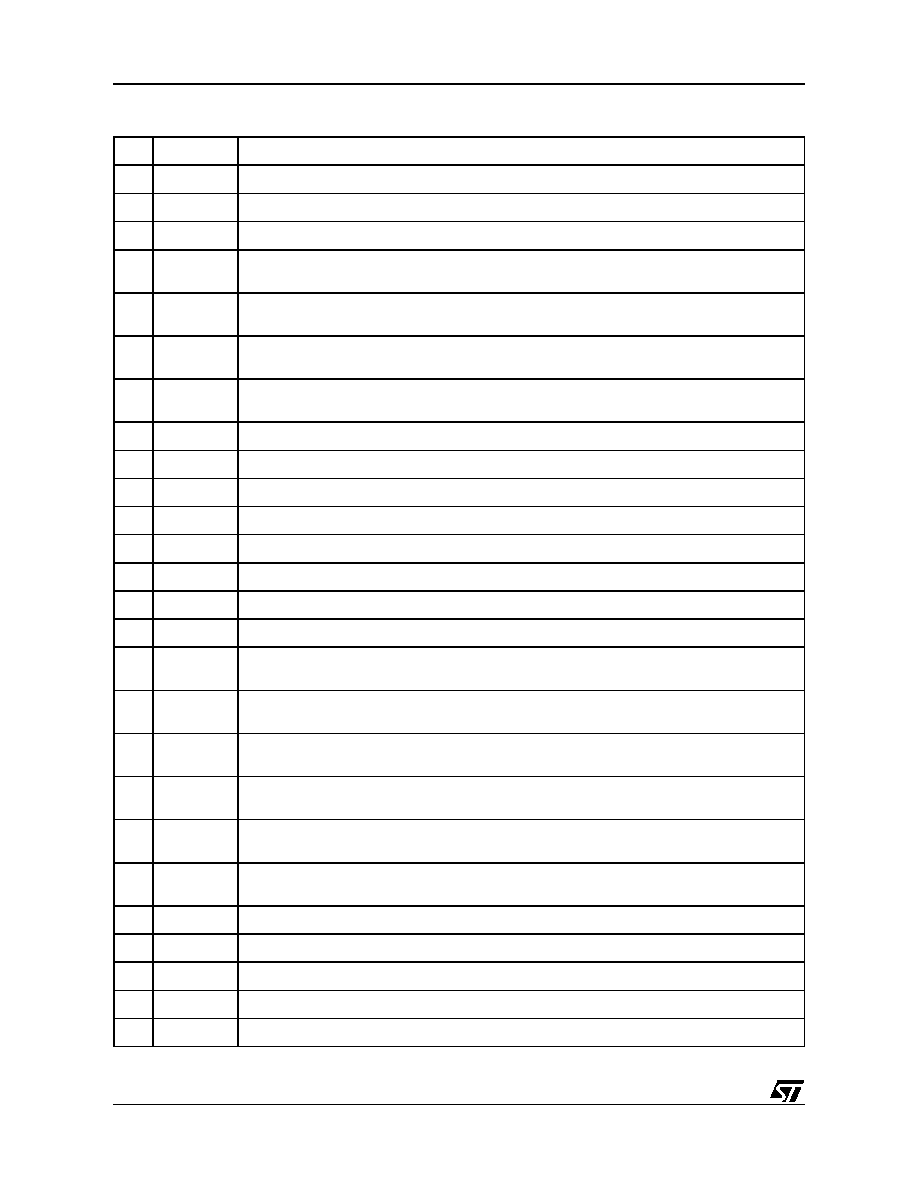
PIN FUNCTION
N∞
Pin Name
Description
1
CODC0
Pin for connection of the external capacitor (100nF/6.3V) to GND for COD signal filtering on
channel 0.
2
CODC1
Pin for connection of the external capacitor (100nF/6.3V) to GND for COD signal filtering on
channel 1
4
CKILC
External clock input pin for the internal power on sequencer
5
NACK0(D0)
Logic pin: with PSC = 0, Line 0 status information output
with PSC = 1, Line 0 I/O tristate data bus
6
NACK1(D1)
Logic pin: with PSC = 0, Line 1 status information output
with PSC = 1, Line 1 I/O tristate data bus
7
REL0A
Output of the 0A relay driver
8
*EREL0A
Logic input pin: relay 0A output driver's ON/OFF (high = ON)
9
*EREL0B
Logic input pin: relay 0B output driver's ON/OFF (high = ON)
10
REL0B
Output of the 0B relay driver
11
REL1A
Output of the 1A relay driver
1
2
3
5
6
4
7
8
9
10
27
11
28 29 30 31 32
59
58 57 56 55 54 53
47
46
45
43
42
44
52
51
50
48
49
NACK1(D1)
NACK0(D0)
CK_ILC
CODC1
CODC0
RGND
REL1A
REL0B
*EREL0B
REL0A
*EREL0A
VBAT
VBAT
WB2
WBP2
DGND
WA2
BGND
VBAT
VBAT
WB3
WBP3
ILIM
N.C.
WA3
NACK2(D2)
REL3B
*EREL3B
REL3A
REL2B
*EREL3A
N.C.
BGND
NACK3(D3)
*RESET
D99TL437
26
60
WB0
61
WBP0
62
RGND
63
WA0
64
BGND
WA1
N.C.
V
CC
WBP1
WB1
21 22 23 24 25
41
40
38
37
39
*EREL2B
*EREL2A
*ES2(RD)
*ES1(CS)
*ES3(WR)
12
13
14
15
16
PBIT
ALE
REL1B
*EREL1A
*EREL1B
36
34
33
35
*ES0(A0)
CODC3
CODC2
RGND
17
18
19
20
N.C.
BGND
INTN
PSC
REL2A
*INTERNAL PULL DOWN TO GROUND
STLC5445
4/23
12
*EREL1A
Logic input pin: relay 1A output driver's ON/OFF (high = ON)
13
*EREL1B
Logic input pin: relay 1B output driver's ON/OFF (high = ON)
14
REL1B
Output of the 1B relay driver
15
ALE
Logic input pin: with PSC = 0, Don't care
with PSC = 1, Address Latch Enable (active high)
16
PBIT
Power on sequencer enable: PBIT = 0: power on sequencer ON
PBIT = 1: power on sequencer OFF
17
PSC
Parallel or MPI mode input selection pin:
0 = parallel interface; 1 = MPI interface
18
INTN
Logic output pin; open drain: with PSC = 0 high impedance
with PSC = 1 interrupt (active low)
21
WA1
Output feeder's switch side of line 1; negative respect to WB1
23
VCC
Positive supply voltage. It is referred to DGND
24
WBP1
Internal protection diodes for line 1
25
WB1
Output feeder's resistive side of line 1; positive respect to WA1
28
WB2
Output feeder's resistive side of line 2; positive respect to WA2
29
WBP2
Internal protection diodes for line 2
30
DGND
Digital ground
31
WA2
Output feeder's switch side of line 2; negative respect to WB2
33
CODC2
Pin for connection of the external capacitor (100nF/6.3V) to GND for COD signal filtering on
channel 2
34
CODC3
Pin for connection of the external capacitor (100nF/6.3V) to GND for COD signal filtering on
channel 3
36
*ES0(A0)
Logic input pin: with PSC = 0, Line 0 ON/OFF request (high=ON)
with PSC = 1, Address bit for R/W operations
37
*ES1(CSN)
Logic input pin: with PSC = 0, Line 1 ON/OFF request (high=ON)
with PSC = 1, chip select (active low)
38
*ES2(RDN)
Logic input pin: with PSC = 0, Line 2 ON/OFF request (high=ON)
with PSC = 1, Read command (active low)
39
*ES3(WRN)
Logic input pin: with PSC = 0, Line 3 ON/OFF request (high=ON)
with PSC = 1, Write command (active low)
40
REL2A
Output of the 2A relay driver
41
*EREL2A
Logic input pin: relay 2A output driver's ON/OFF (high = ON)
42
*ERL2B
Logic input pin: relay 2B output driver's ON/OFF (high = ON)
43
REL2B
Output of the 2B relay driver
44
REL3A
Output of the 3A relay driver
N∞
Pin Name
Description
PIN FUNCTION (continued)

5/23
STLC5445
* Internal pull down to ground
45
*EREL3A
Logic input pin: relay 3A output driver's ON/OFF (high = ON)
46
*ERL3B
Logic input pin: relay 3B output driver's ON/OFF (high = ON)
47
REL3B
Output of the 3B relay driver
48
NACK2 (D2) Logic pin: with PSC = 0, Line 2 status information output
with PSC = 1, Line 2 I/O tristate data bus
49
NACK3 (D3) Logic pin: with PSC = 0 line 3 status information output
with PSC = 1 line 3 I/O tristate data bus
50
*RESETN
Logic input pin: reset (active low)
53
WA3
Output feeder's switch side of line 3; negative respect toWB3
55
ILIM
Current limit programming input
56
WBP3
Internal protection diodes for line 3
57
WB3
Output feeder's resistive side of line 3; positive respect to WA3
60
WB0
Output feeder's resistive side of line 0; positive respect to WA0
61
WBP0
Internal protection diodes for line 0
0
WA0
Output feeder's switch side of line 0; negative respect to WB0
26
27
58
59
VBAT
Negative battery supply voltage. It is referred to BGND
19
32
51
64
BGND
Battery ground
3
35
62
RGND
Relay ground
N∞
Pin Name
Description
PIN FUNCTION (continued)