
March 1996
This is advance information on a new product now in development or undergoing evaluation. Details are subject to change without no tice.
PLCC68
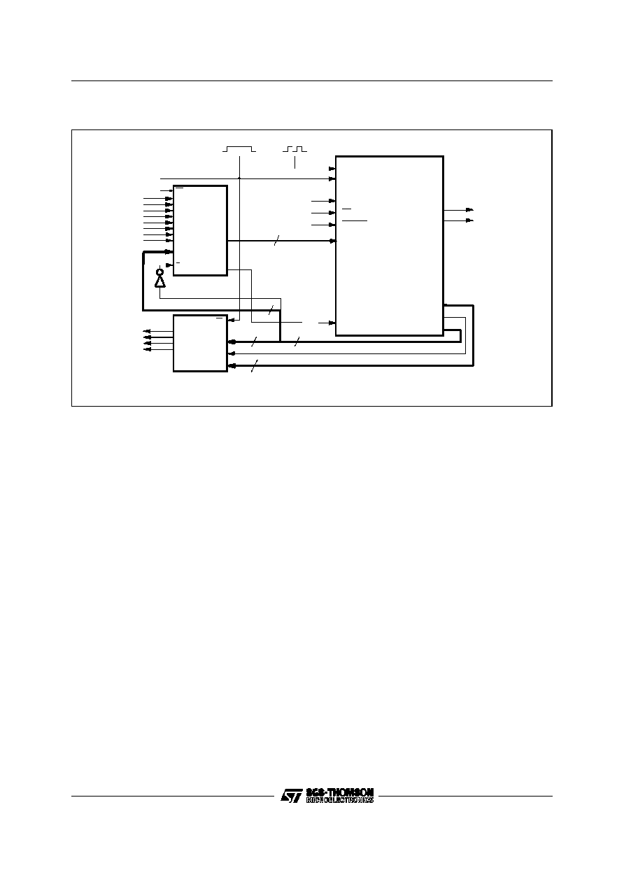
8
I0-I7
BUSY
OFL
12
O0-O1 1
2
OC0-OC1
DS
PRESET
VSS
VDD
W.A.R. P.
2.0
LASTIN
MCLK
WAIT
ENDOFL
ERR
O E
AUTO
3
SIS0- SI S2
RD
READY
Figure 1. Logic Diagram.
Digital Fuzzy Co-processor 8-bit I/O
High Speed Rules Processing
4 Input, 2 Output, 32 Rules in 33.1
µ
s
Up to 256 Rules (4 Antecedents,1 Consequent)
Up to 8 Input Configurable Variables
Up to 16 Membership Functions for an Input
Variable
Antecedent Membership Functions with
Triangular and Trapezoidal Shape
Up to 4 Output Variables
Up to 256 Membership Functions for all
Consequents
Singleton Consequent Membership Functions
Defuzzification on chip
Maximum Clock Frequency 40MHz
A/D Start Convertion Pulse presettable
Direct Interface to all popular microprocessor
Handshaking Signal Polarity presettable
Operates "STAND ALONE" (without
µ
P) if
desired
Standard +5V Supply Voltage
Software Tools and Emulators Availability
Pin number: 52
68-lead Plastic Leaded Chip Carrier package.
ANTECE DENT
MEMORY
P ROGRAM &
CONSE QUENT
MEMORY
P ROGRAMMABLEA/D
OUTPUT PULSE
INTERNAL BUS
Input Port
with
HANDSHAKE
8
ALPHA
CALCULATOR
INFE RENCE
UNIT
DEFUZZIFIER
Ouput Port
with
HANDSHAKE
8
Figure 2. Simplified Block Diagram.
W.A.R.P.2.0
8-BIT FUZZY CO-PROCESSOR
PRELIMINARY DATA
1/28

GENERAL DESCRIPTION
W.A.R.P.2.0 is a member of the W.A.R.P. family of
fuzzy microprocessors, completely developed and
produced by SGS-THOMSON Microelectronics us-
ing the high performance, reliable HCMOS4T
(O.7
µ
m) process.
W.A.R.P.2.0 can be used both as a Fuzzy Co-proc-
essor or as a stand-alone microcontroller. In the
former case, it can work together with standard
micros which shall perform normal control tasks
while W.A.R.P.2.0 will be indipendentlyresponsible
for all the fuzzy related computing.
W.A.R.P.2.0 core includes the fuzzifier (ALPHA
calculator), the inference unit, and the defuzzifier.
The I/O capabilities demanded by microprocessor
applications are fulfilled by W.A.R.P.2.0 with 8 Input
and 4 Output lines which can be supported by
handshaking signals.
The capability of preset the polarity of the hand-
shaking signals simplifies the interface with the
host processor.
An internal Start Conversion pulse is provided to
allow simple use for waveform generation which
can be directly applied to drive an A/D converter.
The output 3-STATE buffer can be temporarily
frozen in order to synchronize W.A.R.P.2.0 with
slower devices.
9
8
7
6
5 4 3
2
1 68 67 66 65 64 63 62 61
27 28 29 30 31 32 33 34 35 36 37 38 39 40 41 42 43
16
15
14
13
12
11
10
44
45
46
47
48
49
50
51
52
53
54
55
56
57
58
59
60
W.A.R.P. 2.0
nc
nc
nc
VDD
VSS
O0
O1
O2
O3
O4
O5
O6
VDD
VSS
nc
nc
nc
VSS
VDD
MCLK
PRESET
OFL
AUTO
LASTIN
OE
RD
TEST
DS
ENDOFL
ERR
BUSY
READY
VSS
VDD
nc
nc
I7
I6
I5
I4
I3
I2
VSS
I1
I0
WAIT
SIS0
SIS1
SIS2
nc
nc
nc
nc
nc
VSS
VDD
OC1
OC0
O11
O10
O9
O8
O7
VSS
VDD
nc
nc
nc
26
25
24
23
22
21
20
19
18
17
Figure 3. Pin Connections
Running W.A.R.P.2.0 involves a downloading
phase and an On-Line phase. The downloading
phase allows the setting of the processor, in terms
of I/O number, universe of discourse, Membership
Functions (MFs) and rules. During this phase
W.A.R.P.2.0 prepares its internal memories for the
On-Line elaboration phase and loads the micro-
code in its program memory. This microcode, which
drives the On-Line phase, is generated by the
Compiler (see FUZZYSTUDIO
TM
2.0 User Man-
ual). After that W.A.R.P.2.0 is ready to run (On-Line
phase) processing inputs and producing the re-
lated outputs according to the configuration loaded
in the downloading phase. It is also possible to
provide the processor with inputs in any order by
specifying their identification numbers.
Two basic memories are available in W.A.R.P.2.0 :
the Antecedent Memory (AM) and the Pro-
gram/Consequent Memory (PCM). The antece-
dent MFs, portrayed by a resolution of 2
8
elements,
are stored in the AM (256 bytes). W.A.R.P.2.0
exploits a SGS-THOMSON patented strategy to
store the MFs in the AM.
The information about Rules and Consequent MFs
are stored in the PCM (1.4 Kbyte).
FUZZYSTUDIO
TM
2.0 is a powerful development
environment consisting of board and software al-
lows an easy configuration and use of W.A.R.P.2.0.
Note: nc = Not Connected.
2/28
W.A.R.P.2.0

Pin Assignment
Name
Pins Type
Fun ction
11,26,31,40,48,57
VDD
-
Power Supply
1,10,25,30,39,47,56
VSS
-
Ground
19
TEST
I
Testing (It must be connected to VSS)
12
MCLK
I
Master Clock (up to 40 MHz)
13
PRESET
I
Preset
15
AUTO
I
Auto/Manual-Boot
65
SIS0
I
Auto-Boot Speed (Ext. Memory Support AccessTime) /
Input Selection bit 0
64
SIS1
I
Auto-Boot Speed (Ext. Memory Support Access Time) /
Input Selection bit 1
63
SIS2
I
Auto-Boot Speed (Ext. Memory Support Access Time) /
Input Selection bit 2
67
I0
I
Data Input bit 0
68
I1
I
Data Input bit 1
2
I2
I
Data Input bit 2
3
I3
I
Data Input bit 3
4
I4
I
Data Input bit 4
5
I5
I
Data Input bit 5
6
I6
I
Data Input bit 6
7
I7
I
Data Input bit 7
14
OFL
I
Off-Line/On-Line Switch
18
RD
I
Handshaking Read Ready
16
LASTIN
I
Last Input (Start Elaboration) bit
17
OE
I
Output Enable/3-STATE bit
66
WAIT
I
Temporary Output Processing Stop
24
READY
O
Handshaking Output Signal
21
ENDOFL
O
Offline Phase (external memory downloading) End
23
BUSY
O
Elaboration Phase Indicator
20
DS
O
Data Strobe (Output Ready Signal)
22
ERR
O
Error Flag
33
OC0
O
Output Identifier bit 0
32
OC1
O
Output Identifier bit 1
55
O0
O
External Memory Address/Defuzzified Output bit 0
54
O1
O
External Memory Address/Defuzzified Output bit 1
53
O2
O
External Memory Address/Defuzzified Output bit 2
52
O3
O
External Memory Address/Defuzzified Output bit 3
51
O4
O
External Memory Address/Defuzzified Output bit 4
50
O5
O
External Memory Address/Defuzzified Output bit 5
49
O6
O
External Memory Address/Defuzzified Output bit 6
38
O7
O
External Memory Address/Defuzzified Output bit 7
37
O8
O
External Memory Address bit 8 /
Next Input Progressive Number bit 0
36
O9
O
External Memory Address bit 9 /
Next Input Progressive Number bit 1
35
O10
O
External Memory Address bit 10 /
Next Input Progressive Number bit 2
34
O11
O
External Memory Address bit 11 /
Start Conversion for the external A/D
Table 1. Pin Description
3/28
W.A.R.P.2.0

PIN DESCRIPTION
Signals READY, RD, WAIT, DS, BUSY, LASTIN
and O11 ( external A/D Start Conversion) have
programmable polarity, see table 6 for default
values.
V
DD
, V
SS
. Power is supplied to W.A.R.P. using
these pins. V
DD
is the power connection and V
SS
is
the ground connection; multi-connections are nec-
essary.
MCLK.
Master Clock (Input): This is the input
master clock whose frequency can reach up to
40MHz (MAX).
During the Off-Line phase with AUTO High, the
MCLK is internally divided to utilize boot memories
working with a slower frequency.The access speed
is presettable by means of SIS0-SIS2 pins.
PRESET.
Preset (Input, active Low) : This is the
restart pin of W.A.R.P.. It is possible to restart the
work during the computation (On-Line phase) or
before the writing of internal memories (Off-Line
phase). In both cases it must be put Low at least
for a clock period. After PRESET Low the proces-
sor remains in the reset status 3 MCLK pulses.
AUTO.
Auto-Boot: (Input, active High): During the
Off-Line phase AUTO High enables the automatic
boot of W.A.R.P.2.0 whereas AUTO Low validates
the manual downloading. The manual boot has to
be performed using the handshaking signals
RD/READY.
During the On-Line phase AUTO High disables
the generation of the Start A/D conversion (O11)
signal.
SIS0-SIS2.
Speed & Input Selection (Inputs): Dur-
ing the Off-Line phase with AUTO High (Auto-Boot)
SIS bus allows to choose the speed of downloading
from the external memory which contains the start-
up configuration of W.A.R.P.2.0. In that case (Auto-
Boot) MCLK is internally divided to provide a slower
sinchronization signal which is automatically used
as RD for the reading of the external memory. Table
2 shows how to preset the frequency of this syn-
chronization signal.
During the On-Line phase in Slave mode (see
Register Bench description, Tab.5) SIS bus allows
to provide W.A.R.P.2.0 with inputs in any order by
specifying their identification number. The input
and its identification number (SIS0-SIS2) will be
acquired at the next active RD so they must be
already stable when RD is given.
SIS0
SIS1
SIS2
Internal Synchronization
Signal Frequency
Low
Low
Low
MCLK/32
High
Low
Low
MCLK/16
Table 2. Downloading Speed
I0-I7.
Input bus (Input): During the Off-Line phase
these 8 data input pins accept addresses and data
from the external boot memory containing
W.A.R.P.2.0 configuration. This start-up memory
(which can be a ZERO-POWER, the host proces-
sor memory, an EPROM, a Flash, the PC Memory,
etc.) contains the fuzzy project built by means of
FUZZYSTUDIO
TM
2.0.
In On-Line mode this bus carries the input variables
according to the prefixed order.
OFL.
Offline (Input, active High): When this pin is
High, the chip is enabled to load data in the internal
RAMs (Off-Line phase). It must be Low when the
fuzzy controller is waiting for input values and
during the processing phase (On-Line phase).
When OFL changes its status the processor re-
mains presetted for 3 clock pulses.
LASTIN.
Last Input (Input, default active High):
During the On-Line phase in slave mode (see
Register Bench description, table 5) LASTIN High
indicates no other inputs have to be provided so
W.A.R.P.2.0 can start the processing phase.
W.A.R.P.2.0 inputs are those in the input interface
so if some variables do not need to be acquired
again (because they change slower than others)
they remain stored and no extra time is required to
acquire them again.
OE.
Output Enable (Input, active Low): OE Low
enables O0-011output bus or (if High) put it in
3-STATE.
WAIT.
Wait (Input, default active High): This pin
High stops the output processing. When WAIT is
enabled W.A.R.P.2.0 finishes to compute the cur-
rent output variable but it does not give it on the
output bus until WAIT becomes Low. This signal
allows to synchronize W.A.R.P.2.0 with slower de-
vices.
RD.
Read
(Input, default active High): Both in
Off-Line and in On-Line mode RD indicates data
are ready to be acquired from the input bus I0-I7.
READY.
Ready (Output, default active High): Both
in Off-Line and in On-Line mode RD indicates data
have been acquired from the input bus I0-I7 and
are now stored in W.A.R.P.2.0 internal registers.
ENDOFL.
End of Off-Line phase (Output, active
High): This pin indicates the end of the download-
ing phase (Off-Line) so the content of the boot
memory is already stored in W.A.R.P.2.0 internal
memories. After ENDOFL is active the user can put
OFL Low so the On-Line phase can start.
BUSY.
Busy Signal (Output, default active High):
When the elaboration phase is running this pin is
active. When W.A.R.P.2.0 finishes to compute the
last output variable, it puts BUSY Low and waits
for new inputs.
4/28
W.A.R.P.2.0

DS.
Data Strobe (Output, default active High): The
strobe pin enables the user to utilize the output.
When this pin is High it indicates that a new output
variable has been calculated and it is ready on the
output bus (O0-O7). This signal synchronizes the
external devices and in particular the interfaces
with the controlled processes (On-Line mode).
ERR.
Error (Output, active Low): When this pin is
active, W.A.R.P.2.0 has incurred in an internal error
condition.
OC0-OC1.
Output Counter (Output): This 2 bit
output bus provides the output variables with a
progressive number during the On-Line phase. As
a consequence it is possible to know to which
variable correspond the data that are on the output
data bus (O0-O7). The dimension of OC bus is
connected with the maximum number of output
variables (4).
O0-O11.
Output Bus
(Output): In the Off-Line
phase these pins provide the addresses (12 bit) for
its internal memories and send those addresses to
the external memory support where data to load are
located. These addresses sent on O0-O11 bus
allow to identify the data that have to be loaded in
W.A.R.P.2.0 internal memories.
In the On-Line phase O0-O7 carrie out the outpu t
values. When the DS is High, one output variable
can be read by external devices. The resolution
of output variables is 256 points (8 bit). If there is
more than one output, the output variables are
calculated one by one and they are provided in
the sequence stabilized during the editing phase
(see FUZZYSTUDIO
TM
2.0 User Manual).
In On-Line mode O8-O10 provide the progressive
number of the next variable to be acquired. These
pins can be used to select the next input to provide
on I0-I7 bus.
Still in on-line mode O11 allows to provide a preset-
table signal which can be used as Start-Conversion
for an A/D converter after (about 400 ns) OFL or
BUSY fall.
5/28
W.A.R.P.2.0

FUNCTIONAL DESCRIPTION
W.A.R.P.2.0 works in two mode depending on the
OFL control signal level (see table 3) :
Off-line MODE (OFL High)
On-line MODE (OFL Low)
OFF-LINE MODE
All W.A.R.P. memories are loaded during the Off-
Line phase. The membership functions are written
inside their related memories and the process con-
trol rules are loaded inside the PCM.
The addresses of the words to be written in the
memories, are internally generated while the ad-
dresses of the external memory locations to be
read are directly provided by W.A.R.P.2.0 by means
of O0-O11 output pins.
Data must be loaded 8 bit a time in the data bus
and can be read from an external non volatile
memory or loaded by an host processor.
The Off-Line phase can be performed automat-
ically (see figure 4) or manually (see figure 5).
When the auto-boot is chosen (AUTO = High) it is
possible to configure the reading access time of the
external memory. The auto-boot end is indicated by
the ENDOFL signal.
The downloading phase requires:
F*NWordsDatabase clock pulses,
where F is 16 or 32 (see table 2).
NWordsDatabase is the number of words stored in
the boot-memory (see register bench description,
table 5).
When the manual-boot is chosen (AUTO = Low)
data have to be provided by using the handshaking
signals (RD/READY). In this way it is possible to
update only a portion of the database or change the
processor configuration.
The time required from the manual boot depends
on the efficiency of the communication handled
with the handshaking signals.
W.A.R.P.2.0
BOOT
MEMORY
OFL
AUTO
H
H
ENDOFL
I0-I7
O0-O11
SIS0-SIS2
Auto-Boot Enable
AUTO=HIGH
Off-line Phase Enable
OFL=HIGH
OFFLINE PHASE ENDS
ENDOFL=HIGH
External Memory
Access Time SETTING
SIS0-SIS2=LowLow...
Downloading From
External Memory
Figure 4. Off-Line phase: Auto-Boot
Manual-Boot Enable
AUTO=LOW
Off-line Phase Enable
OFL=HIGH
OFFLINE PHASE ENDS
Downloading with
Handshaking Signals
RD/READY
W.A.R.P.2.0
BOOT
MEMORY
OFL
AUTO
L
H
READY
I0-I7
O0-O11
RD
Figure 5. Off-Line Phase: Slave Downloading
6/28
W.A.R.P.2.0

ON-LINE MODE
In On-line mode (see figure 7) W.A.R.P.2.0 is en-
abled to elaborate input values and calculate out-
puts according to the fuzzy rules stored into the
microprogram. W.A.R.P.2.0 reads the input values
one a time in the inp ut da ta bus using the
RD/READY signals. If the processor is working in
SLAVE mode (see register bench description in
table 5) the user has to provide the inputs with their
identificationnumbers (by means of SIS0-SIS2), so
it is possible to provide inputs in any order. In
SLAVE mode it i s a ls o po ssib le to f orce
W.A.R.P.2.0 to start the elaboration phase (by
means of LASTIN) without providing all inputs, for
instance when input variables change with different
speed. In this case the outputs that have not be
provided in this cycle, but sampled in the previous
ones, are recovered from the internal buffers.
When all inputs are given or a LASTIN signal is
given, the elaboration phase starts. The elabora-
tion phase is divided in two main parts. During the
first one the input values are read and the corre-
sponding ALPHA values (activation levels) are cal-
culated. In the second part the computation of the
fuzzy rules and the defuzzification are imple-
mented.
W.A.R.P.2.0 acquires each input in 8 clock pulses
(min). Since the acquisition phase is performed by
the user by means of the handshaking signals, 8
clock pulses per input are referred to the most
efficient case. In figure 6 are shown the perform-
0
6 4
1 28
1 9 2
2 5 6
0
2.0 00
4.0 00
6.0 00
8.0 00
Num b e r of Ru le s
Num b e r of Clo ck Pu ls e s
Numbe r of Inputs = 8
Figure 6. W.A.R.P.2.0 performances
ances in case of 8 inputs. If you are using less
inputs you have to subtract 8 clock pulses for each
of them. The elaboration time for rule requires 32
clock pulses.
For instance if W.A.R.P.2.0 is working at a fre-
quency of 40 MHz (25ns period) with 8 inputs and
128 rules globally (for all outputs) the time required
to provide all outputs is 4000clkp*25ns = 100
µ
s.
O n-line Ph a se Ma ster
("MASTER" s e t in th e regi ster ben ch)
O n-line Ph a se Ena ble
O FL=LOW
Input s Acquisition with
Hands ha king Sign als
(RD/READY)
CHIP PRESET
En d of Acquisition Ph a se
S tart Elaboration Pha se
Elaboration P h a se
O utputs Gen eration
DS=HIGH
On-line Ph a se Sl ave
("SLAVE" set in the register be nc h)
O n-line Ph a se Ena ble
O FL=LOW
Acquisition with
Hands haking by
s p ecifying which inputs
is on the input bu s by
m e an s of SIS0-SIS 2
CHIP PRESET
End of Acquisition Ph as e
S tart Elabora tion Pha se
Elabora tion P h ase
Outputs Ge n eration
DS=HIGH
Last Input h as b een
give n
LASTIN=HIGH
Figure 7. On-Line phase
7/28
W.A.R.P.2.0

Mode
PRESET
OFL
AUTO
OE
I0-I7
RD
SIS0-SIS2
O0-O7 O8-O10
O11
OC0-OC1
Off-Line
Slave
V
IH
V
IH
V
IL
X
Data In
X
X
X
X
X
Off-Line
Autoboot
V
IH
V
IH
V
IH
V
IH
Data In
X
Clock
Rate
Selection
Code
External Memory
Addresses
X
On-Line
Master
(2 )
V
IH
V
IL
X
(2)
V
IH
Data In
X
Data
Out
Next
Input
(2)
Output
Selection
On-Line
Slave
(3)
V
IH
V
IL
X
(2)
V
IH
Data In
Input
Selection
Data
Out
X
(2)
Output
Selection
Output
Disable
V
IH
X
X
V
IL
X
X
X
Hi-Z
X
Reset
(4)
X
X
X
X
X
X
V
OL
V
OL
V
OL
V
OL
Table 3. Operating Modes (1)
Notes: 1. This table uses default active handshaking signal polarity (see table 6), X = don't care.
2. If AUTO is High pulse in O11 is absent.
3. LASTIN and WAIT pulses are optional.
4. Same operation is obtained when positive and negative OFL transactions occour.
INTERNAL STRUCTURE
The block diagram shown in figure 2 describes the
structure of W.A.R.P.2.0 (a more detailed block
diagram is shown in fig. 11).
Input Port. This internal block performs the input
data routing. Data are read one byte a time from the
input data bus, internally stored, and sent to the
ALPHA calculator following the rules loaded in the
Program Memory. Input data resolution is 8 bit.
The cycle starts when all inputs or a LASTIN High
have been provided and continues until BUSY is
active or a PRESET signal is given. When BUSY
becomes inactive a new acquisition phase can start.
Alpha Calculator. This block calculates the inter-
section (ALPHA weight) between an Antecedent
Membership Function and the corresponding crisp
input (see figure 8).
Inference Unit. Thanks to the Theta Operator, the
Inference Unit generates the THETA weights which
are used to manipulate the consequent MFs.
This is a calculation of the maximum and/or mini-
mum performed on ALPHA values according to the
logical connectives of fuzzy rules. It is possible to
utilize the AND/OR connectives and to directly ex-
ploit ALPHA weights or the negated values. The
number of THETA weights depends on the number
of rules.
The rules can have at maximum four ALPHA
weights (however they are connected). Two or more
rules can be only joined with the OR connective.
Inference Unit structure is shown in figure 9.
Defuzzifier. It generates the output crisp values
implementing the consequent part of the rules.
In this method consequent MFs are multiplied by a
weight value
(OMEGA
)
, which is calculated on
the basis of antecedent MFs and logical operators.
The processing of fuzzy rules produces, for each
output variable, a resulting membership function.
Each MF related to the processed output variable
is firstly modified by a rule weight.
Output value (Y) is deduced from the centroids (X
i
)
and the modified MFs (
i
) by using the formula:
Y
=
1
n
i
X
i
1
n
i
n = number of MFs of the Output Variable.
X
i
=absciss of the MF
i
centroid.
i
=membership degree of the output MF
i
.
Two parallel blocks calculate the numerator and
denominator values to implement the centroids
formula. A final division block calculates the output
values (see figure 10).
8/28
W.A.R.P.2.0

Output Port. This block provides the output data
supported by handshaking signals. Ouput data
resolution is 8 bit.
An output ready on the bus O0-O7 is indicated by
a DS pulse and by its identification number (OC0-
OC1). WAIT active temporarily stops the elabora-
tion phase allowing the synchronization with slower
devices.
Programmable A/D output pulse. This block al-
lows to program the width of the pulse provided on
O11 (only in On-Line mode) that can be used as a
Start Conversion for an external A/D. The width of
this pulse can be configured by means of the
related register (see register bench description)
following the table 4.
Start conversion
Pulse Register
Pulse Width
(T
CLK
= MCLK Period)
Low, Low, Low
128xT
CLK
Low, Low, High
256xT
CLK
Low, High, Low
2040xT
CLK
Low, High, High
4080xT
CLK
High, Low, Low
8160xT
CLK
High, Low, High
16320xT
CLK
High, High, Low
32000xT
CLK
High, High, High
65520xT
CLK
Table 4. Start Conversion Pulse (O11) Width
Setting.
9/28
W.A.R.P.2.0

C O M P A R A T O R
M U X
M U X
M U X
I N P U T
A N T E C E D E N T
M F
M u lt ip li e r
S u b t r a c t o r
M U X
C O M P A R A T O R
M A X
T R U T H
L E V E L
A d d e r
8
4
8
1 2
1 2
Figure 8. ALPHA Calculator Structure
4
4
4
4
O M E G A
1
2
3
4
M IC R O
C O D E
M A X /M IN
S e le c t o r
R e g is t e r
R e g is te r
R e g is t e r
M A X /M IN
R e g is t e r
M A X /M IN
M A X /M IN
A LP H A
A LP H A
A LP H A
4
4
R e g is t e r
A LP H A
T H E TA
Figure 9. Inference Unit Structure
8
4
X
P R O G R A M
M E MO R Y
A d d e r
D ivid e r
M u ltip lie r
O U T P U T
i
A d d e r
8
O M E G A
Figure 10. Defuzzifier Structure.
10/28
W.A.R.P.2.0

D
Q
D
Q
D
Q
D
Q
O
F
L
C
L
K
Q
0
Q
1
Q
2
D
0
D
1
D
2
D
Q
F
R
O M
R
E
G I
S
T
E
R
B
E
N C H
I
N T
R
D
D
Q
C
L
K
/
1 6
C
L
K
/
3 2
C
O
U
N
T
E
R
C
L
K
C
L
K
R
S
T
D
Q
C
O U
N
T
E
R
P R
D
Q
P R
D
Q
P R
D
Q
P R
D
Q
P R
D
Q
P R
D
Q
P R
D
Q
P
R
Q
0
Q
1
Q
2
P R
M U X
M U X
M U X
M U X
M
U X
M
U X
M U X
M U X
I
N
P
U
T
R
E
G
I
S
T
E
R
A
D
M
P C
M
C
O
N
T
R
O
L
L
O G
I
C
O
F
L
C O M P
T I
0
T I
1
T I
2
T I
3
T I
4
T I
5
T I
6
T I
7
T I
0 T I
1
T I
2 T I
3
T I
4 T I
5
T I
6 T I
7
T
A D
M
T
A
D M
T
A D
M
T
U
0
T
U
1
T U
2
T
U
3
T
U
3
T
U
0
T
U
1
T U
2
I
P
C
M
I
P C
M
I
N F
U N I
T
O
F
L
D
S
E
R
R
O
7
O
6
O
5
O
4
O
3
O
2
O
1
O
0
O
C
1
O
C
0
R
E
A
D
Y
E
N D
O
F
L
B
U
S
Y
D E F U Z
C A L C U L A T O R
O
8 O
9 O
1
0
O
1
1
N
U M B
E
R
O
F
W
O
R
D
S
T
O
L
O
A
D
R S
T
D
Q
D
Q
P R
C
O
U
N
T
E
R
P
R
I
N T
R
D
I
N
T
W
A
I
T
I
N
T
W
A
I
T
8
8
8
8
8
8
8
8
6
4
3
8
8
8
8
8
8
8
8
8
3
2
3
2
2
2
6
3
4
4
4
4
4
4
1
0
4
8
4
1
2
1
2
1
2
1
2
1
2
8
4
4
4
4
6
6
6
6
2
0
1
6
6
8
V
S
S
V
S
S
I
N T
R
D
C
O
U N
T E
R
P R
R
D
I
0
I
1
I
2
I
3
I
4
I
5
I
6
O
F
L
M C
L K
W
A
I
T
A
U T
O
S
I
S
2
S
I
S
1
S
I
S
0
L A
S
T
I
N
I
7
O
P R
E S
E
T
T
E
S
T
V
D
D
V
S
S
2
Figure 11. Detailed Block Diagram
11/28
W.A.R.P.2.0

0
0
6 4
1 6
3 2
4 8
M emb er ship
Functions
related to
INPUT 1
M emb er ship
Functions
related to
INPUT 2
M emb er ship
Functions
related to
INPUT 3
M emb er ship
Functions
related to
INPUT 4
0
1 6
8
0
0
8
M Fs relate d
to INPUT8
M Fs relate d
to INPUT7
M Fs relate d
to INPUT6
M Fs relate d
to INPUT5
M Fs relate d
to INPUT4
M Fs relate d
to INPUT3
M Fs relate d
to INPUT2
M Fs relate d
to INPUT1
64
Figure 12. Antecedent Memory Spaces.
0
25 6 Microco de
Cons e que nt M Fs
rela te d to RULE 256
Mic roco de
Cons e que nt M Fs
rela te d to RULE 1
Mic roco de
Cons e que nt M Fs
rela te d to RULE 2
1
2
0
2
Numbe r of Words to lo ad from the ex ternal
Me mory
A/D Sta rt Conve r sion Pulse width
Hands haking signal s polarity
Num b e r of Inputs -1
Num be r of Outputs - 1
Antece dent Me mory Configuration
On-Line phase Ma ste r/Slav e
3
4
1
Figure 13. Program/Consequent Memory and Register Bench.
MEMORY
There are three memories in W.A.R.P.2.0, the
Antecedent Memory (AM), The Program/Conse-
quent Memory (PCM) and the Register Bench
(RB).
The AM is divided in 4 spaces, each having a
maximum of 64 bytes. It is also possible to divide
the AM in 8 parts, each having a maximum of 32
bytes.
It is possible to configure the AM in the following
modes (see fig. 12):
a) up to 4 inputs, each with 16 Antecedent MFs
(MAX);
b) up to 8 inputs, each with 8 Antecedent MFs
(MAX);
Each word (4 byte) of the AM contains the data of
a single MF related to an input. If W.A.R.P.2.0 has
been configured to accept up to 4 inputs it is
possible to have up to 16 MFs for each input. If
W.A.R.P.2.0 has been configured to accept up to 8
inputs it is possible to have up to 8 MFs for each
input. Each MF of the AM contains 3 (or 2) bit
indicating to which input variable the MF is corre-
lated.
The PCM is composed by 256 words (see fig. 13).
Each row (word) is related to a single rule and
contains 36 bit of microcode and 8 bit indicating the
consequent MF (crisp) related to this rule.
The RB contains data for the configuration of the
processor that can be set by software.
It is possible to fix:
the number of inputs, the number of outputs, the
address of the last word to load from the external
memory, the number of MF per input, the width of
the start A/D conversion pulse, the handshaking
signals polarity and the functioning mode of the
processor (Master/Slave).
12/28
W.A.R.P.2.0

Register Name
Resolution
Function
Handshaking Signal Polarity
(ONLY during the On-Line Phase)
8
0 active Low, 1 active High (default)
bit 0 READY
bit 1 RD
bit 2 WAIT
bit 3 DS
bit 4 BUSY
bit 5 LASTIN
bit 6 not connected
bit 7 START CONVERSION
Number of Inputs - 1
3
000-111 = 1 to 8 Inputs
Number of Outputs - 1
2
00 - 11 = 1 to 4 Outputs
Antecedent Memory Configuration
1
0 = 8 Inputs, 8 MFs per Input
1 = 4 Inputs, 16 MFs per Input
A/D Conversion Pulse Width
3
see table 4
On-Line Phase Master/Slave
1
0 = Slave Functioning
1 = Master Functioning
Number of Words to load from
the External Memory
12
0000000000000-100110000100
from 0 to 2436 words to read
Note: These Registers are configurable by means of the FUZZYSTUDIO
TM
2.0.
Table 5. Register Bench Description.
READY
RD
WAIT
DS
BUSY
LASTIN
START C ONVERSION (O11)
High
High
High
High
High
High
High
Table 6. Default Active Handshaking Signal Polarity
Note: Default polarities are used in the following timing diagrams
13/28
W.A.R.P.2.0

Symbol
Parameter
Value
Unit
V
DD
Supply Voltage
-0.5 to 7
V
I
DD
Supply Current
50
mA
I
OL
Output Sink Peak Current
+24
mA
I
OH
Output Source Peak Current
-12
mA
T
OPT
Operating Temperature
0 to +70
∞
C
ABSOLUTE MAXIMUM RATINGS
Note:
Stresses above those listed in the Table "Absolute Maximum Ratings" may cause permanent damage to the device.
These are stress ratings only and operation of the device at these or any other conditions above those indicated in the Operating
sections of this specification is not implied. Exposure to Absolute Maximum Rating conditions for extended periods may affect
device reliability. Refer also to the SGS-THOMSON SURE Program and other relevant quality documents.
Symbol
Parameter
Min
Typ
Max
Unit
V
DD
Supply Voltage
4.75
5.0
5.25
V
V
I
Input Voltage
0
V
DD
V
V
O
Ouput Voltage
0
V
DD
V
t
IR
(2)
Input Rise Time
40
ns
t
IF
(2)
Input Fall Time
40
ns
Table 7. Recommended Operation Conditions (1)
Symbol
Parameter
Condition
Min
Typ
Max
Unit
V
IL
Low Level Input Voltage
0.8
V
V
IH
High Level Input Voltage
2.0
V
V
OL
Low Level Output Voltage
0.2
0.4
V
V
OH
High Level Output Voltage
2.4
3.4
V
V
T+
Schmitt trig. +ve Threshold
see fig. 14
0.8
V
V
T-
Schmitt trig. - ve Threshold
see fig. 14
2.0
V
I
IL
(1)
Low Level Leakage Input Current
V
I
=V
SS
(3 )
-1
-2
nA
I
IH
(1)
High Level Leakage Input Current
V
I
=V
DD
(3)
+4
nA
I
IL
(2)
Low Level Input Current
V
I
=V
SS
(3)
100
nA
I
IH
(2)
High Level Input Current
V
I
=V
DD
(3)
160
µ
A
I
OL
Tri-State Output Leakage Current
V
O
=V
SS
or V
DD
±
10
µ
A
DC ELECTRICAL CHARACTERISTICS
V
DD
= 5V
±
5% T
A
= 0 to +70
∞
C unless otherwise specified.
Notes: 1. Operating Condition: V
DD
=5V
±
5%-T
A
=0
∞
C to 70
∞
C, unless otherwise specified.
2. See fig. 22.
Notes: 1. All inputs with the except of OE and TEST.
2. Only OE and TEST inputs.
3. I
OH
= -400
µ
A, I
OL
= +16mA, T = +25
∞
C.
14/28
W.A.R.P.2.0

0.5 0.8 1.0
1.5
2.0
2.5
0
1
2
3
4
5
V (V)
0
V (V)
I
V = 5V
DD
T = 25
∞
C
A
(TYPICAL)
Figure 14. TTL-level input Schmitt trigger characteristic.
DEVICE
INPUT
R
PD
R
S
V
DD
V
SS
V
S S
C
IN
V
SS
V
IN
V
0
Figure 15.
DEVICE
INPUT
C
IN
R
S
V
DD
V
S S
V
S S
V
0
V
IN
Figure 16. Input Pin Equivalent Circuit (2)
Note: 1. Only OE and TEST pins.
Note: 1. All input pins except for OE and TEST.
Input Pin Equivalent Circuit (1)
Pull Down
15/28
W.A.R.P.2.0

DEVICE
OUTPUT
C
OUT
V
SS
CONTROL SIGNAL
Figure 17. Equivalent Tristate Output Circuit (1)
DEVICE
O UTPUT
C
OUT
V
S S
Figure 18. Equivalent Output Circuit (1)
Note: 1. Only O0-O11 pins.
Note: 1. All output pins except for O0-O11.
Note: 1. Only O0-O11pins.
Note: 1. All output pins except for O0-O11.
Symbol
Parameters
Test Conditions
Min
Typ
Max
Unit
C
IN
Input
Capacitance
V
I
= 0V
f = 1.0 MHz
15
pF
C
OUT
Output
Capacitance
VO = 0V
f = 1.0 MHz
15
pF
R
S
Stray Resistor
20
Ohm
R
PD
Pull Down
Resistor
V
I
= 2V, V
DD
= 5V
V
I
= 0.8V, V
DD
= 5V
16K
13.6K
Ohm
Table 8. Equivalent Circuit Parameters
C
L
D.U.T.
R
L1
VS S
D EVICE
O UT PUT
INCLUDING
PR O BE
CA PACITANC E
VDD
R
L2
V
DD
V
DD
Figure 19. AC Test Circuit (1)
C
L
R
L
D.U.T.
VSS
DEVICE
O UTPUT
INCLUDING
PRO BE
CAPACITANCE
Figure 20. AC Test Circuit (1)
16/28
W.A.R.P.2.0

Symbol
Parameters
Test
Conditions
Min
Typ
Max
Unit
t
CLH
Clock High
10
ns
t
CLL
Clock Low
15
ns
t
SET
Setup
15
ns
t
HLD
Hold
15
ns
t
OR
Output Rise
see fig.22
3
ns
t
OF
Output Fall
see fig.22
3
ns
Table 9. Timing Parameters
t
CLL
t
CLH
5 0%
5 0%
5 0%
t
S ET
t
HLD
Clock
Da ta
C P
t
VDD
VSS
VDD
VSS
VDD
VSS
Figure 21. Data Input Timing
AC ELECTRICAL CHARACTERISTICS
V
DD
= 5V
±
5% T
A
= 0 to +70
∞
C unless otherwise specified.
t
t
t
INPUT
OUTPUT
90%
90%
10% 10%
IF
IR
t
90%
90%
10%
10%
OR
OF
5V
0V
3.2V
0.1V
Figure 22. Input/Output Rise & Fall Times
Test Conditions MCLK frequency = 40MHz, T = +25
∞
C.
17/28
W.A.R.P.2.0

OFL
I0-I7
RD
READY
INP 0
INP 1
INP 2
INP N
T
2
T
3
T
2
T
3
T
2
T
2
T
1
AUTO
8
8
ADDRESS BUS
ADDRESS
DECODE
A9-A16
AS
AD0-AD7
READY
MCLK
OE
OFL
RD
BUSY
READY
I0-I7
RD/WR
micro
W.A.R.P. 2.0
PRESET
HIGH
DS
8
DATA BUS
AUTO
Figure 23. Off-Line Slave Typical Application
Symbol
Mode
Parameter
Min
Typ
Max
Unit
T
1
Off-Line
Slave
OFL High to first RD
High
3
Clock
Pulses
T
2
Off-Line
Slave
RD High to
READY High
4
Clock
Pulses
T
3
Off-Line
Slave
READY Low to
RD High
3
Clock
Pulses
Table 10. Off-Line Slave Timing Parameters
OFF-LINE SLAVE DOWNLOADING PHASE TIMING
18/28
W.A.R.P.2.0

OFF-LINE AUTO-BOOT PHASE TIMING
OFL
READY
ENDOFL
O0-O11
I0-I7
INP 0
INP 1
ADDR 0
INP N
ADDR 1
ADDR N
T
1
T
2
T
3
T
3
AUTO
DATA
OUT
ADDRESS
INPUT
OE
I0-I7
PRE SET
OE
READY
AUTO
OFL
MCLK
ENDOFL
O0-O11
W.A.R.P. 2.0
MEMORY
HIGH
LOW
HIGH
SIS0-SIS 2
se e ta ble 2
12
8
Figure 24. Off-Line Auto-Boot typical Application
Symbol
Mode
Parameter
Min
Typ
Max
Unit
T
1
Off-Line
Auto-Boot
OFL High
to Address Valid
3
Clock
Pulses
T
2
Off-Line
Auto-Boot
Address Valid
to Input Sampling
8
Clock
Pulses
T
3
(1)
Off-Line
Auto-Boot
Address Valid
to next Address Valid
16
32
Clock
Pulses
Note: 1. see Table 2.
Table 11. Off-Line Auto-Boot Timing Parameters
19/28
W.A.R.P.2.0

Symbol
Mode
Parameter
Min
Typ
Max
Unit
T
1
On-Line
Slave
OFL Low
to first RD High
3
Clock
Pulses
T
2
On-Line
Slave
RD High
to READY High
2
Clock
Pulses
T
3
On-Line
Slave
READY High
to next RD High
5
Clock
Pulses
T
4
On-Line
Slave
Last RD High
to BUSY High
10
Clock
Pulses
T
5
(1)
On-Line
Slave
BUSY High
to first Output Ready
64
Clock
Pulses
T
6
On-Line
Slave
Elaboration
Time
see fig.6
Clock
Pulses
T
7
On-Line
Slave
Wait Low
to next Output Valid
32
Clock
Pulses
T
8
On-Line
Slave
DS Pulse Width
5
Clock
Pulses
T
9
On-Line
Slave
LAST DS Pulse Width
1
Clock
Pulses
Table 12. On-Line Slave Timing Parameters
ON-LINE SLAVE PHASE TIMING
Note 1. T7 depends on the number of rules related to the current output variable. Each output variable needs at least
two rules and each rule requires 32 clock pulses.
WAIT
OFL
DS
O0-O7
LASTIN
BUSY
RD
I0-I7
SIS0-SIS2
READY
OUT 0
OUT 1
OUT N-1
OUT N
INP 0
INP 1
INP N-1
INP N
ADDR 0
ADDR 1
ADDR N-1
ADDR N
T
1
T
2
T
3
T
4
T
5
T
7
T
6
T
8
T
8
T
9
20/28
W.A.R.P.2.0

8
3
8
8
DATA BUS
ADDRESS BUS
ADDRESS
DECODE
AS
READY
MCLK
OE
OFL
RD
WAIT
BUSY
READY
SIS0-SIS2
I0-I7
O0-O7
RD/WR
micro
W.A.R.P. 2.0
A9-A16
AD0-AD7
DS
PRESET
HIGH
OE
DATA
REGISTER
3
LASTIN
AUTO
ON-LINE SLAVE TYPICAL APPLICATION
21/28
W.A.R.P.2.0

ON-LINE MASTER PHASE TIMING
OC0-OC1
OFL
DS
READY
BUSY
RD
I0-I7
INP 0
INP 1
INP N
O0-O10
O11
OUT 0
OUT 1
OUT N
ADDR 0
ADDR 1
ADDR N
WAIT
OUT N-1
ADDR N-1
T
4
T
5
T
6
T
7
T
8
T
3
T
2
T
3
T
1
T
9
T
10
T
10
T
11
Symbol
Mode
Parameter
Min
Typ
Max
Unit
T
1
On-Line
Master
OFL Low
to first RD High
3
Clock
Pulses
T
2
On-Line
Master
RD High
to READY High
2
Clock
Pulses
T
3
On-Line
Master
OFL/BUSY Low
to O11 Pulse
10
Clock
Pulses
T
4
On-Line
Master
RD High
to next RD High
10
Clock
Pulses
T
5
On-Line
Master
READY High
to BUSY High
1
Clock
Pulses
T
6
(1)
On-Line
Master
BUSY High
to first Output Ready
64
Clock
Pulses
T
7
(1)
On-Line
Master
DS High
to next DS High
64
Clock
Pulses
T
8
On-Line
Master
WAIT Low
to next Output Valid
32
Clock
Pulses
T
9
On-Line
Master
Elaboration
Time
see fig.6
Clock
Pulses
T
10
On-Line
Master
DS Pulse Width
5
Clock
Pulses
T
11
On-Line
Master
LAST DS Pulse Width
1
Clock
Pulses
Table 13. On-Line Master Timing Parameters
Note 1. It depends on the number of rules related to the current output variable. Each output variable needs at least two
rules and each rule requires 32 clock pulses.
22/28
W.A.R.P.2.0
MULTIPLE D/A
CONVERTER
DATA
OUT
ANALOG
INPUTS
C S
RD
INPUT
S ELECT
INT
ANALOG
OUTPUTS
DATA
IN
WR
C S
OUT SELECT
RD
I0-I7
PR ES ET
OE
READY
AUTO
OFL
MCLK
ENDOFL
OC0-OC1
D S
O0-O11
1 2
8
2
3
8
W.A.R.P. 2.0
MULTIPLE A/D
CONVERTER
LOW
LOW
HIGH
ON-LINE MASTER TYPICAL APPLICATION
23/28
W.A.R.P.2.0

PROGRAMMING TOOLS
BOARD
MANAGER
HIGH LEVEL
SUPPORT TOOLS
EMULATORS
COMPILER
DEBUGG ER
RS232
SUPPORT
TOOLS
BASIC TOOLS
MATLAB
ANSI C
EDITORS
W.A.R.P.
FUZZYSTUDIO
TM
ADB2.0
Application Development Board
AFM
Adaptive Fuzzy Modeller
EXPORTER
IMPORTER
FUZZYSTUDIO
TM
2.0
Figure 25. FUZZYSTUDIO
TM
2.0 Block Diagram
FUZZYSTUDIO
TM
2.0
SGS-THOMSON has developed a software tools
to support the use of W.A.R.P.2.0 allowing easy
configurating and loading of the memories and
functional simulations.
It has been designed in order to be used with the
following hardware/software requirements:
80386 (or higher) processor
VGA / SVGA screen
Windows Version 3.0 or Higher
The constituting blocks are:
Editors
it is a tool to define the fuzzy controller with a
User-Friendly Interface.
It is composed by:
≠ Variables Editor: to define the I/O variables,
and to draw relatedmembership functions.
≠ Rule Editor (to define the base of knowledge)
Compiler
it generates the code to be loaded in W.A.R.P.2.0
memories according to the data defined through
the editor. It also generates the data base for
Debugger, Exporter and Simulator.
Debugger
it allows the user to examine step-by-step the fuzzy
computation for a defined application. It also allows
to check the results of the entire control process by
using a list of patterns stored into a file.
Exporter
it generatesfiles to be imported in different environ-
ments in order to develop W.A.R.P.2.0 based simu-
lations exploiting user-developed models.
It addresses the following environments:
Standard C: the exporter generates C functions
that can be recalled by an user program
MATLAB: the exporter generates a '.M' file that can
be used to perform simulations in MATLAB envi-
ronments
Importer
It allows to use a fuzzy project edited by a develop-
ment system of a different hardware device, i.e.
W.A.R.P.3 family, or by the AFM.
Board Manager
It allows the W.A.R.P.2.0 and ZEROPOWER pro-
gramming, board testing and project debugging
directly on the silicon.
24/28
W.A.R.P.2.0

FUZZYSTUDIO
TM
ADB2.0 DESCRIPTION
The board has been designed to be connect ed to
the RS232 port of an IBM PC 386 (or higher), but
it can also work stand alone.
It can manage up to 8 digital inputs and 4
digital outputs.
Inputs and out puts are provided at TTL com-
patible level. The board allows the user to
charge the rules and the membership functions
(see FUZZYSTUDIO
TM
2.0 User Manual) into
the W.A.R.P.2.0 memories.
Figure 26. FUZZYSTUDIO
TM
ADB2.0 Board Layout
The clock generator frequency on board is 8 MHz.
An automatic trigger is used to synchronize
W.A.R.P.2.0 with the external environment
(working connecte d with a PC).
When the board is used deconnected from a PC all
the fuzzy data (membership functions and rules)
are stored in a ZEROPOWER SRAM.
Order Code
Device
Development Tools
FUZZYSTUDIO
TM
TM
ADB2.0
SW Tools
STFLSTUDIO2/KIT
STFLWARP20/PL
W.A.R.P.2.0
W.A.R.P.2.0 programmer
ZEROPOWER programmer
RS-232 communication handler
Internal Clock
Variables and Rules Editor
W.A.R.P.2.0 Compiler/Debugger
Exporter for ANSI C and MATLAB
Æ
Importer from AFM
Tab. 14 Ordering Information
25/28
W.A.R.P.2.0

Order Code
Description
Support ed Target
Functionalities
System Requirement
STFLAFM10/SW
WTA-FAMfor Building Rules
BACK-FAM for Building MFs
STFLWARP11/PG
STFLWARP11/PL
STFLWARP20/PL
ANSI C
MATLAB
Æ
Rules Minimizer
Step-by-Step Simulation
Simulation from File
Local Tuning
MS-DOS 3.1or higher
Windows 3.0 or later
486, PENTIUM compatible
8 MB RAM
Table 15. Ordering Information
Learning
Phases
pattern file
Fuzzy Logic
knowledge base
Simulation
and Manual
Tuning
exporter to
processor
W.A.R.P. 1.1
W.A.R.P. 2.0
ANSI C
MATLAB
Rules
extractor
MFs
tuning
rules
minimizer
Figure 27. AFM Design Flow
Adaptive Fuzzy Modeller
Adaptive Fuzzy Modeller (AFM) is a tool that easily
allows to obtain a model of a system based on
Fuzzy Logic data structure, starting from the sam-
pling of a process/function expressed in terms of
Input\Output values pairs (patterns).
Its primary capability is the automatic generation of
a database containing the inference rules and the
parameters describing the membership functions.
The generated Fuzzy Logic knowledge base rep-
resents an optimized approximation of the proc-
ess/function provided as input.
The AFM has the capability to translate its project
files to FUZZYSTUDIO
TM
project files, MAT-
LAB and C code , in order to use this environment
as a support for simulation and control .
The block diagram illustrates the AFMdesign flow.
SUPPORTED TARGETS
The supported environment are:
- W.A.R.P. 1.1 using FUZZYSTUDIO
TM
1.0
- W.A.R.P.2.0 using FUZZYSTUDIO
TM
2.0
- MATLAB
- C Language
- Fu.L.L. (Fuzzy Logic Language).
SYSTEM REQUIREMENTS
MS-DOS version 3.1or higher
Microsoft Windows 3.0 or compatible later version
486, PENTIUM compatible processor chip
8 MBytes RAM (16 Mbytes recommended)
Hard Disk with at least 1MBytes free space
26/28
W.A.R.P.2.0

Part Number
Maximum Frequency
Supply Voltage
Temperature Range
Package
STFLWARP20/PL
40 MHz
5
±
5%
0
∞
C to 70
∞
C
PLCC68
Table 16. Ordering Information
Figure 28. W.A.R.P.2.0 PLCC68 Package
Dim.
mm
inches
Min.
Typ.
Max.
Min.
Typ.
Max.
A
25.02
25.27
0.985
0.995
B
24.13
24.33
0.950
0.958
D
4.20
5.08
0.165
0.200
d1
2.54
0.100
d2
0.56
0.022
E
22.61
23.62
0.890
0.930
e
1.27
0.050
F
0.38
0.015
G
0.10
0.004
M
1.27
0.050
M1
1.14
0.044
PACKAGE DIMENSIONS
27/28
W.A.R.P.2.0

Information furnished is believed to be accurate and reliable. However, SGS-THOMSON Microelectronics assumes no responsibility for the
consequences of use of such information nor for any infringement of patents or other rights of third parties which may result from its use. No
license is granted by implication or otherwise under any patent or patent rights of SGS-THOMSON Microelectronics. Specification mentioned
in this publication are subject to change without notice. This publication supersedes and replaces all information previously supplied.
SGS-THOMSON Microelectronics products are not authorized for use as critical components in life support devices or systems without express
written approval of SGS-THOMSON Microelectronics.
©
1996 SGS-THOMSON Microelectronics ≠ Printed in Italy ≠ All Rights Reserved
FUZ ZYSTUDIO
TM
is a trademark of SGS-THOMSON Microelectronics
MS-DOS
Æ
, Microsoft
Æ
and Microsoft Windows
Æ
are registered trademarks of Microsoft Corporation.
MATLAB
Æ
is a registered trademark of Mathworks Inc.
SGS-THOMSON Microelectronics GROUP OF COMPANIES
Australia - Brazil - Canada - China - France - Germany - Hong Kong - Italy - Japan - Korea - Malaysia - Malta - Morocco - The Netherlands -
Singapore - Spain - Sweden - Switzerland - Taiwan - Thailand - United Kingdom - U.S.A.
28/28
W.A.R.P.2.0