 | –≠–ª–µ–∫—Ç—Ä–æ–Ω–Ω—ã–π –∫–æ–º–ø–æ–Ω–µ–Ω—Ç: STA306 | –°–∫–∞—á–∞—Ç—å:  PDF PDF  ZIP ZIP |

1/33
STA306
October 2003
This is preliminary information on a new product foreseen to be developed. Details are subject to change without notice.
s
6 DDX
TM
Channels Capability (24 bit)
s
From 32kHz to 192kHz Input Sample Rates
Supported
s
Volume Control from 0 to -127 dB (0.5 dB steps)
s
Variable Digital Gain from 0 to 24dB (0.5dB
steps) with Digital Limiter Functionality and
Variable Attack and Release Time
s
I2S Inputs and Outputs
s
Individual Channel and Master Gain/
Attenuation
s
Individual Channel Mute and Zero Input Detect
Auto-Mute
s
Selectable Serial Audio Data Interface
s
Bass/Treble Controls
s
Channel Mapping of any Input to any
Processing/DDX
TM
Channel
s
Active Crossover Capability
s
DC Blocking Selectable High-Pass Filter
s
Selectable Bass Management on Channel 6
s
Selectable Adjacent Channel Mixing Capability
s
Selectable Clock Input Ratio
s
Selectable De-emphasis
s
Selectable DDX
TM
Ternary, or Binary PWM
output
s
AM Interference Reduction Mode
s
I2C Control
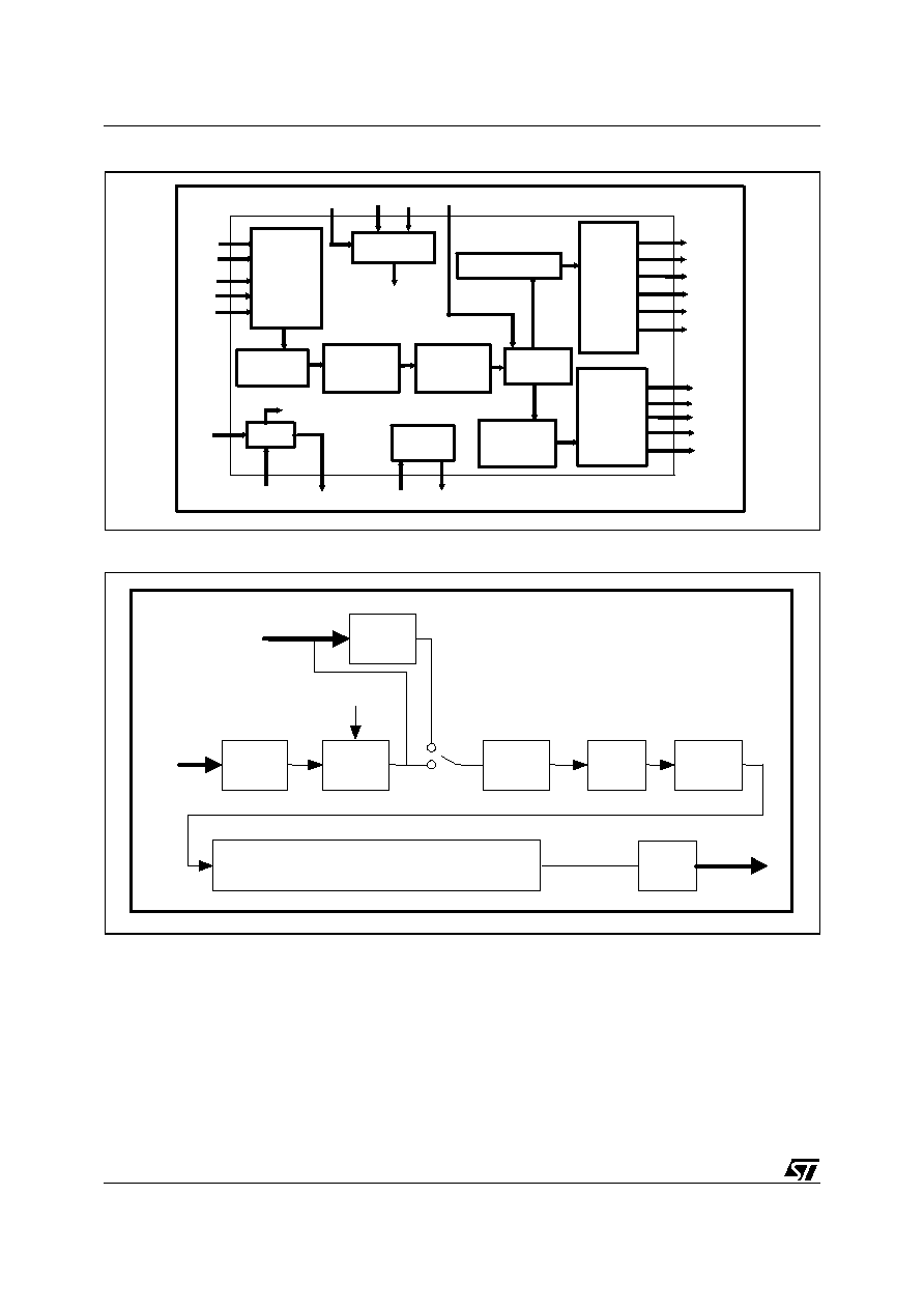
DESCRIPTION
The STA306 is a single chip solution for digital audio
processing and control in multi-channel applications.
It provides output capabilities for DDX
TM
(Direct Digi-
tal Amplification). In conjunction with a DDX
TM
power
device, it provides high-quality, high-efficiency, all
digital amplification. The device is extremely versatile
allowing for input of most digital formats including
192kHz, 24-bit DVD-Audio.
The internal 24-bit DSP allows for high resolution
processing at all standard input sample frequencies.
Processing includes volume control, filtering, bass
management, gain compression/limiting and PCM
and DDX
TM
outputs. Filtering includes five user-pro-
grammable 28-bit biquads for EQ per channel, as
well as bass, treble and DC blocking. External clock-
ing can be provided at 4 different ratios of the input
sample frequency. All sample frequencies are up-
sampled for processing. Each internal processing
channel can receive any input channel, allowing flex-
ibility and the ability to perform active digital cross-
over for powered loudspeaker systems.
The serial audio data interface accepts many differ-
ent formats, including the popular I2S format. STx-
channels of DDX processing are performed.
TQFP64
ORDERING NUMBER: STA306
PRODUCT PREVIEW
MULTICHANNEL DIGITAL AUDIO PROCESSOR WITH DDXTM
STA306
2/33
BLOCK DIAGRAM
Figure 1. Signal Flow Diagram
OUT1A/B
OUT2A/B
OUT3A/B
OUT4A/B
OUT5A/B
OUT6A/B
LRCKI
BICKI
SDI12
SDI34
SDI56
SA
SERIAL
DATA
IN
I
2
C
CHANNEL
MAPPING
VARIABLE
OVER-
SAMPLING
TREBLE,
BASS, EQ
(BIQUADS)
VOLUME
LIMITING
SDO12
SDO34
SDO56
OVERSAMPLING
VARIABLE
DOWN-
SAMPLING
POWER
DOWN
PWDN
EAPD
PLL
PLLB
XTI
CKOUT
SCL
SDA
LRCKO
BICKO
MVO
SERIAL
DATA
OUT
SYSTEM
CONTROL
SYSTEM TIMING
DDX
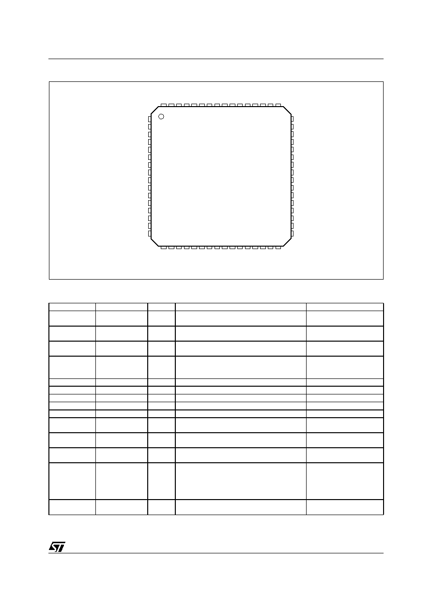
Channel
Mapping
1x,2x,4x
Interp
Biquads
B/T
Volume
Limiter
2x
Interp
Noise & Distortion Reduction
PWM
DDX
Output
Interp_Rate
6 Inputs
From I2S
Scale
& Mix
BME
Channels 1-6
1st Stage
Interpolation
Output
Bass Management
Channel
Mapping
1x,2x,4x
Interp
Biquads
B/T
Volume
Limiter
2x
Interp
Noise & Distortion Reduction
PWM
DDX
Output
Interp_Rate
6 Inputs
From I2S
Scale
& Mix
BME
Channels 1-6
1st Stage
Interpolation
Output
Bass Management
3/33
STA306
IN CONNECTION (Top view)
PIN FUNCTION
PIN
NAME
TYPE
DESCRIPTION
PAD TYPE
1
MVO
I
Master Volume Override
CMOS Input Buffer with
Pull-Down
3, 12, 24, 28,
35, 44, 52, 59
VDD3
3.3V Digital Supply
3.3V Digital Power
Supply Voltage (pad ring)
2, 4, 13, 27,
36, 45, 53, 60
GND
Digital Ground
Digital Ground
5, 14, 26, 37,
46, 54, 61
VDD
2.5V Digital Supply
2.5V Digital Power
Supply Voltage (core +
ring)
7
SDI_56
I
Input I2S Serial Data Channels 5 & 6
5V Tolerant TTL Input Buffer
8
SDI_34
I
Input I2S Serial Data Channels 3 & 4
5V Tolerant TTL Input Buffer
9
SDI_12
I
Input I2S Serial Data Channels 1 & 2
5V Tolerant TTL Input Buffer
10
LRCKI
I
Inputs I2C Left/Right Clock
5V Tolerant TTL Input Buffer
11
BICKI
I
Inputs I2C Serial Clock
5V Tolerant TTL Input Buffer
15
RESET
I
Global Reset
5V Tolerant TTL Schmitt
Trigger Input Buffer
16
PLLB
I
PLL Bypass
CMOS Input Buffer with
Pull-Down
17
SA
I
Select Address (I2C)
CMOS Input Buffer with
Pull-Down
18
SDA
I/O
I2C Serial Data
Bidirectional Buffer:
5V Tolerant TTL Schmitt
Trigger Input;
3.3V Capable 2 mA
Slew-rate control Output;
19
SCL
I
I2C Serial Clock
5V Tolerant TTL Schmitt
Trigger Input Buffer
1
2
3
5
6
4
7
8
9
10
27
11
28 29 30 31 32
59 58 57 56
54
55
53 52 51 50 49
43
42
41
39
38
40
48
47
46
44
45
N.C.
VDD
GND
TEST_MODE
MVO
VDD3
BICKI
LRCKI
SDI_12
SDI_56
SDI_34
VDDA
GNDA
VDD3
CKOUT
GND
VDD
VDD3
N.C.
N.C.
N.C.
N.C.
VDD3
SDO_34
SDO_12
LRCKO
VDD
BICKO
GND
VDD3
EAPD
OUT1_A
OUT1_B
OUT3_A
OUT3_B
OUT4_A
OUT5_A
OUT5_B
OUT4_B
OUT2_A
OUT2_B
VDD
VDD3
GND
D02AU1522
22 23 24 25 26
60
GND
61
VDD
62
SDO_56
63
N.C.
64
PWDN
SA
SDA
SCL
XTI
FILTER_PLL
17 18 19 20 21
37
36
34
33
35
VDD
GND
OUT6_A
OUT6_B
VDD3
12
13
14
15
16
PLLB
RESET
VDD
VDD3
GND

STA306
4/33
PIN
NAME
TYPE
DESCRIPTION
PAD TYPE
20
XTI
I
Crystal Oscillator Input (Clock Input)
3.3V Tolerant TTL Schmitt
Trigger Input Buffer
21
FILTER_PLL
PLL Filter
Analog Pad
22
VDDA
PLL 2.5V Supply
2.5V Analog Power
Supply Voltage
23
GNDA
PLL Ground
Analog Ground
25
CKOUT
O
Clock Output
3.3V Capable TTL Tristate
4mA Output Buffer
33
OUT6_B
O
PWM Channel 6 Output B
3.3V Capable TTL 2mA
Output Buffer
34
OUT6_A
O
PWM Channel 6 Output A
3.3V Capable TTL 2mA
Output Buffer
38
OUT5_B
O
PWM Channel 5 Output B
3.3V Capable TTL 2mA
Output Buffer
39
OUT5_A
O
PWM Channel 5 Output A
3.3V Capable TTL 2mA
Output Buffer
40
OUT4_B
O
PWM Channel 4 Output B
3.3V Capable TTL 2mA
Output Buffer
41
OUT4_A
O
PWM Channel 4 Output A
3.3V Capable TTL 2mA
Output Buffer
42
OUT3_B
O
PWM Channel 3 Output B
3.3V Capable TTL 2mA
Output Buffer
43
OUT3_A
O
PWM Channel 3 Output A
3.3V Capable TTL 2mA
Output Buffer
47
OUT2_B
O
PWM Channel 2 Output B
3.3V Capable TTL 2mA
Output Buffer
48
OUT2_A
O
PWM Channel 2 Output A
3.3V Capable TTL 2mA
Output Buffer
49
OUT1_B
O
PWM Channel 1 Output B
3.3V Capable TTL 2mA
Output Buffer
50
OUT1_A
O
PWM Channel 1 Output A
3.3V Capable TTL 2mA
Output Buffer
51
EAPD
O
External Amplifier Power Down
3.3V Capable TTL 2mA
Output Buffer
55
BICKO
O
Output I2S Serial Clock
3.3V Capable TTL 2mA
Output Buffer
56
LRCKO
O
Output I2S Left/Right Clock
3.3V Capable TTL 2mA
Output Buffer
57
SDO_12
O
Output I2S Serial Data Channels 1 & 2
3.3V Capable TTL 2mA
Output Buffer
58
SDO_34
O
Output I2S Serial Data Channels 3 & 4
3.3V Capable TTL 2mA
Output Buffer
62
SDO_56
O
Output I2S Serial Data Channels 5 & 6
3.3V Capable TTL 2mA
Output Buffer
63
SDO_78
O
Output I2S Serial Data Channels 7 & 8
3.3V Capable TTL 2mA
Output Buffer
64
PWDN
I
Device Powerdown
5V Tolerant TTL Schmitt
Trigger Input Buffer
PIN FUNCTION (continued)
5/33
STA306
ABSOLUTE MAXIMUM RATINGS
THERMAL DATA
RECOMMENDED DC OPERATING CONDITIONS
Symbol
Parameter
Value
Unit
V
DD_3.3
3.3V I/O Power Supply
-0.5 to 4
V
V
DD_2.5
2.5V Logic Power Supply
-0.5 to 3.3
V
V
i
Voltage on input pins
-0.5 to (VDD+0.5)
V
V
o
Voltage on output pins
-0.5 to (VDD+0.3)
V
T
stg
Storage Temperature
-40 to +150
∞
C
T
amb
Ambient Operating Temperature
-20 to +85
∞
C
Symbol
Parameter
Value
Unit
R
thj-amb
Thermal resistance Junction to Ambient
85
∞
C/W
Symbol
Parameter
Value
Unit
V
DD_3.3
I/O Power Supply
3.0 to 3.6
V
V
DD_2.5
Logic Power Supply
2.3 to 2.7
V
T
j
Operating Junction Temperature
-20 to +125
∞
C