
ST75C520
HIGH SPEED FAX MODEM DATA PUMP
June 1995
PRELIMINARY DATA
PQFP64
(Plastic Quad Flat Pack)
ORDER CODE : ST75C520 PQFP
.
ITU-T V.17, V.29, V.27ter, V.21 WITH FAX
SUPPORT
.
ITU-T V.23, V.21, BELL 103
.
V.17, V.29 (T104), V.27ter SHORT TRAINS
.
V.33 HALF-DUPLEX
.
1800Hz OR 1700Hz CARRIER
.
SINGLE CHIP COMPLETE DATA PUMP
.
SINGLE 5V POWER SUPPLY :
- TYPICAL ACTIVE POWER CONSUMPTION :
375mW
- LOW POWER MODE (typ. 5mW)
.
EXTENDED MODES OF OPERATIONS :
- FULL IMPLEMENTATION OF THE V.17,
V.33, V.29 AND V.27ter HANDSHAKES
- AUTODIAL AND AUTOANSWER CAPABIL-
ITY
- PROGRAMMABLE TONE DETECTION AND
FSK V.21 FLAG PATTERN DETECTION
DURING HIGH SPEED RECEPTION
- PROGRAMMABLE CALL PROGRESS AND
CALL WAITING TONE DETECTORS IN-
CLUDING DTMF
- PROGRAMMABLE CLASS
TM
DETECTION
CAPABILITY
- WIDE DYNAMIC RANGE (>48dB)
- A-LAW VOICE PCM MODE
.
VERSATILE INTERFACES :
- PARALLEL 64 x 8-BIT DUAL PORT RAM
- SYNCHRONOUS/HDLC PARALLEL DATA
HANDLING
- HDLC FRAMING SUPPORT
- V.24 INTERFACE
- FULL OPERATING STATUS REAL TIME
MONITORING
- FULL DIAGNOSTIC CAPABILITY
- DUAL 8-BIT DAC FOR CONSTELLATION
DISPLAY
DESCRIPTION
The SGS-THOMSON Microelectronics ST75C520
chip is a highly integrated modem engine, which
can operate with all currently used FAX group III
standards up to 14400bps. Full V.21, V.23 and Bell
103 full duplex
modem standards are imple-
mented.
This is advance information on a new product now in development or undergoing evaluation. Details are subject to change without no tice.
1/45

CONTENTS
Page
I
PIN DESCRIPTION . . . . . . . . . . . . . . . . . . . . . . . . . . . . . . . . . . . . . . . . . . . . . . . . . . . .
3
I.1
PIN CONNECTIONS. . . . . . . . . . . . . . . . . . . . . . . . . . . . . . . . . . . . . . . . . . . . . . . . . . . .
3
I.2
HOST INTERFACE. . . . . . . . . . . . . . . . . . . . . . . . . . . . . . . . . . . . . . . . . . . . . . . . . . . . .
3
I.3
ANALOG INTERFACE . . . . . . . . . . . . . . . . . . . . . . . . . . . . . . . . . . . . . . . . . . . . . . . . . .
4
I.4
V.24 INTERFACE . . . . . . . . . . . . . . . . . . . . . . . . . . . . . . . . . . . . . . . . . . . . . . . . . . . . . .
4
I.5
MISCELLANOUS . . . . . . . . . . . . . . . . . . . . . . . . . . . . . . . . . . . . . . . . . . . . . . . . . . . . . .
4
I.6
BOUNDARY SCAN INTERFACE . . . . . . . . . . . . . . . . . . . . . . . . . . . . . . . . . . . . . . . . . .
4
I.7
POWER SUPPLY . . . . . . . . . . . . . . . . . . . . . . . . . . . . . . . . . . . . . . . . . . . . . . . . . . . . . .
5
II
BLOCK DIAGRAMS. . . . . . . . . . . . . . . . . . . . . . . . . . . . . . . . . . . . . . . . . . . . . . . . . . . .
5
III
ELECTRICAL SPECIFICATIONS . . . . . . . . . . . . . . . . . . . . . . . . . . . . . . . . . . . . . . . . .
6
III.1
MAXIMUM RATINGS . . . . . . . . . . . . . . . . . . . . . . . . . . . . . . . . . . . . . . . . . . . . . . . . . . .
6
III.2
DC CHARACTERISTICS . . . . . . . . . . . . . . . . . . . . . . . . . . . . . . . . . . . . . . . . . . . . . . . .
6
III.3
AC CHARACTERISTICS . . . . . . . . . . . . . . . . . . . . . . . . . . . . . . . . . . . . . . . . . . . . . . . .
8
IV
FUNCTIONAL DESCRIPTION . . . . . . . . . . . . . . . . . . . . . . . . . . . . . . . . . . . . . . . . . . . .
10
IV.1
SYSTEM ARCHITECTURE . . . . . . . . . . . . . . . . . . . . . . . . . . . . . . . . . . . . . . . . . . . . . .
10
IV.2
OPERATION. . . . . . . . . . . . . . . . . . . . . . . . . . . . . . . . . . . . . . . . . . . . . . . . . . . . . . . . . .
10
IV.3
MODEM INTERFACE . . . . . . . . . . . . . . . . . . . . . . . . . . . . . . . . . . . . . . . . . . . . . . . . . . .
11
V.
USER INTERFACE. . . . . . . . . . . . . . . . . . . . . . . . . . . . . . . . . . . . . . . . . . . . . . . . . . . . .
11
V.1
DUAL PORT RAM DESCRIPTION . . . . . . . . . . . . . . . . . . . . . . . . . . . . . . . . . . . . . . . . .
11
V.2
COMMAND SET . . . . . . . . . . . . . . . . . . . . . . . . . . . . . . . . . . . . . . . . . . . . . . . . . . . . . . .
14
V.3
COMMAND SET SHORT FORM . . . . . . . . . . . . . . . . . . . . . . . . . . . . . . . . . . . . . . . . . .
16
V.4
STATUS - REPORTS . . . . . . . . . . . . . . . . . . . . . . . . . . . . . . . . . . . . . . . . . . . . . . . . . . .
17
V.5
DATA EXCHANGES. . . . . . . . . . . . . . . . . . . . . . . . . . . . . . . . . . . . . . . . . . . . . . . . . . . .
17
VI
COMMAND SET DESCRIPTION . . . . . . . . . . . . . . . . . . . . . . . . . . . . . . . . . . . . . . . . . .
18
VII
STATUS DESCRIPTION . . . . . . . . . . . . . . . . . . . . . . . . . . . . . . . . . . . . . . . . . . . . . . . .
27
VII.1
COMMAND ACKNOWLEDGE AND REPORT . . . . . . . . . . . . . . . . . . . . . . . . . . . . . . . .
27
VII.2
MODEM STATUS . . . . . . . . . . . . . . . . . . . . . . . . . . . . . . . . . . . . . . . . . . . . . . . . . . . . . .
28
VIII
TONE DETECTORS . . . . . . . . . . . . . . . . . . . . . . . . . . . . . . . . . . . . . . . . . . . . . . . . . . . .
34
VIII.1
OVERVIEW. . . . . . . . . . . . . . . . . . . . . . . . . . . . . . . . . . . . . . . . . . . . . . . . . . . . . . . . . . .
34
VIII.2
DESCRIPTION . . . . . . . . . . . . . . . . . . . . . . . . . . . . . . . . . . . . . . . . . . . . . . . . . . . . . . . .
34
VIII.3
EXAMPLE . . . . . . . . . . . . . . . . . . . . . . . . . . . . . . . . . . . . . . . . . . . . . . . . . . . . . . . . . . . .
38
IX
BUFFER OPERATIONS. . . . . . . . . . . . . . . . . . . . . . . . . . . . . . . . . . . . . . . . . . . . . . . . .
38
IX.1
INTRODUCTION. . . . . . . . . . . . . . . . . . . . . . . . . . . . . . . . . . . . . . . . . . . . . . . . . . . . . . .
38
IX.2
RECEIVE OPERATIONS OVERVIEW . . . . . . . . . . . . . . . . . . . . . . . . . . . . . . . . . . . . . .
39
IX.3
TRANSMIT OPERATIONS OVERVIEW. . . . . . . . . . . . . . . . . . . . . . . . . . . . . . . . . . . . .
39
IX.4
BUFFER STATUS AND FORMAT DESCRIPTION . . . . . . . . . . . . . . . . . . . . . . . . . . . .
40
IX.5
RECEIVE BUFFER . . . . . . . . . . . . . . . . . . . . . . . . . . . . . . . . . . . . . . . . . . . . . . . . . . . . .
40
IX.6
DATA BUFFER MANAGEMENT. . . . . . . . . . . . . . . . . . . . . . . . . . . . . . . . . . . . . . . . . . .
40
X
DEFAULT CALL PROGRESS TONE DETECTORS . . . . . . . . . . . . . . . . . . . . . . . . . . .
42
XI
DEFAULT ANSWER TONE DETECTORS . . . . . . . . . . . . . . . . . . . . . . . . . . . . . . . . . .
42
XII
ELECTRICAL SCHEMATICS. . . . . . . . . . . . . . . . . . . . . . . . . . . . . . . . . . . . . . . . . . . . .
42
XIII
PCB DESIGN GUIDELINES. . . . . . . . . . . . . . . . . . . . . . . . . . . . . . . . . . . . . . . . . . . . . .
43
ST75C520
2/45

1
2
3
4
5
6
7
8
9
10
11
12
13
14
15
16
17
18
19
20
21
22
23
24
25
26
27
28
29
30
31
32
64
63
62
61
60
59
58
57
56
55
54
53
52
51
50
49
38 39 40 41 42 43 44 45 46 47 48
33 34 35 36 37
AGNDT
RXA2
RXA1
AGNDR
EXTAL
XTAL
CLKOUT
HALT
RESET
SCOUT
BOS
EOS
SA0
SA1
SA2
SA3
SA4
SA5
SA6
GND
SD0
SD1
SD2
SD3
SD4
SD5
SD6
TXD
RXD
CLK
CD
CTS
GND
EYEX
EYEY
TEST2
EBS
TXA2
TXA1
RTS
RING
SD7
SDS
(SRD)
SR/W
(SWR)
SCS
SDTACK
SINTR
INT/MOT
GND
SCIN
SCCLK
MCI
RDYS
MC2
MC1
MC0
V
DD
TEST1
DD
V
V
CM
V
REFP
V
REFN
AV
DD
V
DD
75C52001.EPS
I - PIN DESCRIPTION
I.1 - Pin Connections
I.2 - Host Interface
The exchanges with the control processor proceed through a 64 Bytes DUAL port RAM shared between
the ST75C520 and the Host. The signals associated with this interface are :
Pin Name
Type
Description
SD0..SD7
I/O
System Data Bus. 8-bit data bus used for asynchronous exchanges between the ST75C520
and the Host through the dual port RAM. High impedance when exchanges are not active.
SA0..SA6
I
System Address Bus. 7-bit address bus for dual port RAM.
SDS (SRD)
I
System Data Strobe. Active low. Synchronizes all the exchanges. In Motorola mode initiates
the exchange, active low. In Intel mode initiates a read exchange, active low.
SR/W (SWR)
I
System Read/Write. In Motorola mode defines the type of exchange read/write. In Intel
mode initiates a write exchange, active low.
SCS
I
System Chip Select. Active low.
SDTACK
OD
System Bus Data Acknowledge. Active low. Open drain.
SINTR
OD
System Interrupt Request. Active low. This signal is asserted by the ST75C520 and
negated by the host. Open drain.
RESET
I
Reset. Active low.
RING
I
Ring Detect Signal. Active low.
INT/MOT
I
Select Intel/Motorola Interface.
ST75C520
3/45

I.3 - Analog Interface
Pin
Name
Type
Description
TXA1
O
Transmit Analog Output 1
TXA2
O
Transmit Analog Output 2. Outputs TXA1 and TXA2 provide analog signals with maximum peak to peak
amplitude 2 x V
REF
, and must be followed by an external continous-time two pole smoothing filter (where
V
REF
= V
REFP
- V
REFN
).
RXA1
I
Receive Analog Input 1
RXA2
I
Receive Analog Input 2. The analog differential input peak to peak signal must be less than 2 x V
REF
. It
must be preceded by an external continous-time single pole anti-aliasing filter. This filter must be as
close as possible to the RXA1 and RXA2 Pins (where V
REF
= V
REFP
- V
REFN
).
V
CM
I/O
Analog Common Voltage (nominal +2.5V). This input must be decoupled with respect to AGND.
V
REFN
I
Analog Negative Reference (nominal V
CM
- 1.25V). This input must be decoupled with respect to V
CM
.
V
REFP
I
Analog Positive Reference (nominal V
CM
+1.25V). This input must be decoupled with respect to V
CM
.
I.4 - V.24 Interface
Pin Name
Type
Description
RTS
I
Request to Send. Active low.
CLK
O
Data Bit Clock. Falling edge co�ncides with DATA change.
CTS
O
Clear to Send. Active low.
RxD
O
Receive Data
TxD
I
Transmit Data sampled with rising edge of CLK
CD
O
Carrier Detect. Active low.
I.5 - Miscellaneous
Pin Name
Type
Description
XTAL
O
Internal Oscillator Output. Left open if not used.
EXTAL
I
Internal Oscillator Input, or External Clock
EYEX
O
Constellation X analog coordinate
EYEY
O
Constellation Y analog coordinate
TEST1
To be left open
TEST2
To be left open
Note : The nominal external clock frequency of the ST75C520 is 29.4912MHz with a precision better than
�
5.10
-5
I.6 - Boundary Scan Interface
A set of 13 signals are dedicated for Testing the ST75C520 Component. These signals can be used in a
development phase, associated with the SGS-THOMSON ST18932 Boundary Scan Development Tools,
to Debug the application Hardware and Software. If not used all input signals must be grounded and all
output signals left open.
Pin Name
Type
Description
SCIN
I
Scan Data Input
SCCLK
I
Scan Clock
SCOUT
O
Scan Data Output
BOS
I
Begin of Scan Control
EOS
I
End of Scan
MC0..MC2
I
Mode Control
HALT
I
Stop ST75C520 Execution
MCI
O
Multicycle Instruction
RDYS
O
Ready to Scan Flag
EBS
I
Enable Boundary Scan. Active low (must be set low in normal mode).
CLKOUT
O
Internal ST75C520 Clock (XTAL frequency divided by 2)
ST75C520
4/45
I.7 - Power Supply
Symbol
Parameter
V
DD
Digital +5V (Pin 9, 25, 41). To be connected to AV
DD
(see below).
GND
Digital Ground (Pin 8, 24, 40). To be connected to AGNDT and AGNDR (see below).
AV
DD
Analog +5V (Pin 62). To be connected to V
DD
(see below).
AGNDT
Analog Transmit Ground (Pin 64). To be connected to GND (see below).
AGNDR
Analog Receive Ground (Pin 59). To be connected to GND (see below).
AGNDT and AGNDR must be connected together as close as possible to the chip.
GND and AGNDR board plans should be separated, then connected together as close as possible to the
chip, at a single point. Similarly V
DD
and AV
DD
must ne connected as close as possible to the chip, at a
single point.
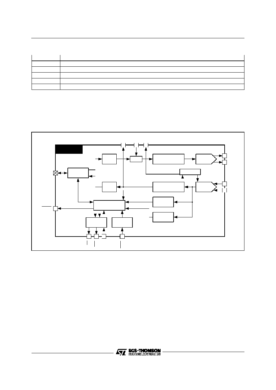
V.21 FLAG
DETECTOR
TONE
DETECTOR
RING
DETECTOR
V.24
INTERFACE
HANDSHAKE AND
STATUS REPORT
V.17, V.29, V.27
FAX RECEIVER
RX
ANALOG
TX
ANALOG
V.17, V.29, V.27
FAX TRANSMITTER
HDLC
RX
DUAL RAM
INTERFACE
HDLC
TX
MUX
DPLL
38
13
11
12
10
15
16
14
1
2
60
61
TXA1
TXA2
RXA1
RXA2
SD [0..7]
(26 to 33)
SINTR
RXD
TXD
CLK
CD
CTS
RTS
RING
ST75C520
75C52002.EPS
II - BLOCK DIAGRAMS
II.1 - Functional Block Diagram
ST75C520
5/45