July 2006
Rev 1
1/22
22
PD57070-E
PD57070S-E
RF POWER Transistors, LDMOST plastic family
N-Channel enhancement-mode lateral MOSFETs
General features
Excellent thermal stability
Common source configuration
P
OUT
= 70W with 14.7dB gain @ 945MHz / 28V
New RF plastic package
Description
The PD57070 is a common source N-Channel,
enhancement-mode lateral Field-Effect RF power
transistor. It is designed for high gain, broad band
commercial and industrial applications. It
operates at 28 V in common source mode at
frequencies of up to 1 GHz. PD57070 boasts the
excellent gain, linearity and reliability of ST's
latest LDMOS technology mounted in the first
true SMD plastic RF power package, PowerSO-
10RF. PD57070's superior linearity performance
makes it an ideal solution for base station
applications.
The PowerSO-10 plastic package, designed to
offer high reliability, is the first ST JEDEC
approved, high power SMD package. It has been
specially optimized for RF needs and offers
excellent RF performances and ease of
assembly.
Mounting recommendations are available in
www.st.com/rf/ (look for application note AN1294)
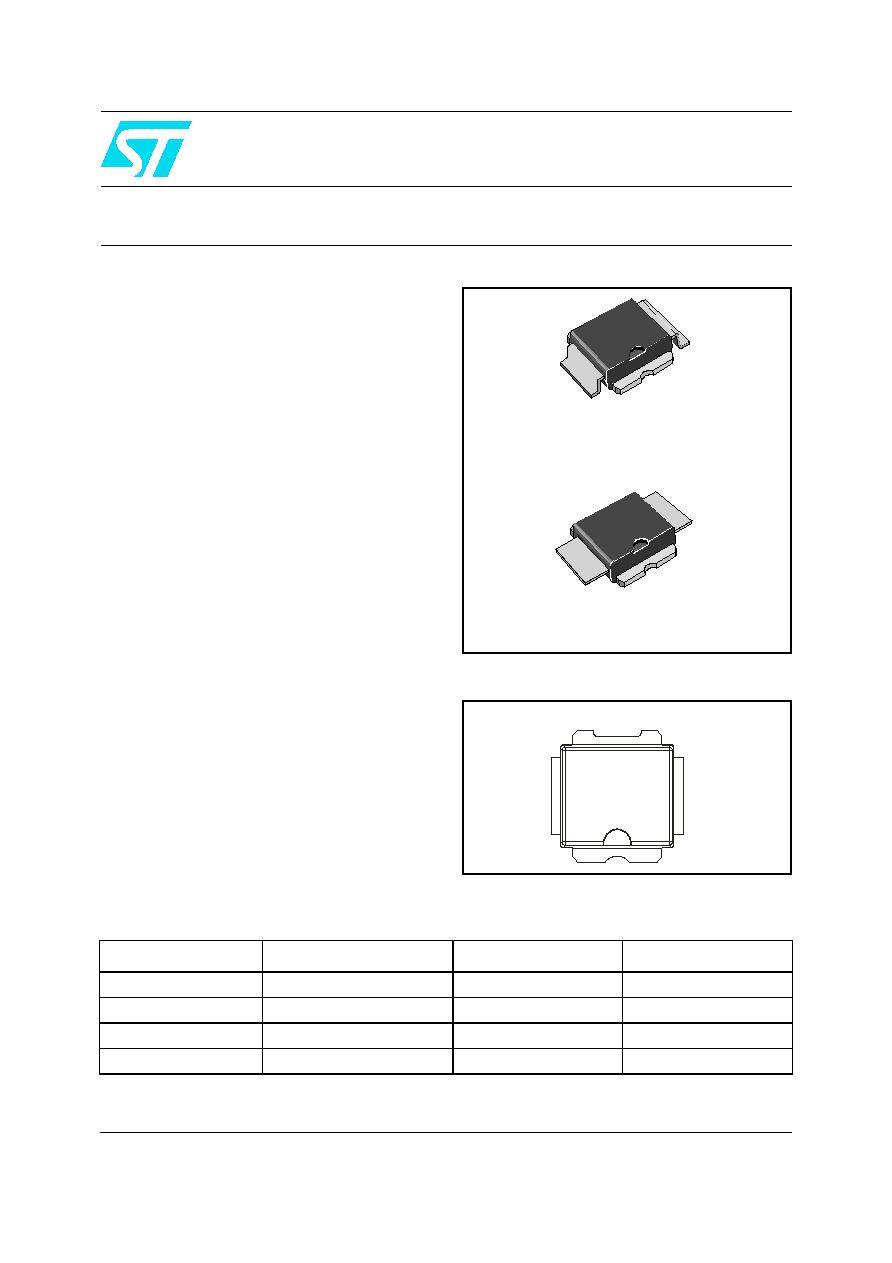
Pin connection
PowerSO-10RF
(formed lead)
PowerSO-10RF
(straight lead)
Gate
Source
Drain
www.st.com
Order codes
Part number
Package
Marking
Packaging
PD57070-E
PowerSO-10RF (formed lead)
PD57070
Tube
PD57070S-E
PowerSO-10RF (straight lead)
PD57070S
Tube
PD57070TR-E
PowerSO-10RF (formed lead)
PD57070
Tape and reel
PD57070STR-E
PowerSO-10RF (straight lead)
PD57070S
Tape and reel

Contents
PD57070-E, PD57070S-E
2/22
Contents
1
Electrical data . . . . . . . . . . . . . . . . . . . . . . . . . . . . . . . . . . . . . . . . . . . . . . 3
1.1
Maximum ratings . . . . . . . . . . . . . . . . . . . . . . . . . . . . . . . . . . . . . . . . . . . . 3
1.2
Thermal data . . . . . . . . . . . . . . . . . . . . . . . . . . . . . . . . . . . . . . . . . . . . . . . 3
2
Electrical characteristics . . . . . . . . . . . . . . . . . . . . . . . . . . . . . . . . . . . . . 4
2.1
Static . . . . . . . . . . . . . . . . . . . . . . . . . . . . . . . . . . . . . . . . . . . . . . . . . . . . . 4
2.2
Dynamic . . . . . . . . . . . . . . . . . . . . . . . . . . . . . . . . . . . . . . . . . . . . . . . . . . . 4
3
Impedances . . . . . . . . . . . . . . . . . . . . . . . . . . . . . . . . . . . . . . . . . . . . . . . . 5
4
Typical performance (PD57070S) . . . . . . . . . . . . . . . . . . . . . . . . . . . . . . . 6
5
Test circuit . . . . . . . . . . . . . . . . . . . . . . . . . . . . . . . . . . . . . . . . . . . . . . . . . 9
6
Common source s-parameter . . . . . . . . . . . . . . . . . . . . . . . . . . . . . . . . 12
6.1
PD57070S(VDS = 28V IDS = 500mA) . . . . . . . . . . . . . . . . . . . . . . . . . . . 12
6.2
PD57070S (VDS = 28V IDS = 1A) . . . . . . . . . . . . . . . . . . . . . . . . . . . . . . 13
6.3
PD57070S (VDS = 28V IDS = 2A) . . . . . . . . . . . . . . . . . . . . . . . . . . . . . . 14
6.4
PD57070S (VDS = 28V IDS = 3A) . . . . . . . . . . . . . . . . . . . . . . . . . . . . . . 15
7
Package mechanical data . . . . . . . . . . . . . . . . . . . . . . . . . . . . . . . . . . . . 16
8
Revision history . . . . . . . . . . . . . . . . . . . . . . . . . . . . . . . . . . . . . . . . . . . 21
PD57070-E, PD57070S-E
Electrical data
3/22
1 Electrical
data
1.1 Maximum
ratings
1.2 Thermal
data
Table 1.
Absolute maximum ratings (T
CASE
= 25�C)
Symbol
Parameter
Value
Unit
V
(BR)DSS
Drain-Source Voltage
65
V
V
GS
Gate-Source Voltage
� 20
V
I
D
Drain Current
7
A
P
DISS
Power Dissipation (@ Tc = 70�C)
95
W
T
J
Max. Operating Junction Temperature
165
�C
T
STG
Storage Temperature
-65 to +150
�C
Table 2.
Thermal data
Symbol
Parameter
Value
Unit
R
thJC
Junction - case thermal resistance
1.0
�C/W