 | –≠–Ľ–Ķ–ļ—ā—Ä–ĺ–Ĺ–Ĺ—č–Ļ –ļ–ĺ–ľ–Ņ–ĺ–Ĺ–Ķ–Ĺ—ā: CXD4017R | –°–ļ–į—á–į—ā—Ć:  PDF PDF  ZIP ZIP |

≠ 1 ≠
CXD4017R
64 pin LQFP (Plastic)
Reception Digital Signal Processor IC for Infrared Spatial Digital Audio Communication
Description
The CXD4017R is an IC that processes the
received digital signals used for infrared spatial digital
audio communication (based on the IEC61603-8-1
standard) in consumer products. This IC contains the
analog-to-digital converter (ADC) for RF signal
applications and a PLL circuit for audio applications.
Features
∑ Performs all the received digital signal processing
on a single chip.
∑ Supports the infrared spatial digital audio
communication system formats for consumer
uses.
∑ Direct input of RF signals enabled by on-chip
ADC.
∑ External RAM and PLL circuit not required.
Demodulator Block
∑ Digital processing throughout enables the received
RF signals in the infrared spatial digital audio
communication system formats to be processed
directly.
∑ External analog circuit can be simplified by digital
filter and on-chip ADC for RF signal applications.
∑ Reproduction of subcarrier processed digitally.
Error Corrector Block
∑ Enables error correction for infrared spatial digital
audio communication system formats.
Output Interface Block
∑ Digital-to-analog converter (DAC) for various audio
applications can be connected directly.
Controller Block
∑ Simple pin setting mode
∑ Serial interface provided by serial bus
∑ Enables output of error correction state.
PLL Block
∑ On-chip PLL circuit for reproducing the clock
signals required by the infrared spatial digital
audio communication system formats.
Structure
Silicon gate CMOS IC
Absolute Maximum Ratings
∑ Supply voltage
V
DD1
≠0.5 to +3.0
V
V
DDE
≠0.5 to +3.0
V
∑ Input voltage
V
I
≠0.5 to V
DDE
+ 0.5 V
(
3.0V)
∑ Output voltage
V
O
≠0.5 to V
DDE
+ 0.5 V
(
3.0V)
∑ Storage temperature
Tstg
≠55 to +125
įC
Recommended Operating Conditions
∑ Supply voltage
V
DDI
1.5 Ī 0.1
V
V
DDE
2.5 Ī 0.2
V
∑ A/D supply voltage
V
AD
2.5 Ī 0.2
V
∑ PLL supply voltage
V
PLL
1.5 Ī 0.1
V
∑ Operating temperature
Topr
≠40 to +85
įC
Input/Output Capacitance
∑ Input capacitance
C
IN
16 (max.)
pF
∑ Output capacitance
C
OUT
16 (max.)
pF
Note: Measurement conditions:
Tj = 25įC, V
DD
= V
I
= 0V, f = 1MHz
∑ Analog input capacitance
C
AD
12 (typ.)
pF
E03970B49-PS
Sony reserves the right to change products and specifications without prior notice. This information does not convey any license by
any implication or otherwise under any patents or other right. Application circuits shown, if any, are typical examples illustrating the
operation of the devices. Sony cannot assume responsibility for any problems arising out of the use of these circuits.

≠ 2 ≠
CXD4017R
Block Diagram
Test pins not shown.
APCPO
APVCI
PLVAR
PLREF
V
SS
V
SS
V
SS
V
SS
V
SS
V
SS
V
DDE
V
DDE
V
DDE
V
DDE
V
DDE
V
DDI
V
DDI
V
SS
38
58
26
56
41
27
11
4
57
42
39
25
21
12
5
37
36
35
34
33
63
61
60
59
54
31
24
23
22
20
18
62
30
29
15
14
13
28
32
ADVRH
ADAVS
ADAVD
ADVRL
ADVIN
XRST
DIFM0
DIFM1
CHNUM
DIVCODE
CSOD
SRDT
SWDT
XSCEN
SCLK
SCMODE
EXTCK
BCK
LRCK
DAOUT
DTVALID
EMPFS0
EMPFS1
APAVD
APAVS
APX
VCOR
OSCI
OSCO
A/D
Converter
Demodulator
Error
Corrector
Output
I/F
Clock
Selector
Buffer
RAM
Clock
Generator
Controller
PLL
17
40
43
6
7
8
9
10

≠ 3 ≠
CXD4017R
Pin Configuration
TEST12
TEST14
TEST13
V
DDE
V
SS
ADAVS
ADVRH
ADAVD
ADVRL
V
DDE
ADVIN
V
SS
XRST
DIFM1
DIFM0
TEST15
TEST4
TEST2
TEST3
TEST1
TEST0
V
SS
OSCO
V
DDE
OSCI
SCMODE
V
SS
SCLK
XSCEN
SRDT
SWDT
CSOD
EXTCK
DIVCODE
VCOR
V
DDI
APX
CHNUM
V
DDE
APAVS
V
SS
APCPO
APVCI
PLVAR
APAVD
V
SS
TEST16
PLREF
TEST5
TEST7
TEST9
TEST10
TEST6
TEST8
BCK
V
SS
V
DDE
LRCK
DTVALID
EMPFS1
V
DDI
DAOUT
EMPFS0
TEST11
1
2
3
4
5
6
9
10
11
12
13
14
15
16
17
18
19
20
21
22
23
24
25
26
27
28
29
30
31
32
64
63
62
61
60
59
58
57
56
55
54
53
52
51
50
49
48
47
46
45
44
43
42
41
40
39
38
37
36
35
34
33
7
8

≠ 4 ≠
CXD4017R
Pin Description
Pin
No.
Symbol
I/O
Description
1
2
3
4
5
6
7
8
9
10
11
12
13
14
15
16
17
18
19
20
21
22
23
24
25
26
27
28
29
30
31
32
33
34
35
36
37
TEST12
TEST13
TEST14
V
DDE
V
SS
ADVRH
ADAVS
ADAVD
ADVRL
ADVIN
V
DDE
V
SS
XRST
DIFM0
DIFM1
TEST15
PLREF
PLVAR
TEST16
APVCI
V
SS
APCPO
APAVD
APAVS
V
SS
V
DDI
V
DDE
VCOR
CHNUM
DIVCODE
APX
EXTCK
CSOD
SRDT
SWDT
XSCEN
SCLK
I
I
I
--
--
I
--
--
I
I
--
--
I
I
I
I
O
O
I
I
--
O
--
--
--
--
--
I
I
I
O
I
O
O
I
I
I
Test pin, normally fixed at low
Test pin, normally fixed at high
Test pin, normally fixed at high
Digital I/O power supply
Digital GND
RF ADC reference voltage input (high)
RF ADC analog GND
RF ADC analog power supply
RF ADC reference voltage input (low)
RF ADC input
Digital I/O power supply
Digital GND
Reset (negative logic)
Audio output format selection
Test pin, normally fixed at low
PLL reference output (fs)
PLL frequency-divided output (APX output or VCOR input divided by 256)
Test pin, normally fixed at low
PLL VCO control voltage input
Digital GND
PLL charge pump output
PLL VCO power supply
PLL VCO GND
Digital GND
Digital internal power supply
Digital I/O power supply
Data output clock input
Channel number selection (low: Ch0, high: Ch1)
Full/half-band mode selection (low: full-band, high: half-band)
PLL VCO output
Data output clock selection (low: APX internal connection, high: VCOR pin input)
Chapter start delay output
Serial interface data read output
Serial interface data write output
Serial interface data enable input (negative logic)
Serial interface data clock input

≠ 5 ≠
CXD4017R
Pin
No.
Symbol
I/O
Description
38
39
40
41
42
43
44
45
46
47
48
49
50
51
52
53
54
55
56
57
58
59
60
61
62
63
64
SCMODE
V
SS
OSCI
V
DDE
V
SS
OSCO
TEST0
TEST1
TEST2
TEST3
TEST4
TEST5
TEST6
TEST7
TEST8
TEST9
BCK
TEST10
V
DDE
V
SS
V
DDI
LRCK
DAOUT
DTVALID
EMPFS0
EMPFS1
TEST11
I
--
I
--
--
O
I
I
I
I
I
I
I
I
O
O
O
O
--
--
--
O
O
O
O
O
I
Control mode selection (low: pin setting, high: serial setting)
Digital GND
Crystal oscillator circuit input (12.288MHz)
Digital I/O power supply
Digital GND
Crystal oscillator circuit output (12.288MHz)
Test pin, normally fixed at low
Test pin, normally fixed at low
Test pin, normally fixed at low
Test pin, normally fixed at low
Test pin, normally fixed at low
Test pin, normally fixed at low
Test pin, normally fixed at low
Test pin, normally fixed at low
Test pin, normally open
Test pin, normally open
Bit clock output
Test pin, normally open
Digital I/O power supply
Digital GND
Digital internal power supply
Audio sample clock output
Output data for audio DAC
Data valid flag output (DTVALID, low: invalid, high: valid)
Emphasis, fs information output
Test pin, normally fixed at high

≠ 6 ≠
CXD4017R
Electrical Characteristics
1. DC characteristics
(V
DDE
= 2.5 Ī 0.2V, V
DDI
= 1.5 Ī 0.1V, V
SS
= 0V, Topr = ≠40 to +85įC)
Item
High level input voltage
Low level input voltage
High level output voltage
Low level output voltage
High level output current
Low level output current
Input leakage current
Crystal
connection pin
PLL supply voltage
PLL charge pump
output voltage
PLL VCO control voltage
ADC supply voltage
ADC reference voltage
(high)
ADC reference voltage
(low)
ADC reference potential
difference (1)
ADC reference input
resistance (2)
ADC input voltage
ADC input capacitance
ADC offset
Digital block supply current
internal logic
Digital block supply current
I/O
ADC block supply current
PLL block supply current
Reference voltage pin
current of A/D block
V
IH
V
IL
V
OH
V
OL
I
OH
I
OL
I
L
V
IH
V
IL
V
PLL
V
CPO
V
VCI
V
AD
V
RH
V
RL
V
RW
R
RW
V
IA
C
AD
V
OFF
I
DDI
I
DDE
I
AD
I
PLL
I
REF
Symbol
I
OH
= ≠100ĶA
I
OL
= 100ĶA
V
OH
= V
DDE
≠ 0.4V
V
OL
= 0.4V
V
DDI
= 1.5V
V
DDE
= 2.5V
V
AD
= 2.5V
V
PLL
= 1.5V
V
RW
= 2.0V
Conditions
1.7
≠0.3
V
DD
≠ 0.2
0
≠4.0
≠8.0
4.0
8.0
--
1.7
≠0.3
1.4
0
0
2.3
1.0
0.0
1.0
140
V
RL
Min.
--
--
--
--
--
--
--
--
--
1.5
2.5
2.0
--
2.0
280
--
12
20
7.5
3.2
6.7
0.5
7.2
Typ.
V
DDE
+ 0.3
0.7
V
DDE
0.2
--
--
--
--
Ī5
V
DDE
+ 0.3
0.7
1.6
V
PLL
V
PLL
2.7
V
AD
V
AD
≠ 1.0
2.1
V
RH
14.3
Max.
V
mA
ĶA
V
V
V
V
V
V
V
V
V
V
pF
mV
mA
Unit
1
2, 3, 4
2, 3
4
2, 3
4
1
5
5
6
7
8
9
10
11
12
13
9
6
10
Applicable pins
Note 1: V
RW
= V
RH
≠ V
RL
Note 2: A current of approximately 7.2mA (typ.), 14.3mA (max.) flows between the ADVRH pin and ADVRL
pin (when V
RW
is 2.0V). Ensure that the drive capacity of the supply power concerned is adequate.
High level
Low level

≠ 7 ≠
CXD4017R
Applicable pins
1
XRST, DIFM0, DIFM1, VCOR, CHNUM, DIVCODE, EXTCK, SWDT, XSCEN, SCLK, SCMODE,
TEST0 to TEST7, TEST11 to TEST16
2
CSOD, LRCK, DAOUT, DTVALID, EMPFS0, EMPFS1, TEST8
3
SRDT
4
PLREF, PLVAR, APX, BCK, TEST9, TEST10
5
OSCI, OSCO
6
APAVD, APAVS
7
APCPO
8
APVCI
9
ADAVD, ADAVS
10
ADVRL, ADVRH
11
ADVIN
12
V
DDI
13
V
DDE
≠ 8 ≠
CXD4017R
2. AC characteristics
(1) OSCI, OSCO pins
(a) When using self-excited oscillation
(V
DDE
= 2.5 Ī 0.2V, V
DDI
= 1.5 Ī 0.1V, V
SS
= 0V, Topr = ≠40 to +85įC)
Item
Oscillation frequency
Symbol
f
SYS
Min.
--
Typ.
12.288
Max.
--
Unit
MHz
(b) When inputting pulses to OSCI
(V
DDE
= 2.5 Ī 0.2V, V
DDI
= 1.5 Ī 0.1V, V
SS
= 0V, Topr = ≠40 to +85įC)
Item
Pulse frequency
High level pulse width
Low level pulse width
Rise time/fall time
Symbol
f
SYS
t
WHX
t
WLX
t
R
,
t
F
Min.
--
--
--
Typ.
12.288
40.69
40.69
Max.
--
--
--
5
Unit
MHz
ns
ns
ns
V
IHX
V
IHX
◊
0.9
V
DDE
/2
V
IHX
◊
0.1
V
ILX
t
CX
(1/f
SYS
)
t
WHX
t
WLX
OSCI
t
F
t
R
(2) VCOR pin
(V
DDE
= 2.5 Ī 0.2V, V
DDI
= 1.5 Ī 0.1V, V
SS
= 0V, Topr = ≠40 to +85įC)
Item
Pulse frequency
High level pulse width
Low level pulse width
Symbol
f
CXR
t
WHXR
t
WLXR
Min.
8.176
t
CXR
◊
0.4
t
CXR
◊
0.4
Typ.
--
--
--
Max.
Unit
MHz
ns
ns
V
IHX
V
IHX
◊
0.9
V
DDE
/2
V
IHX
◊
0.1
V
ILX
t
WHXR
t
WLXR
VCOR
t
F
t
R
t
CXR
(1/f
CXR
)
12.31
t
CXR
◊
0.6
t
CXR
◊
0.6

≠ 9 ≠
CXD4017R
(3) SCLK, XSCEN, SWDT, SRDT pins
(V
DDE
= 2.5 Ī 0.2V, V
DDI
= 1.5 Ī 0.1V, V
SS
= 0V, Topr = ≠40 to +85įC)
Item
Clock period
Clock pulse width, high
Clock pulse width, low
Enable signal pulse width
Enable signal setup time
Enable signal hold time
Setup time
Hold time
Access time
Enable time
Disable time
Symbol
t
CW
t
CWH
t
CWL
t
CSWH
t
CSS
t
CSH
t
WSU
t
WHD
t
AC
t
OLZ
t
OHZ
Min.
800
400
400
170
0
400
350
350
--
162
--
Typ.
--
--
--
--
--
--
--
--
--
--
--
Max.
--
--
--
--
--
--
--
--
345
--
80
Unit
ns
ns
ns
ns
ns
ns
ns
ns
ns
ns
ns
Hi-Z
Hi-Z
SCLK
XSCEN
SRDT
SWDT
Valid
Valid
t
CSS
t
CWL
t
CWH
t
CW
t
CSWH
t
CSH
t
WSU
t
WHD
t
AC
t
AC
t
OLZ
t
OHZ
An Example of DATA READ Phase

≠ 10 ≠
CXD4017R
CSOD
t
CSOD
(5) XRST pin
(V
DDE
= 2.5 Ī 0.2V, V
DDI
= 1.5 Ī 0.1V, V
SS
= 0V, Topr = ≠40 to +85įC)
Item
XRST pulse width
Symbol
t
XRST
Min.
10.0
Typ.
--
Max.
--
Unit
ns
XRST
t
XRST
(4) CSOD pin
(V
DDE
= 2.5 Ī 0.2V, V
DDI
= 1.5 Ī 0.1V, V
SS
= 0V, Topr = ≠40 to +85įC)
Item
CSOD pulse width
Symbol
t
CSOD
Min.
30
Typ.
--
Max.
--
Unit
Ķs

≠ 11 ≠
CXD4017R
Description of Functions
1. Description of clock generator
(1) This LSI chip can generate the system clock pulse by connecting a 12.288MHz crystal oscillator to the
OSCI pin and OSCO pin.
(2) It functions as the system clock by inputting a 12.288MHz external oscillation clock pulse to the OSCI pin
while keeping the OSCO pin open.
2. Description of PLL circuit
(1) In addition to supplying the system clock pulse using the OSCI pin, this LSI requires the reproduction clock
pulse which is provided by the PLL circuit. The PLL circuit provided on the LSI chip can be used for this
purpose.
(2) If the sampling frequency of the digital audio signals which contain the input RF signal is fs, then the
reproduction clock pulse provided by the PLL circuit has a frequency of 256fs.
(3) When the PLL circuit on the LSI is used, input a low level to the EXTCK pin and VCOR pin. Furthermore,
an external lag-lead filter must be connected to the LSI between the charge pump output APCPO pin and
the VCO control voltage input APVCI pin of the PLL circuit. Ensure that the wiring involved is kept as short
as possible.
(4) When the PLL circuit on the LSI is not used, the LSI chip must be provided with an external PLL circuit.
Input a high level to the EXTCK pin and the reproduction clock pulse to the VCOR pin. The reference signal
of the PLL circuit for generating the clock pulses is output to the PLREF pin, and its frequency is set to fs.
At this time, the frequency of the clock pulse which has been input to the VCOR pin is divided by 256
inside the LSI, and the pulse with the resulting frequency is output to the PLVAR pin.

≠ 12 ≠
CXD4017R
3. Pin setting/serial setting mode
The setting modes of this LSI can be broadly classified into two: the pin setting mode and the serial setting
mode. Switching between these modes is achieved by the SCMODE pin.
The pins of this LSI that become not significant in serial setting mode are listed below:
DIVCODE pin, CHNUM pin, DIFM0 pin, DIFM1 pin
In the serial setting mode, these pins can be set by serial setting. The rated values of the parameters which
cannot be changed in pin setting mode (they can be changed in serial setting mode) are given below.
Pin
SCMODE
Signal level
Low
High
Operation
Pin setting mode
Serial setting mode
CRCCK is valid only when crc_flag on Source_Info is set to "1", and when the CRC check is performed, the
CRC errors affect the output data.
(1) Pin setting mode
In the pin setting mode (SCMODE = low), this LSI enables the various LSI operations to be changed by the
DIVCODE pin, CHNUM pin, DIFM0 pin and DIFM1 pin.
(2) Serial setting mode
In serial setting mode (SCMODE = high), this LSI enables the various LSI operations to be changed by the
serial interface.
Parameter
CRCCK
XMUTE
Rated value
1
1
Operation
CRC checked.
Not muted

≠ 13 ≠
CXD4017R
4. Description of serial interface
(1) Serial interface timings
This LSI enables the various LSI operations to be changed by the SCLK pin, SWDT pin, XSCEN pin and
SRDT pin. The serial interface is divided into two code groups called the write code and read code. The
interface timing chart for each code group is presented below.
(2) XRST pin
All the internal registers are initialized to "0" when reset by setting the XRST pin to low.
(3) SRDT pin
SRDT is the tri-state output pin. In order to use this pin as a quasi open drain output, the external pull-up
supply voltage must be set to less than V
DDE
. Furthermore, the external pull-up resistance must be set to a
value which is within the output drive capacity (I
OL
= 4mA).
A
7
A
6
A
5
A
4
A
3
A
2
A
1
A
0
D
n ≠ 1
D
n ≠ 2
D
n ≠ 3
D2
D3
D
2
D
1
D
0
SCLK
SWDT
XSCEN
Internal
Registers
Valid
D
n ≠ 1
D
n ≠ 2
D1
A
7
A
6
A
5
A
4
A
3
A
2
A
1
A
0
D2
D3
D
2
D
1
D
0
SCLK
SWDT
XSCEN
SRDT
Hi-Z
Hi-Z
Write Code
Read Code

≠ 14 ≠
CXD4017R
(4) Serial setting command table
Address [A
7
to A
0
]
0000_0000
(00h)
1000_0110
(86h)
Code
Command
bit width
Write
Read
8
8
Name
[D
n ≠ 1
to D
0
]
DIVCODE
CHNUM
XMUTE
CRCCK
1
DIFM
res.
CORNUM
2
Bit
width
1
1
1
1
3
1
8
Value
0
1
0
1
0
1
0
1
--
--
Effect
Full-band mode
Half-band mode
Lower band
Higher band
Muted
Not muted
CRC not checked
CRC checked
DAOUT output format selected
Reserved
Number of corrections in
chapter
1
CRCCK is valid only when crc_flag on Source_Info is set to "1", and when the CRC check is performed,
the CRC errors affect the output data.
2
This is the number of corrections in one chapter obtained from ECC.

≠ 15 ≠
CXD4017R
5. Description of audio DAC interface
(1) In this LSI, the audio DAC can be directly coupled. If the on-chip PLL circuit is used, a 256fs clock pulse is
output to the APX pin.
DAOUT:
DAC data
BCK:
DAC bit clock pulse
LRCK:
DAC sample clock pulse
DTVALID: Data valid flag (low: invalid, high: valid)
(2) The emphasis and sampling frequency information is output to the EMPFS0 pin and EMPFS1 pin.
(3) The data valid flag DTVALID indicates the valid_flag contained in the Source_Info and the errors in
communication. When this pin is low, it indicates that the valid_flag is "0" or that some kind of error,
including any errors in the input signals at the transmission end, has occurred at some point after these
signals were input.
(4) Sixty-four BCK cycles are contained in one LRCK cycle.
(5) The DAOUT output format can be changed by the DIFM register (3 bits) with address 00h when SCMODE
is high (serial setting mode) and by the DIFM1 pin and DIFM0 pin when SCMODE is low (pin setting
mode).
EMPFS1
Low
Low
High
High
Emphasis
Not provided
Provided
Provided
Provided
Sampling frequency
No information
44.1kHz
48kHz
32kHz
EMPFS0
Low
High
Low
High
Output mode
Mode-0
Mode-1
Mode-2
Mode-3
Mode-4
Mode-5
Mode-6
Mode-7
SCMODE = High
SCMODE = Low
DIFM1
Low
Low
High
High
DIFM0
Low
High
Low
High
DIFM
000
001
010
011
100
101
110
111
No settings possible

≠ 16 ≠
CXD4017R
Output mode
Mode-0
Mode-1
Mode-2
Mode-3
Mode-4
Mode-5
Mode-6
Mode-7
Data output format
Half-band
MSB first, Left Justified
I
2
S
MSB first, 16 bits, Right Justified
MSB first, 16 bits + 8 bits (zero data),
Right Justified
MSB first, 16 bits + 4 bits (zero data),
Right Justified
LSB first, Right Justified
LSB first, Right Justified
Full-band
MSB first, Left Justified
I
2
S
MSB first, 16 bits,
Right Justified
MSB first, 24 bits,
Right Justified
MSB first, 20 bits,
Right Justified
LSB first, Right Justified
--
1
--
1
1
Connection cannot be made to the DAC since these are special formats.
2
In modes 0 to 5, the data is output only when pcm_id on the Source_Info is output.
Timing charts covering what has been described above are presented below.
Audio DAC interface timing charts
MSB
LSB
LRCK
BCK
DAOUT
Left Channel
Full-band, Mode-0
MSB
LSB
LRCK
BCK
DAOUT
Left Channel
Full-band, Mode-1
MSB
LSB
LRCK
BCK
DAOUT
Left Channel
Full-band, Mode-2
MSB
LSB
LRCK
BCK
DAOUT
Left Channel
Full-band, Mode-3

≠ 17 ≠
CXD4017R
MSB
LSB
LRCK
BCK
DAOUT
Left Channel
Full-band, Mode-4
LSB
MSB
LRCK
BCK
DAOUT
Left Channel
Full-band, Mode-5
LSB
MSB
LRCK
BCK
DAOUT
Left Channel
free_field
Full-band, Mode-6
LSB
MSB
V U C P
LRCK
BCK
DAOUT
Left Channel
free_field
Full-band, Mode-7
MSB
LSB
LRCK
BCK
DAOUT
Left Channel
Half-band, Mode-0
MSB
LSB
LRCK
BCK
DAOUT
Left Channel
Half-band, Mode-1
MSB
LSB
LRCK
BCK
DAOUT
Left Channel
Half-band, Mode-2
≠ 18 ≠
CXD4017R
MSB
LSB
LRCK
BCK
DAOUT
Left Channel
Half-band, Mode-3
MSB
LSB
LRCK
BCK
DAOUT
Left Channel
Half-band, Mode-4
LSB
MSB
LRCK
BCK
DAOUT
Left Channel
Half-band, Mode-5, 6, 7

≠ 19 ≠
CXD4017R
6. Description of other functions
(1) Mute conditions
The conditions under which muting occurs are more or less as listed below.
∑ When the RF signal cannot be received due to cutoff or some other such reason
In this case, the signal is muted as soon as it could not be received.
∑ When many errors have occurred due to poor reception
In this case, the signal is muted as soon as it is deemed that a high number of errors have occurred.
∑ When the prescribed time has not elapsed after the signal was muted due to cutoff or some other such
reason
In this case, the muting is released after the prescribed time has elapsed since it was deemed that the RF
signal received is problem-free.
∑ When the PLL lock was not applied
The muting is released after the prescribed time has elapsed since the PLL lock was applied.
∑ When the XMUTE pin was set to "0" at address 00h
In this case, the signal is instantly muted immediately after the setting. The muting is instantly released
immediately after the XMUTE pin is set to "1".
(2) CSOD
The read parameters of the Read Code based on the serial interface are updated on a chapter by chapter
basis in the infrared spatial digital audio communication system format. The CSOD pin output indicates a break
in the chapter in response to the issue of this command. Access the Read Code within 3ms after the CSOD
pin has changed from high to low.
(3) CORNUM
Feed forward errors are corrected in the infrared spatial digital audio communication system format. At the
reception end, the errors are corrected using this parity. The number of symbols (bytes) whose errors have
been corrected this way can be counted up. The number obtained by the countup for each chapter is output as
the CORNUM. CORNUM takes the following values.
Name
CORNUM
Value
Min.
0
Max.
165
(4) DTVALID
This signal, which is the data valid flag, is set to high when all of the following conditions have been met.
∑ The number of times errors cannot be corrected in a chapter in the error correction circuit must not
exceed 2.
∑ No CRC errors must have occurred. (Operation can be changed by serial interface address 00h and
CRCCK.)
∑ The SYNC pattern of the received signals must have been detected properly.
∑ The digital audio sample frequency must be locked.
∑ The header signals among the received signals must coincide in multiple ways.
∑ The synchronization timing in the output interface block must be locked to the start of the chapter of the
received signals.
∑ The XMUTE internal signal described above must be set to "1" (XMUTE is "1" when SCMODE is at low,
and its setting can be changed by the serial interface when SCMODE is at high).

≠ 20 ≠
CXD4017R
7. Application Circuit
CXD4017R
AGC
I/V
Converter
BPF
CXA3504M
Audio
D/A Convertor
Lch
Rch
X'tal 12.288MHz
1.5VD
1.5VA
2.5VD
1.5VD
Reset
Circuit
TEST12
TEST14
TEST13
V
DDE
V
SS
ADAVS
ADVRH
ADAVD
ADVRL
V
DDE
ADVIN
V
SS
XRST
DIFM1
DIFM0
TEST15
TEST4
TEST2
TEST3
TEST1
TEST0
V
SS
OSCO
V
DDE
OSCI
SCMODE
V
SS
SCLK
XSCEN
SRDT
SWDT
CSOD
EXTCK
DIVCODE
VCOR
V
DDI
APX
CHNUM
V
DDE
APAVS
V
SS
APCPO
APVCI
PLVAR
APAVD
V
SS
TEST16
PLREF
TEST5
TEST7
TEST9
TEST10
TEST6
TEST8
BCK
V
SS
V
DDE
LRCK
DTVALID
EMPFS1
V
DDI
DAOUT
EMPFS0
TEST11
1
2
3
4
5
6
9
10
11
12
13
14
15
16
17
18
19
20
21
22
23
24
25
26
27
28
29
30
31
32
64
63
62
61
60
59
58
57
56
55
54
53
52
51
50
49
48
47
46
45
44
43
42
41
40
39
38
37
36
35
34
33
7
8
2.5VA
2.0VA
(Reference Voltage)
Application circuits shown are typical examples illustrating the operation of the devices. Sony cannot assume responsibility for
any problems arising out of the use of these circuits or for any infringement of third party patent and other right due to same.

≠ 21 ≠
CXD4017R
Notes on Operation
∑ The loop filter portion of the PLL block is important for the characteristics. Therefore, the loop filter should be
located as close to the IC pin as possible and surrounded by AGND. In addition, temperature compensation
parts should be used for the loop filter capacitor and resistor.
∑ The CXD4017R generates a delay during reception. Labeling the sampling frequency as fs, the delay time is
384/fs [s] in full-band mode. For example, when fs = 48kHz, the delay time is 8ms. In addition, in half-band
mode the delay time is 768/fs [s]. In this case for example, when fs = 48kHz, the delay time is 16ms. Note
that a delay is also generated during transmission by the transmission side IC CXD4016R. See the
CXD4016R data sheet for details.
CXD4017R Evaluation Board
Description
The CXD4017R evaluation board is a dedicated board designed to allow easy evaluation of the CXD4017R
which was developed for reception of infrared spatial digital audio communication.
An infrared spatial digital audio communication system format RF signal which is input from a SMB connecter
is demodulated to a digital audio signal, and is converted to an analog audio signal by an internal audio DAC,
then is output as pin jack or headphone output.
The number of corrections can be displayed on the LED, so the receiving state can be confirmed visually.
Features
∑ Supply voltage: Ī5V power supply
∑ Displays the number of corrections on the LED
∑ 2 audio outputs; pin jack and headphone output
Operating Conditions
∑ Supply voltage: Ī5V (typ.)
∑ Current consumption: +5V: 180mA (typ.), ≠5V: 10mA (typ.)
Operation Method
The CXD4017R evaluation board allows easy evaluation simply by providing the power supply and inputting an
infrared spatial digital audio communication system format RF signal. The evaluation procedure is as follows.
(1) Connect the power supply to the power supply connection pin J6.
(2) SW1 is the manual reset switch. A reset is applied automatically during power-on, but this switch is used to
perform reset manually.
(3) The DIVCODE pin can be set by DIP switch S1-1. The DIVCODE pin is set low when this switch is OFF,
and high when ON.
(4) The CHNUM pin can be set by DIP switch S1-2. The CHNUM pin is set low when this switch is OFF, and
high when ON.
(5) The SCMODE pin can be set by DIP switch S1-3. The SCMODE pin is set low when this switch is OFF,
and high when ON
(6) The DIFM2 pin can be set by DIP switch S1-4. The DIFM2 pin is set low when this switch is OFF, and high
when ON
(7) The DIFM1 pin can be set by DIP switch S1-5. The DIFM1 pin is set low when this switch is OFF, and high
when ON
(8) The DIFM0 pin can be set by DIP switch S1-6. The DIFM0 pin is set low when this switch is OFF, and high
when ON

≠ 22 ≠
CXD4017R
(9) Always set DIP switches other than noted above to OFF. The above contents are listed in the tables below
for reference.
S2
1
2
3
4
5
6
7
8
Mode
Always OFF
Always OFF
Always OFF
Always OFF
Always OFF
Always OFF
Always OFF
Always OFF
(10) Light emitting diode D1 is off when DIVCODE is low, and lighted when DIVCODE is high.
(11) Light emitting diode D2 is off when CHNUM is low, and lighted when CHNUM is high.
(12) Light emitting diodes D3 and D4 indicate the sampling frequency of the audio signal. This relationship is
shown in the table below.
S1
1
2
3
4
5
6
7
8
Mode
OFF: DIVCODE = L, ON: DIVCODE = H
OFF: CHNUM = L, ON: CHNUM = H
OFF: SCMODE = L, ON: SCMODE = H
OFF: DIFM2 = L, ON: DIFM2 = H
OFF: DIFM1 = L, ON: DIFM1 = H
OFF: DIFM0 = L, ON: DIFM0 = H
Always OFF
Always OFF
D3, D4
Off, off
Off, lighted
Lighted, lighted
Flashing, flashing
Sampling frequency
44.1kHz
48kHz
32kHz
Unlock
(13) Light emitting diodes D5 to D8 are not used.
≠ 23 ≠
CXD4017R
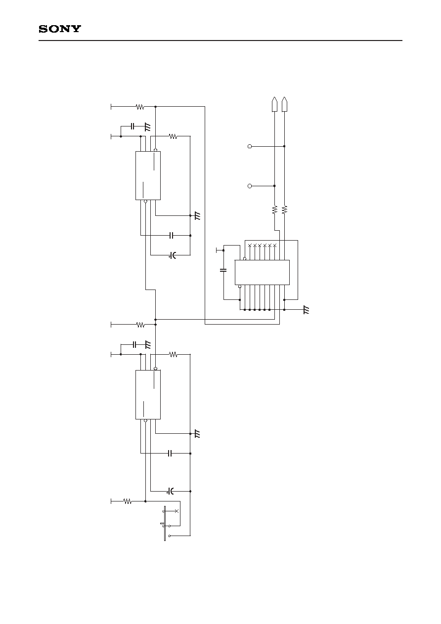
CXD4017R EVB Semiconductor Parts List
Parts No.
U1, 5
U2, 4
U3
U6
U7
U8
U9, 10, 11
U12, 13
U14
Q1
D1, 2, 9, 10
D3, 4, 11, 12
D5, 6, 13, 14
D7, 8, 15, 16
D17 to 22
Product name
NJM5532M
TC74HCT541F
AK4393VF
EP1K100QI208-2
EPC2LI20
CXD4017R
LM317T
TL7705CP
TC74LCX541F
2SC2223L
TLG124
TLY124
TLO124
TLR124
1S1588
Manufacturer
New Japan Radio
Toshiba
Asahi Kasei Microsystems
ALTERA
ALTERA
SONY
National Semiconductor
Texas Instruments
Toshiba
NEC
Toshiba
Toshiba
Toshiba
Toshiba
Toshiba
(15) Light emitting diode D16 is off when DTVALID is high, and lighted when DTVALID is low.
(16) Connection pins J3,J4, J7 and J9 are not used.
(17) Audio signal outputs LINE OUT and Headphone OUT are available. For headphone OUT, the output level
can be adjusted by RV1.
FPGA Operation
(1) Accumulates the number of error corrections, and displays.
(2) Detects the sampling frequency.
D9
D10
D11
D12
D13
D14
D15
Lighted with 1 error correction or more
Lighted with 3 error corrections or more
Lighted with 9 error corrections or more
Lighted with 27 error corrections or more
Lighted with 81 error corrections or more
Lighted with 243 error corrections or more
Lighted with 729 error corrections or more
(14) Light emitting diodes D9 to D15 display the number of error corrections. This is the total error correction
numbers during time for 48 chapters. The relationship between lighting of light emitting diodes and the
number of error corrections is shown in the table below.

≠ 24 ≠
CXD4017R
Circuit Diagram
POWER
MAIN1
LRCK0
BCK1
DAOUT0
APX1
DIF0
DIF1
DIF2
DEM0
DEM1
SMUTE
PDX
XRSTPW1
DTVALID
SWDIF0
LRCK1
BCK0
DAOUT1
CLK
EMPFS0
EMPFS1
SWDIF1
DTSEL
SCMODE
SRDT
CSOD
SWDT
XSCEN
SCLK
SWDIVCODE
SWCHNUM
DIVCODE
APX0
XRSTPW2
DFS
AUDIO
LRCK1
BCK1
DAOUT1
APX1
DIF0
DIF1
DIF2
DEM0
DEM1
SMUTE
PDX
DFS
RF
ADVIN
DIVCODE
MAIN2
LRCK0
BCK0
DAOUT0
DTVALID
XRSTPW2
ADVIN
SWDIF1
DTSEL
CLK
EMPFS1
EMPFS0
SWDIF0
SCMODE
SRDT
CSOD
SWDT
XSCEN
SCLK
SWDIVCODE
SWCHNUM
APX0
PWXRST
XRSTPW2
XRSTPW1
CXD4017R EVB Circuit Diagram (TOP)

≠ 25 ≠
CXD4017R
Rch (RED)
Lch (WHITE)
≠A5V
+A5V
+A5V
≠A5V
+A5V
+D5V
+D5V
D2.5V
R4
1k
U5A
NJM5532M
3
2
1
8
4
U5B
NJM5532M
5
6
7
8
4
R5
1k
R22
1k
R16
1k
R28
4.7k
R7
1k
R23
1k
C18
1000p
C20
3300p
R25
100
R3
1k
R6
1k
C3
1000p
R8
47k
R12
4.7k
R17
1k
R27
47k
C4
3300p
R18
1k
R24
47k
R11
47k
R9
100
R1
470
R2
470
U1B
NJM5532M
5
6
7
8
4
C6
1000p
RV1B
20k
4
5
6
C24
10Ķ/16V
C1
470Ķ/10V
C7
0.1Ķ
U1A
NJM5532M
3
2
1
8
4
C2
0.1Ķ
RV1A
20k
1
2
3
R10
1k
C21
1000p
J1
RCA JACK 2P
1
2
3
C10
10Ķ/16V
C8
470Ķ/10V
R26
1k
C17
0.1Ķ
C19
470Ķ/10V
C23
470Ķ/10V
C22
0.1Ķ
R20
4.7k
R13
4.7k
C14
10Ķ/16V
U4
74HCT541F
2
3
4
5
6
7
8
9
1
19
18
17
16
15
14
13
12
11
20
10
A1
A2
A3
A4
A5
A6
A7
A8
G1
G2
Y1
Y2
Y3
Y4
Y5
Y6
Y7
Y8
V
CC
GND
U3
AK4393VF
1
2
3
4
5
6
7
8
9
10
11
12
13
14
15
16
17
18
19
20
21
22
23
24
25
26
27
28
DV
SS
DV
DD
MCLK
PD
BICK
SDATA
LRCK
SMUTE
DFS
DEM0
DEM1
DIF0
DIF1
DIF2
BV
SS
VREFL
VREFH
AV
DD
AV
SS
AOUTR≠
AOUTR+
AOUTL≠
AOUTL+
VCOM
P/S
CKS0
CKS1
CKS2
C9
0.1Ķ
U2
74HCT541F
2
3
4
5
6
7
8
9
1
19
18
17
16
15
14
13
12
11
20
10
A1
A2
A3
A4
A5
A6
A7
A8
G1
G2
Y1
Y2
Y3
Y4
Y5
Y6
Y7
Y8
V
CC
GND
C12
0.1Ķ
C16
10Ķ/16V
C15
0.1Ķ
R15
4.7k
C11
10Ķ/16V
C5
0.1Ķ
R21
4.7k
C13
0.1Ķ
R14
4.7k
J2
PHONEJACK STEREO
3
2
1
R19
4.7k
DEM1
DIF0
LRCK1
BCK1
DIF2
DEM0
DAOUT1
APX1
DIF1
DFS
PDX
SMUTE
CXD4017R EVB Circuit Diagram (AUDIO)

≠ 26 ≠
CXD4017R
ON
ON
IFdata1
IFdata3
IFdata5
IFdata4
IFdata2
IFdata10
IFdata9
IFdata8
IFdata7
IFdata6
LED2
LED1
LED10
LED12
LED11
LED9
LED6
LED8
LED7
LED5
LED2
LED4
LED3
LED1
LED14
LED16
LED15
LED13
IFdata5
IFdata4
IFdata3
IFdata2
IFdata1
IFdata8
IFdata10
IFdata7
IFdata6
IFdata9
LED3
LED4
LED5
LED6
LED7
LED8
LED10
LED11
LED12
LED13
LED14
LED15
LED16
LED9
DSW2_8
DSW2_7
DSW2_6
DSW2_5
DSW2_4
DSW2_3
DSW2_2
DSW2_1
DSW1_1
DSW1_2
DSW1_4
DSW1_3
DSW1_2
DSW1_7
DSW1_1
DSW1_5
DSW1_8
DSW1_6
DSW1_3
DSW1_4
DSW1_5
DSW1_6
DSW1_7
DSW1_8
DSW2_1
DSW2_2
DSW2_3
DSW2_4
DSW2_5
DSW2_6
DSW2_7
DSW2_8
ALT3.3V
ALT3.3V
ALT3.3V
ALT3.3V
D2.5V
D2.5V
D2.5V
ALT3.3V
D2.5V
D2.5V
C50
0.1Ķ
RA3
M5-1-102J
1
2
3
4
5
COM
R1
R2
R3
R4
J5
XG4C-1031
1
3
2
4
5
6
7
8
9
10
TCK
TDO
GND
Vcc
TMS NC
NC
NC
TDI GND
C25
0.1Ķ
C48
0.1Ķ
C51
0.1Ķ
J4
IL-10P-S3EN2
1
2
3
4
5
6
7
8
9
10
A1
GND
A3
GND
A5
GND
A7
GND
A9
GND
C47
0.1Ķ
C26
0.1Ķ
C43
0.1Ķ
C38
0.1Ķ
C39
0.1Ķ
C31
0.1Ķ
C46
0.1Ķ
C37
0.1Ķ
C33
0.1Ķ
C45
0.1Ķ
C30
0.1Ķ
C28
0.1Ķ
C32
0.1Ķ
C34
0.1Ķ
C36
0.1Ķ
C27
0.1Ķ
C40
0.1Ķ
C35
0.1Ķ
C42
0.1Ķ
C29
0.1Ķ
C41
0.1Ķ
C44
0.1Ķ
TH11
TH
TH10
TH
TH8
TH
TH7
TH
TH1
TH
TH2
TH
TH4
TH
TH3
TH
TH6
TH
TH5
TH
C49
0.1Ķ
TH12
TH
TH14
TH
TH15
TH
TH13
TH
D5
TLO124
STA_5
D6
TLO124
STA_6
D7
TLR124
STA_7
D8
TLR124
STA_8
R70
1k
R30
1k
R29
10k
R61
10k
R38
100
R33
100
R35
100
R31
22
R39
100
R34
100
R42
100
R43
100
R50
100
R51
100
R52
100
R57
100
R58
100
R59
100
R60
100
R32
100
TP10
LC-2S-BK
DGND
1
TP11
LC-2S-BK
DGND
1
U7
EPC2LI20
1
2
3
4
5
6
7
8
9
10
11
12
13
14
15
16
17
18
19
20
TDO
DATA
TCK
DCLK
V
CC
SEL
NC
NC
OE
nCS
GND
TDI
nCASC
nInt_Conf
VppSel
NC
NC
NC
VPP
TMS
V
CC
S2
A6E-8104
1
2
3
4
5
6
7
8
16
15
14
13
12
11
10
9
R53
100
R54
100
R55
100
R56
100
D13
TLO124
STA_13
D14
TLO124
STA_14
D15
TLR124
STA_15
D16
TLR124
STA_16
R66
100
R67
100
R68
100
R69
100
R63
100
R64
100
D12
TLY124
STA_12
D9
TLG124A
STA_9
R62
100
D10
TLG124A
STA_10
R65
100
D11
TLY124
STA_11
D4
TLY124
Fs_0
D3
TLY124
Fs_1
D1
TLG124A
FULL/HALF
D2
TLG124A
CHNM
R49
100
TH9
TH
R45
100
R47
100
R44
100
TP5
LC-2S-Y
APX1
1
TP4
LC-2S-Y
SCLK
1
RA5
M9-1-103J
1
2
3
4
5
6
7
8
9
COM
R1
R2
R3
R4
R5
R6
R7
R8
RA2
M9-1-103J
1
2
3
4
5
6
7
8
9
COM
R1
R2
R3
R4
R5
R6
R7
R8
J3
IL-10P-S3EN2
1
2
3
4
5
6
7
8
9
10
A1
GND
A3
GND
A5
GND
A7
GND
A9
GND
RA1
M9-1-103J
1
2
3
4
5
6
7
8
9
COM
R1
R2
R3
R4
R5
R6
R7
R8
R48
100
TP7
LC-2S-Y
LRCK1
1
TP9
LC-2S-Y
BCK1
1
TP6
LC-2S-Y
DAOUT1
1
S1
A6E-8104
1
2
3
4
5
6
7
8
16
15
14
13
12
11
10
9
RA4
M9-1-103J
1
2
3
4
5
6
7
8
9
COM
R1
R2
R3
R4
R5
R6
R7
R8
TP3
LC-2S-Y
SWDT
1
TP1
LC-2S-Y
SCMODE
1
R41
100
R37
100
R40
100
TP8
LC-2S-Y
DTSEL
1
R46
100
R36
100
TP2
LC-2S-Y
XSCEN
1
U6
EP1K100QI208-2_1
1
2
3
4
5
6
7
8
9
10
11
12
13
15
14
16
17
18
19
20
21
22
23
24
25
26
27
28
29
30
31
32
33
34
35
36
37
38
39
40
41
42
43
44
45
46
47
48
49
50
51
52
53
54
55
56
57
58
59
60
61
62
63
64
65
66
67
68
69
70
71
72
73
74
75
76
77
78
79
80
81
82
83
84
85
86
87
88
89
90
91
92
93
94
95
96
97
98
99
100
101
102
103
104
105
106
107
108
109
110
111
112
113
114
115
116
117
118
119
120
121
122
123
124
125
126
127
128
129
130
131
132
133
134
135
136
137
138
139
140
141
142
143
144
145
146
147
148
149
150
151
152
153
154
155
156
157
158
159
160
161
162
163
164
165
166
167
168
169
170
171
172
173
174
175
176
177
178
179
180
181
182
183
184
185
186
187
188
189
190
191
192
193
194
195
196
197
198
199
200
201
202
203
204
205
206
207
208
TCK
CONF_DONE
nCEO
TDO
V
CC
IO
GND
EMPFS1
I_O
EMPFS0
I_O
DTVALID
I_O
DAOUT0
LRCK0
I_O
BCK0
SCMODE
SCLK
INIT_DONE
GND
V
CC
INT
V
CC
IO
GND
XSCEN
I_O
SWDT
SRDT
CSOD
I_O
I_O
SWDIVCODE
GND
V
CC
INT
V
CC
IO
GND
SWCHNUM
DTSEL
I_O
SWDIF0
I_O
SWDIF1
V
CC
IO
GND
DIVCODE
DSW1_1
I_O
DSW1_2
V
CC
INT
GND
TMS
TRST
nSTATUS
I_O
I_O
DSW1_3
DSW1_4
DSW1_5
DSW1_6
GND
DSW1_7
DSW1_8
LOCK
DSW2_1
I_O
DSW2_2
V
CC
IO
DSW2_3
DSW2_4
DSW2_5
DSW2_6
RMCK
V
CC
INT
I_O
I_O
I_O
GND
V
CC
_CKLK
XRSTPW2
GlobalCLK1
Ded_Input
GND_CLK
GND
DSW2_7
V
CC
IO
DSW2_8
I_O
LED9
LED10
I_O
LED11
V
CC
INT
LED12
I_O
LED13
I_O
LED14
LED15
V
CC
IO
I_O
LED16
I_O
LED1
I_O
LED2
nCONFIG
V
CC
INT
MSEL1
MSEL0
GND
V
CC
IO
LED3
I_O
LED4
I_O
LED5
LED6
GND
V
CC
IO
I_O
LED7
I_O
LED8
GND
V
CC
INT
DIF2
DIF1
I_O
DIF0
GND
V
CC
INT
I_O
DEM1
I_O
DEM0
I_O
I_O
GND
V
CC
IO
DFS
SMUTE
I_O
I_O
LRCK1
DAOUT1
GND
V
CC
IO
I_O
BCK1
PDX
APX1
GND
V
CC
INT
TDI
nCE
DCLK
DATA0
I_O
I_O
I_O
I_O
I_O
I_O
I_O
I_O
V
CC
IO
I_O
IFdata1
IFdata2
I_O
IFdata3
GND
IFdata4
I_O
IFdata5
I_O
I_O
I_O
V
CC
IO
I_O
I_O
GND
Ded_Input
CLK
Ded_Input
V
CC
INT
I_O
I_O
GND
I_O
I_O
I_O
I_O
I_O
V
CC
IO
I_O
IFdata6
I_O
IFdata7
I_O
IFdata8
V
CC
INT
I_O
IFdata9
nRS
IFdata10
nWS
CS
nCS
XRSTPW1
DEM0
DEM1
PDX
DIF0
DIF1
DIF2
APX0
CLK
DAOUT0
SWCHNUM
SMUTE
SRDT
CSOD
XRSTPW2
DFS
APX1
DAOUT1
DTSEL
BCK1
LRCK1
EMPFS1
BCK0
LRCK0
EMPFS0
DTVALID
SCMODE
SWDIVCODE
DIVCODE
XSCEN
SWDIF1
SWDIF0
SCLK
SWDT
CXD4017R EVB Circuit Diagram (PLD)

≠ 27 ≠
CXD4017R
Surface
mount
Surface mount
Surface
mount
A1.5V
D2.5V
A2.5V
A2.5V
D2.5V
D1.5V
X1
12.288MHz
C64
0.1Ķ
R83
1k
R82
10k
C55
0.1Ķ
C56
10Ķ/16V
R78
27
C65
1Ķ/35V T
MSVA1V105M
C58
0.1Ķ
C63
0.1Ķ
C62
0.1Ķ
C57
8p
C61
0.1Ķ
C59
8p
C60
0.1Ķ
C52
0.1Ķ
U8
CXD4017R
Direct mount
1
2
3
4
5
6
7
8
9
10
11
12
13
14
15
16
17
18
19
20
22
23
24
25
26
27
28
29
30
31
32
33
34
35
36
37
38
39
40
41
42
43
44
45
46
47
48
49
50
51
52
53
54
55
56
57
58
59
60
61
62
63
64
21
C53
0.1Ķ
C54
0.1Ķ
TP20
LC-2S-BK
DGND
TP21
LC-2S-BK
DGND
TP22
LC-2S-BK
DGND
TP23
LC-2S-BK
DGND
1
1
1
1
VR1
100
1
3
2
TP24
LC-2S-Y
ADVRH
1
TP27
LC-2S-Y
PLREF
1
TP28
LC-2S-Y
PLVAR
1
R84
22
TP29
LC-2S-Y
APX0
1
TP25
LC-2S-Y
SRDT
1
TP26
LC-2S-Y
CSOD
1
R81
100
TP12
LC-2S-Y
SYMCLK
1
TP19
LC-2S-Y
CLK
1
TP18
LC-2S-Y
BCK0
1
TP17
LC-2S-Y
LRCK0
1
TP16
LC-2S-Y
DAOUT0
1
TP13
LC-2S-Y
BMPFS0
1
TP14
LC-2S-Y
BMPFS1
1
TP15
LC-2S-Y
DTVALID
1
R77
22
R75
100
R79
10k
R80
100
R76
100
R71
100
R72
100
R73
100
R74
100
TP42
LC-2S-Y
TXOUT/RINFO
1
ADVIN
CLK
BCK0
LRCK0
DAOUT0
DTVALID
APX0
SCMODE
XSCEN
XRSTPW2
DTSEL
SWDIF0
SWDIF1
SWCHNUM
SWDIVCODE
EMPFS1
EMPFS0
CSOD
SRDT
SWDT
SCLK
EXTCK
DIVCODE
VCOR
V
DDI
APX
CHNUM
V
DDE
APAVS
V
SS
APCPO
APVCI
PLVAR
APAVD
V
SS
TEST16
PLREF
TEST5
TEST7
TEST9
TEST10
TEST6
TEST8
V
DDE
LRCK
DTVALID
EMPFS1
DAOUT
EMPFS0
TEST11
TEST4
TEST2
TEST3
TEST1
TEST0
V
SS
OSCO
V
DDE
OSCI
SCMODE
V
SS
SCLK
XSCEN
SRDT
SWDT
CSOD
TEST12
TEST14
TEST13
V
DDE
V
SS
ADAVS
ADVRH
ADAVD
ADVRL
V
DDE
ADVIN
V
SS
XRST
DIFM1
DIFM0
TEST15
V
SS
V
DDI
BCK
CXD4017R EVB Circuit Diagram (MAIN)
≠ 28 ≠
CXD4017R
+D5V
+A5V
≠A5V
ALT3.3V
D2.5V
A2.5V
A1.5V
D1.5V
VR3
200
13
2
R88
240
U10
LM317
3
1
2
VIN
ADJ
VOUT
VR2
50
13
2
R87
100
D17
1S1588
R85
240
D18
1S1588
U9
LM317
3
1
2
VIN
ADJ
VOUT
VR4
200
1
1
3
2
U11
LM317
3
1
2
VIN
ADJ
VOUT
R91
240
L7
SN3-200
L4
SN3-200
L5
SN3-200
L8
SN3-200
L1
SN3-200
L2
SN3-200
L3
SN3-200
L6
SN3-200
D19
1S1588
D21
1S1588
D20
1S1588
D22
1S1588
TP31
LC-2S-Y
1
TP34
LC-2S-Y
1
1
TP30
LC-2S-Y
1
TP32
LC-2S-Y
1
TP36
LC-2S-Y
1
C91
0.1Ķ
C79
0.1Ķ
C66
0.1Ķ
C67
47Ķ/16V
C77
0.1Ķ
C78
47Ķ/16V
R89
560
C72
0.1Ķ
C71
0.1Ķ
C75
10Ķ/16V
C86
0.1Ķ
TP37
LC-2S-BK
AGND
C84
0.1Ķ
C80
47Ķ/16V
C81
47Ķ/16V
C89
47Ķ/16V
C92
10Ķ/16V
C90
47Ķ/16V
C74
10Ķ/16V
C87
47Ķ/16V
C69
0.1Ķ
C83
10Ķ/16V
R90
330
C73
47Ķ/16V
C88
0.1Ķ
C68
47Ķ/16V
C70
10Ķ/16V
C76
0.1Ķ
C93
0.1Ķ
C94
47Ķ/16V
R86
270
R92
220
C82
0.1Ķ
C85
47Ķ/16V
R93
33
TP33
LC-2S-BK
AGND
J6
IL-4P-S3EN2
1
2
3
4
TP35
LC-2S-Y
1
J7
IL-2P-S3EN2
1
2
JP2
JP1
JP3
CXD4017R EVB Circuit Diagram (POWER)
≠ 29 ≠
CXD4017R
td = 60ms
td = 60ms
+D5V
+D5V
+D5V
+D5V
+D5V
D2.5V
C98
0.1Ķ
U12
TL7705CP
1
2
3
4
5
6
7
8
Vref
RESIN
Ct
GND
RESET
RESET
VsSENSE
V
CC
SW1
AB-15AH
1
2
3
C95
0.1Ķ
C97
4.7Ķ/16V T
C100
0.1Ķ
U13
TL7705CP
1
2
3
4
5
6
7
8
Vref
RESIN
Ct
GND
RESET
RESET
VsSENSE
V
CC
C96
0.1Ķ
C99
4.7Ķ/16V T
C101
0.1Ķ
R94
10k
R95
10k
R97
10k
R96
10k
R98
10k
U14
TC74LCX541F
1
2
3
4
5
6
7
8
9
10
11
12
13
14
15
16
17
18
19
20
G1
A1
A2
A3
A4
A5
A6
A7
A8
GND Y8
Y7
Y6
Y5
Y4
Y3
Y2
Y1
G2
V
CC
TP38
LC-2S-Y
XRSTPW1
1
TP39
LC-2S-Y
XRSTPW2
1
R99
100
R100
100
XRSTPW1
XRSTPW2
CXD4017R EVB Circuit Diagram (RESET)

≠ 30 ≠
CXD4017R
A2.5V
+A5V
+A5V
+A5V
C105
0.1Ķ
J8
SMB
VR5
5k
1
3
2
C102
0.1Ķ
C103
10Ķ/16V
R101
4.7k
R103
4.7k
Q1
2SC2223L
C104
0.1Ķ
C106
0.1Ķ
R102
4.7k
R104
10k
R105
1k
J9
IL-3P-S3EN2
1
2
3
TP40
LC-2S-Y
ADVIN
1
TP41
LC-2S-BK
AGND
1
ADVIN
DIVCODE
CXD4017R EVB Circuit Diagram (RFIN)

≠ 31 ≠
CXD4017R
Pattern Diagram
CXD4017R EVB A Side Pattern Diagram
CXD4017R EVB B Side Pattern Diagram

≠ 32 ≠
CXD4017R
CXD4017R EVB GND Layer Pattern Diagram
CXD4017R EVB Power Supply Layer Pattern Diagram

≠ 33 ≠
CXD4017R
CXD4017R EVB A Side Silk Diagram
CXD4017R EVB B Side Silk Diagram

≠ 34 ≠
CXD4017R
Package Outline Unit: mm
Sony Corporation
LEAD PLATING SPECIFICATIONS
ITEM
LEAD MATERIAL
42 ALLOY
SOLDER COMPOSITION
Sn-2%Bi
PLATING THICKNESS
5-20Ķm
SPEC.
SONY CODE
JEITA CODE
JEDEC CODE
LQFP-64P-L023
P-LQFP64-10X10-0.5
PACKAGE MATERIAL
TERMINAL TREATMENT
TERMINAL MATERIAL
PACKAGE MASS
EPOXY RESIN
SOLDER PLATING
42 ALLOY
0.32g
PACKAGE STRUCTURE
64PIN LQFP (PLASTIC)
DETAIL A
A
1
16
17
32
33
48
49
64
1.5 ≠ 0.1
+ 0.2
0į to 8į
12.0 Ī 0.2
10.0 Ī 0.1
b
0.1 Ī 0.1
0.5
Ī
0.2
DETAIL B
0.145 Ī 0.055
0.5
0.08
M
0.25
0.6
Ī
0.15
0.20 Ī 0.05
0.08
S
S