 | –≠–Ľ–Ķ–ļ—ā—Ä–ĺ–Ĺ–Ĺ—č–Ļ –ļ–ĺ–ľ–Ņ–ĺ–Ĺ–Ķ–Ĺ—ā: PEB2054 | –°–ļ–į—á–į—ā—Ć:  PDF PDF  ZIP ZIP |
ICs for Communications
Extended PCM Interface Controller
EPIC
ģ
-1
PEB 2055 / PEF 2055
Versions A3
EPIC
ģ
-S
PEB 2054 / PEF 2054
Versions 1.0
User's Manual 02.97

Edition 02.97
This edition was realized using the software system FrameMaker
ģ
.
Published by Siemens AG,
Bereich Halbleiter, Marketing-
Kommunikation, BalanstraŖe 73,
81541 MŁnchen
©
Siemens AG 7/23/97.
All Rights Reserved.
Attention please!
As far as patents or other rights of third parties are concerned, liability is only assumed for components, not for applications, processes
and circuits implemented within components or assemblies.
The information describes the type of component and shall not be considered as assured characteristics.
Terms of delivery and rights to change design reserved.
For questions on technology, delivery and prices please contact the Semiconductor Group Offices in Germany or the Siemens Companies
and Representatives worldwide (see address list).
Due to technical requirements components may contain dangerous substances. For information on the types in question please contact
your nearest Siemens Office, Semiconductor Group.
Siemens AG is an approved CECC manufacturer.
Packing
Please use the recycling operators known to you. We can also help you ≠ get in touch with your nearest sales office. By agreement we
will take packing material back, if it is sorted. You must bear the costs of transport.
For packing material that is returned to us unsorted or which we are not obliged to accept, we shall have to invoice you for any costs in-
curred.
Components used in life-support devices or systems must be expressly authorized for such purpose!
Critical components
1
of the Semiconductor Group of Siemens AG, may only be used in life-support devices or systems
2
with the express
written approval of the Semiconductor Group of Siemens AG.
1 A critical component is a component used in a life-support device or system whose failure can reasonably be expected to cause the
failure of that life-support device or system, or to affect its safety or effectiveness of that device or system.
2 Life support devices or systems are intended (a) to be implanted in the human body, or (b) to support and/or maintain and sustain hu-
man life. If they fail, it is reasonable to assume that the health of the user may be endangered.
PEB 2055
PEF 2055
Revision History:
User's Manual 02.97
Previous Release:
Technical Manual 02.92 (Editorial Update)
Page (in
Previous
Release)
Page
(in User's
Manual)
Subjects (major changes since last revision)

PEB 2055
PEF 2055
Semiconductor Group
3
02.97
Table of Contents
Page
1
Overview . . . . . . . . . . . . . . . . . . . . . . . . . . . . . . . . . . . . . . . . . . . . . . . . . . . . .7
1.1
Features . . . . . . . . . . . . . . . . . . . . . . . . . . . . . . . . . . . . . . . . . . . . . . . . . . . . . .8
1.2
Pin Configuration . . . . . . . . . . . . . . . . . . . . . . . . . . . . . . . . . . . . . . . . . . . . . . .9
1.3
Pin Definitions and Functions . . . . . . . . . . . . . . . . . . . . . . . . . . . . . . . . . . . .11
1.4
Logic Symbols . . . . . . . . . . . . . . . . . . . . . . . . . . . . . . . . . . . . . . . . . . . . . . . .14
1.5
Functional Block Diagram . . . . . . . . . . . . . . . . . . . . . . . . . . . . . . . . . . . . . . .16
1.6
Using the EPIC-S . . . . . . . . . . . . . . . . . . . . . . . . . . . . . . . . . . . . . . . . . . . . . .17
1.7
System Integration and Application . . . . . . . . . . . . . . . . . . . . . . . . . . . . . . . .18
1.7.1
Digital Line Card . . . . . . . . . . . . . . . . . . . . . . . . . . . . . . . . . . . . . . . . . . . . . .18
1.7.1.1 Switching, Layer-1 Control . . . . . . . . . . . . . . . . . . . . . . . . . . . . . . . . . . . . . . .18
1.7.1.2 Decentralized D-Channel Handling . . . . . . . . . . . . . . . . . . . . . . . . . . . . . . . .18
1.7.1.3 Central D-Channel Processing . . . . . . . . . . . . . . . . . . . . . . . . . . . . . . . . . . . .20
1.7.1.4 Mixed D-Channel Processing, Signaling Decentralized,
Packet Data Centralized
21
1.7.2
Analog Line Card . . . . . . . . . . . . . . . . . . . . . . . . . . . . . . . . . . . . . . . . . . . . . .23
1.7.3
Packet Handlers . . . . . . . . . . . . . . . . . . . . . . . . . . . . . . . . . . . . . . . . . . . . . . .24
2
Functional Description . . . . . . . . . . . . . . . . . . . . . . . . . . . . . . . . . . . . . . . .27
2.1
Bus Interface . . . . . . . . . . . . . . . . . . . . . . . . . . . . . . . . . . . . . . . . . . . . . . . . .27
2.2
PCM Interface . . . . . . . . . . . . . . . . . . . . . . . . . . . . . . . . . . . . . . . . . . . . . . . .28
2.3
Configurable Interface . . . . . . . . . . . . . . . . . . . . . . . . . . . . . . . . . . . . . . . . . .29
2.4
Memory Structure and Switching . . . . . . . . . . . . . . . . . . . . . . . . . . . . . . . . . .29
2.5
Pre-processed Channels, Layer-1 Support . . . . . . . . . . . . . . . . . . . . . . . . . .31
2.6
Special Functions . . . . . . . . . . . . . . . . . . . . . . . . . . . . . . . . . . . . . . . . . . . . . .31
3
Operational Description . . . . . . . . . . . . . . . . . . . . . . . . . . . . . . . . . . . . . . .32
3.1
Microprocessor Interface Operation . . . . . . . . . . . . . . . . . . . . . . . . . . . . . . . .32
3.2
Clocking . . . . . . . . . . . . . . . . . . . . . . . . . . . . . . . . . . . . . . . . . . . . . . . . . . . . .33
3.3
Reset . . . . . . . . . . . . . . . . . . . . . . . . . . . . . . . . . . . . . . . . . . . . . . . . . . . . . . .33
3.4
EPIC
ģ
Operation . . . . . . . . . . . . . . . . . . . . . . . . . . . . . . . . . . . . . . . . . . . . . .34
3.4.1
PCM-Interface . . . . . . . . . . . . . . . . . . . . . . . . . . . . . . . . . . . . . . . . . . . . . . . .35
3.4.2
Configurable Interface . . . . . . . . . . . . . . . . . . . . . . . . . . . . . . . . . . . . . . . . . .36
3.4.3
Switching Functions . . . . . . . . . . . . . . . . . . . . . . . . . . . . . . . . . . . . . . . . . . . .38
3.4.4
Special Functions . . . . . . . . . . . . . . . . . . . . . . . . . . . . . . . . . . . . . . . . . . . . . .41
3.5
Initialization Procedure . . . . . . . . . . . . . . . . . . . . . . . . . . . . . . . . . . . . . . . . . .42
3.5.1
Hardware Reset . . . . . . . . . . . . . . . . . . . . . . . . . . . . . . . . . . . . . . . . . . . . . . .42
3.5.2
EPIC
ģ
Initialization . . . . . . . . . . . . . . . . . . . . . . . . . . . . . . . . . . . . . . . . . . . . .42
3.5.2.1 Register Initialization . . . . . . . . . . . . . . . . . . . . . . . . . . . . . . . . . . . . . . . . . . .42
3.5.2.2 Control Memory Reset . . . . . . . . . . . . . . . . . . . . . . . . . . . . . . . . . . . . . . . . . .42
3.5.2.3 Initialization of Pre-processed Channels . . . . . . . . . . . . . . . . . . . . . . . . . . . .43
3.5.2.4 Initialization of the Upstream Data Memory (DM) Tristate Field . . . . . . . . . .45
3.5.3
Activation of the PCM and CFI Interfaces . . . . . . . . . . . . . . . . . . . . . . . . . . .45

PEB 2055
PEF 2055
Semiconductor Group
4
02.97
Table of Contents
Page
4
Detailed Register Description . . . . . . . . . . . . . . . . . . . . . . . . . . . . . . . . . . .46
4.1
Register Address Arrangement . . . . . . . . . . . . . . . . . . . . . . . . . . . . . . . . . . .46
4.2
Detailed Register Description . . . . . . . . . . . . . . . . . . . . . . . . . . . . . . . . . . . . .48
4.2.1
PCM Interface Registers . . . . . . . . . . . . . . . . . . . . . . . . . . . . . . . . . . . . . . . .48
4.2.1.1 PCM-Mode Register (PMOD) . . . . . . . . . . . . . . . . . . . . . . . . . . . . . . . . . . . .48
4.2.1.2 Bit Number per PCM-Frame (PBNR) . . . . . . . . . . . . . . . . . . . . . . . . . . . . . . .50
4.2.1.3 PCM-Offset Downstream Register (POFD) . . . . . . . . . . . . . . . . . . . . . . . . . .50
4.2.1.4 PCM-Offset Upstream Register (POFU) . . . . . . . . . . . . . . . . . . . . . . . . . . . .51
4.2.1.5 PCM-Clock Shift Register (PCSR) . . . . . . . . . . . . . . . . . . . . . . . . . . . . . . . . .51
4.2.1.6 PCM-Input Comparison Mismatch (PICM) . . . . . . . . . . . . . . . . . . . . . . . . . . .52
4.2.2
Configurable Interface Registers . . . . . . . . . . . . . . . . . . . . . . . . . . . . . . . . . .53
4.2.2.1 Configurable Interface Mode Register 1 (CMD1) . . . . . . . . . . . . . . . . . . . . . .53
4.2.2.2 Configurable Interface Mode Register 2 (CMD2) . . . . . . . . . . . . . . . . . . . . . .55
4.2.2.3 Configurable Interface Bit Number Register (CBNR) . . . . . . . . . . . . . . . . . . .58
4.2.2.4 Configurable Interface Time Slot Adjustment Register (CTAR) . . . . . . . . . . .58
4.2.2.5 Configurable Interface Bit Shift Register (CBSR) . . . . . . . . . . . . . . . . . . . . . .59
4.2.2.6 Configurable Interface Subchannel Register (CSCR) . . . . . . . . . . . . . . . . . .60
4.2.3
Memory Access Registers . . . . . . . . . . . . . . . . . . . . . . . . . . . . . . . . . . . . . . .61
4.2.3.1 Memory Access Control Register (MACR) . . . . . . . . . . . . . . . . . . . . . . . . . . .61
4.2.3.2 Memory Access Address Register (MAAR) . . . . . . . . . . . . . . . . . . . . . . . . . .65
4.2.3.3 Memory Access Data Register (MADR) . . . . . . . . . . . . . . . . . . . . . . . . . . . . .66
4.2.4
Synchronous Transfer Registers . . . . . . . . . . . . . . . . . . . . . . . . . . . . . . . . . .67
4.2.4.1 Synchronous Transfer Data Register (STDA) . . . . . . . . . . . . . . . . . . . . . . . .67
4.2.4.2 Synchronous Transfer Data Register B (STDB) . . . . . . . . . . . . . . . . . . . . . .67
4.2.4.3 Synchronous Transfer Receive Address Register A (SARA) . . . . . . . . . . . . .68
4.2.4.4 Synchronous Transfer Receive Address Register B (SARB) . . . . . . . . . . . . .69
4.2.4.5 Synchronous Transfer Transmit Address Register A (SAXA) . . . . . . . . . . . .69
4.2.4.6 Synchronous Transfer Transmit Address Register B (SAXB) . . . . . . . . . . . .70
4.2.4.7 Synchronous Transfer Control Register (STCR) . . . . . . . . . . . . . . . . . . . . . .70
4.2.5
Monitor/Feature Control Registers . . . . . . . . . . . . . . . . . . . . . . . . . . . . . . . . .71
4.2.5.1 MF-Channel Active Indication Register (MFAIR) . . . . . . . . . . . . . . . . . . . . . .71
4.2.5.2 MF-Channel Subscriber Address Register (MFSAR) . . . . . . . . . . . . . . . . . . .72
4.2.5.3 Monitor/Feature Control Channel FIFO (MFFIFO) . . . . . . . . . . . . . . . . . . . . .73
4.2.6
Status/Control Registers . . . . . . . . . . . . . . . . . . . . . . . . . . . . . . . . . . . . . . . .73
4.2.6.1 Signaling FIFO (CIFIFO) . . . . . . . . . . . . . . . . . . . . . . . . . . . . . . . . . . . . . . . .73
4.2.6.2 Timer Register (TIMR) . . . . . . . . . . . . . . . . . . . . . . . . . . . . . . . . . . . . . . . . . .74
4.2.6.3 Status Register (STAR) . . . . . . . . . . . . . . . . . . . . . . . . . . . . . . . . . . . . . . . . .75
4.2.6.4 Command Register (CMDR) . . . . . . . . . . . . . . . . . . . . . . . . . . . . . . . . . . . . .76
4.2.6.5 Interrupt Status Register (ISTA) . . . . . . . . . . . . . . . . . . . . . . . . . . . . . . . . . . .78
4.2.6.6 Mask Register (MASK) . . . . . . . . . . . . . . . . . . . . . . . . . . . . . . . . . . . . . . . . . .79
4.2.6.7 Operation Mode Register (OMDR) . . . . . . . . . . . . . . . . . . . . . . . . . . . . . . . . .80

PEB 2055
PEF 2055
Semiconductor Group
5
02.97
Table of Contents
Page
4.2.6.8 Version Number Status Register (VNSR) . . . . . . . . . . . . . . . . . . . . . . . . . . .82
5
Application Hints . . . . . . . . . . . . . . . . . . . . . . . . . . . . . . . . . . . . . . . . . . . . .83
5.1
Introduction . . . . . . . . . . . . . . . . . . . . . . . . . . . . . . . . . . . . . . . . . . . . . . . . . .83
5.1.1
IOM
ģ
and SLD Functions . . . . . . . . . . . . . . . . . . . . . . . . . . . . . . . . . . . . . . . .83
5.2
Configuration of Interfaces . . . . . . . . . . . . . . . . . . . . . . . . . . . . . . . . . . . . . . .89
5.2.1
PCM Interface Configuration . . . . . . . . . . . . . . . . . . . . . . . . . . . . . . . . . . . . .89
5.2.1.1 PCM Interface Signals . . . . . . . . . . . . . . . . . . . . . . . . . . . . . . . . . . . . . . . . . .89
5.2.1.2 PCM Interface Registers . . . . . . . . . . . . . . . . . . . . . . . . . . . . . . . . . . . . . . . .89
5.2.1.3 PCM Interface Characteristics . . . . . . . . . . . . . . . . . . . . . . . . . . . . . . . . . . . .91
5.2.2
Configurable Interface Configuration . . . . . . . . . . . . . . . . . . . . . . . . . . . . . .102
5.2.2.1 CFI Interface Signals . . . . . . . . . . . . . . . . . . . . . . . . . . . . . . . . . . . . . . . . . .102
5.2.2.2 CFI Registers . . . . . . . . . . . . . . . . . . . . . . . . . . . . . . . . . . . . . . . . . . . . . . . .102
5.2.2.3 CFI Characteristics . . . . . . . . . . . . . . . . . . . . . . . . . . . . . . . . . . . . . . . . . . .104
5.3
Data and Control Memories . . . . . . . . . . . . . . . . . . . . . . . . . . . . . . . . . . . . .130
5.3.1
Memory Structure . . . . . . . . . . . . . . . . . . . . . . . . . . . . . . . . . . . . . . . . . . . .130
5.3.2
Indirect Register Access . . . . . . . . . . . . . . . . . . . . . . . . . . . . . . . . . . . . . . .131
5.3.3
Memory Access Commands . . . . . . . . . . . . . . . . . . . . . . . . . . . . . . . . . . . .135
5.3.3.1 Access to the Data Memory Data Field . . . . . . . . . . . . . . . . . . . . . . . . . . . .135
5.3.3.2 Access to the Data Memory Code (Tristate) Field . . . . . . . . . . . . . . . . . . . .139
5.3.3.3 Access to the Control Memory Data Field . . . . . . . . . . . . . . . . . . . . . . . . . .142
5.3.3.4 Access to the Control Memory Code Field . . . . . . . . . . . . . . . . . . . . . . . . . .144
5.4
Switched Channels . . . . . . . . . . . . . . . . . . . . . . . . . . . . . . . . . . . . . . . . . . .151
5.4.1
CFI - PCM Time Slot Assignment . . . . . . . . . . . . . . . . . . . . . . . . . . . . . . . .152
5.4.2
Subchannel Switching . . . . . . . . . . . . . . . . . . . . . . . . . . . . . . . . . . . . . . . . .156
5.4.3
Loops . . . . . . . . . . . . . . . . . . . . . . . . . . . . . . . . . . . . . . . . . . . . . . . . . . . . . .161
5.4.3.1 CFI - CFI Loops . . . . . . . . . . . . . . . . . . . . . . . . . . . . . . . . . . . . . . . . . . . . . .161
5.4.3.2 PCM - PCM Loops . . . . . . . . . . . . . . . . . . . . . . . . . . . . . . . . . . . . . . . . . . . .164
5.4.4
Switching Delays . . . . . . . . . . . . . . . . . . . . . . . . . . . . . . . . . . . . . . . . . . . . .166
5.4.4.1 Internal Procedures at the Serial Interfaces . . . . . . . . . . . . . . . . . . . . . . . . .167
5.4.4.2 How to Determine the Delay . . . . . . . . . . . . . . . . . . . . . . . . . . . . . . . . . . . .170
5.4.4.3 Example: Switching of Wide Band ISDN Channels with the EPIC
ģ
. . . . . . .172
5.5
Preprocessed Channels . . . . . . . . . . . . . . . . . . . . . . . . . . . . . . . . . . . . . . . .175
5.5.1
Initialization of Preprocessed Channels . . . . . . . . . . . . . . . . . . . . . . . . . . . .176
5.5.2
Control/Signaling (CS) Handler . . . . . . . . . . . . . . . . . . . . . . . . . . . . . . . . . .187
5.5.2.1 Registers used in Conjunction with the CS Handler . . . . . . . . . . . . . . . . . .188
5.5.2.2 Access to Downstream C/I and SIG Channels . . . . . . . . . . . . . . . . . . . . . .190
5.5.2.3 Access to the Upstream C/I and SIG Channels . . . . . . . . . . . . . . . . . . . . . .191
5.5.3
Monitor/Feature Control (MF) Handler . . . . . . . . . . . . . . . . . . . . . . . . . . . . .193
5.5.3.1 Registers used in Conjunction with the MF Handler . . . . . . . . . . . . . . . . . .195
5.5.3.2 Description of the MF Channel Commands . . . . . . . . . . . . . . . . . . . . . . . . .200
5.6
Ķ
P Channels . . . . . . . . . . . . . . . . . . . . . . . . . . . . . . . . . . . . . . . . . . . . . . . .208

PEB 2055
PEF 2055
Semiconductor Group
6
02.97
Table of Contents
Page
5.7
Synchronous Transfer Utility . . . . . . . . . . . . . . . . . . . . . . . . . . . . . . . . . . . .212
5.7.1
Registers Used in Conjunction with the Synchronous Transfer Utility . . . . .215
5.8
Supervision Functions . . . . . . . . . . . . . . . . . . . . . . . . . . . . . . . . . . . . . . . . .221
5.8.1
Hardware Timer . . . . . . . . . . . . . . . . . . . . . . . . . . . . . . . . . . . . . . . . . . . . . .221
5.8.2
PCM Input Comparison . . . . . . . . . . . . . . . . . . . . . . . . . . . . . . . . . . . . . . . .223
5.8.3
PCM Framing Supervision . . . . . . . . . . . . . . . . . . . . . . . . . . . . . . . . . . . . . .226
5.8.4
Power and Clock Supply Supervision/Chip Version . . . . . . . . . . . . . . . . . . .227
5.9
Applications . . . . . . . . . . . . . . . . . . . . . . . . . . . . . . . . . . . . . . . . . . . . . . . . .228
5.9.1
Analog IOM
ģ
-2 Line Card with SICOFI
ģ
-4 as Codec/Filter Device . . . . . . .228
5.9.2
IOM
ģ
-2 Trunk Line Applications . . . . . . . . . . . . . . . . . . . . . . . . . . . . . . . . . .232
5.9.2.1 PBX With Multiple ISDN Trunk Lines . . . . . . . . . . . . . . . . . . . . . . . . . . . . . .233
5.9.2.2 Small PBX . . . . . . . . . . . . . . . . . . . . . . . . . . . . . . . . . . . . . . . . . . . . . . . . . .238
5.9.3
Miscellaneous . . . . . . . . . . . . . . . . . . . . . . . . . . . . . . . . . . . . . . . . . . . . . . .240
5.9.3.1 Interfacing the EPIC
ģ
to a MUSAC
TM
. . . . . . . . . . . . . . . . . . . . . . . . . . . . . .240
5.9.3.2 Space and Time Switch for 16 kbit/s Channels . . . . . . . . . . . . . . . . . . . . . .242
5.9.3.3 Interfacing an IOM
ģ
-2 Terminal Mode Interface
to a 2.048 Mbit/s PCM Backplane . . . . . . . . . . . . . . . . . . . . . . . . . . . . . . . .244
6
Electrical Characteristics . . . . . . . . . . . . . . . . . . . . . . . . . . . . . . . . . . . . .246
7
Package Outlines . . . . . . . . . . . . . . . . . . . . . . . . . . . . . . . . . . . . . . . . . . . .257
8
Appendix . . . . . . . . . . . . . . . . . . . . . . . . . . . . . . . . . . . . . . . . . . . . . . . . . . .258
8.1
Working Sheets . . . . . . . . . . . . . . . . . . . . . . . . . . . . . . . . . . . . . . . . . . . . . .258
8.1.1
Register Summary for EPIC
ģ
Initialization . . . . . . . . . . . . . . . . . . . . . . . . . .258
8.1.2
Switching of PCM Time Slots to the CFI Interface (data downstream) . . . .262
8.1.3
Switching of CFI Time Slots to the PCM Interface (data upstream) . . . . . . .263
8.1.4
Preparing EPIC
ģ
s C/I Channels . . . . . . . . . . . . . . . . . . . . . . . . . . . . . . . . . .264
8.1.5
Receiving and Transmitting IOM
ģ
-2 C/I-Codes . . . . . . . . . . . . . . . . . . . . . .265
8.2
Development Tools . . . . . . . . . . . . . . . . . . . . . . . . . . . . . . . . . . . . . . . . . . .266
8.2.1
SIPB 5000 Mainboard . . . . . . . . . . . . . . . . . . . . . . . . . . . . . . . . . . . . . . . . .266
8.2.2
SIPB 5121 IOM
ģ
-2 Line Card (EPIC
ģ
/IDEC
ģ
) . . . . . . . . . . . . . . . . . . . . . . .267
8.2.3
EPIC
ģ
Configurator . . . . . . . . . . . . . . . . . . . . . . . . . . . . . . . . . . . . . . . . . . .268
9
Lists . . . . . . . . . . . . . . . . . . . . . . . . . . . . . . . . . . . . . . . . . . . . . . . . . . . . . . .269
9.1
Glossary . . . . . . . . . . . . . . . . . . . . . . . . . . . . . . . . . . . . . . . . . . . . . . . . . . . .269
IOM
ģ
, IOM
ģ
-1, IOM
ģ
-2, SICOFI
ģ
, SICOFI
ģ
-2, SICOFI
ģ
-4, SICOFI
ģ
-4ĶC, SLICOFI
ģ
, ARCOFI
ģ
, ARCOFI
ģ
-BA,
ARCOFI
ģ
-SP, EPIC
ģ
-1, EPIC
ģ
-S, ELIC
ģ
, IPAT
ģ
-2, ITAC
ģ
, ISAC
ģ
-S, ISAC
ģ
-S TE, ISAC
ģ
-P, ISAC
ģ
-P TE, IDEC
ģ
,
SICAT
ģ
, OCTAT
ģ
-P, QUAT
ģ
-S are registered trademarks of Siemens AG.
MUSAC
TM
-A, FALC
TM
54, IWE
TM
, SARE
TM
, UTPT
TM
, ASM
TM
, ASP
TM
are trademarks of Siemens AG.
Purchase of Siemens
I
2
C components conveys a license under the Philips'
I
2
C patent to use the components in
the
I
2
C-system provided the system conforms to the
I
2
C specifications defined by Philips. Copyright Philips 1983.

PEB 2055
PEF 2055
Overview
Semiconductor Group
7
1
Overview
The PEB 2055 (Extended PCM Interface Controller) is a highly integrated controller
circuit optimized for analog and ISDN line card and central switches applications. The
EPIC-1 provides the circuitry necessary to manage up to 32 digital (ISDN or proprietary)
or 64 analog subscribers.
The EPIC-1 is dedicated to switch PCM data between two serial interfaces, the system
interface (PCM interface) and the configurable interface (CFI). The EPIC-1 performs
non-blocking time and space switching for up to 128 channels.
Since the system cost of the EPIC-1 is divided by the number of lines it controls, an
highly economical implementation of digital or analog subscriber lines can be performed.
The EPIC-S (PEB 2054) is a pin compatible device offering half the switching capacity
of the EPIC-1. Therefore the EPIC-S is capable of handling up to 16 ISDN or 32 analog
subscribers. It is programmable according to the EPIC-1 with respect of the pins not
available.
The EPIC is implemented in a Siemens advanced CMOS-technology and manufactured
in a P-LCC-44-1 package.
The EPIC is member of a chip family supporting a highly economical implementation of
line cards and subscriber terminals.
Chip Family
Line Cards:
PEB 2055
Extended PCM Interface Controller
(EPIC)
PEB 20550
Extended Line Card Controller
(ELIC)
PEB 2096
Octal U
PN
Transceiver
(OCTAT-P)
PEB 2095
ISDN Burst Transceiver Circuit
(IBC)
PEB 2084
Quadruple S
0
Transceiver
(QUAT-S)
PEB 2465
Quadruple DSP based Codec Filter
(SICOFI-4)
PEB 2075
ISDN D-Channel Exchange Controller
(IDEC)
Terminals:
PSB 2196
Digital Subscriber Access Controller
(ISAC-P TE)
for U
PN
Interface
PEB 2081 (V3.2)
S/T-Bus Interface Circuit Extended
(SBCX)

P-LCC-44-1
Semiconductor Group
8
02.97
Extended PCM Interface Controller
EPIC
ģ
-1, EPIC
ģ
-S
PEB 2055
PEF 2055
PEB 2054
PEF 2054
Versions A3 (PEB 2055), V1.0 (PEB 2054)
CMOS
Type
Ordering Code
Package
PEB 2055
Q67100-H6035
P-LCC-44-1
PEF 2055
Q67100-H6216
P-LCC-44-1
PEB 2054
Q67100-H6420
P-LCC-44-1
PEF 2054
Q67100-H6534-B701
P-LCC-44-1
1.1
Features
Switching
∑ Board Controller for up to
≠ 32 ISDN or 64 analog subscribers (PEB 2055)
≠ 16 ISDN or 32 analog subscribers (PEB 2054)
∑ Non-blocking switch for
≠ 128 channels (PEB 2055)
≠ 64 channels (PEB 2054)
∑ Switching of 16-, 32-, or 64-kbit/s channels
∑ Two consecutive 64-kbit/s channels can be switched as a single 128-kbit/s channel
∑ Freely programmable time slot assignment for all subscribers
∑ Two serial interfaces (PCM and CFI) programmable over a wide data range (128 -
8192 kbit/s)
∑ Data rates of PCM and configurable interface independent from each other (data rate
adaptation)
∑ PCM-interface
≠ Tristate control signals for external drivers
≠ Programmable clock shift
≠ Single or double data clock
∑ Configurable interface
≠ Configurable for IOM-, SLD- and PCM-applications
≠ High degree of flexibility for datastream adaptation
≠ Programmable clockshift
≠ Single or double data clock
∑ Synchronous
Ķ
P-access to two selected channels
PEB 2055
PEF 2055
Overview
Semiconductor Group
9
Handling of Layer-1 Functions
∑ Change detection for C/I-channel (IOM-configuration) or feature control
(SLD-configuration)
∑ Double last-look logic for C/I-channel (IOM-2 analog configuration)
∑ Additional last-look logic for feature control (SLD-configuration)
∑ Buffered monitor (IOM-configuration) or signaling channel (SLD-configuration)
Bus Interface
∑ Siemens/Intel or Motorola type
Ķ
P-interface
∑ 8-bit demultiplexed bus interface
∑ FIFO-access interrupt or DMA controlled
1.2
Pin Configuration
(top view)
Figure 1
Pin Configuration EPIC
ģ
-1
EPIC
ITP09463
6
5
4
3
2
1
44
43
42
41
40
7
8
9
10
11
12
13
14
15
16
17
28 27 26 25 24 23 22 21 20 19 18
39
38
37
36
35
34
33
32
31
30
29
PDC
WR
PFS
CS
TxD3
ALE
TSC3
INT
TxD2
DCL
TSC2
FSC
DU3/SIP7
TSC1
DU2/SIP6
TxD0
DU1/SIP5
TSC0
DU0/SIP4
A1
A3
DD0/SIP0
DD1/SIP1
DD2/SIP2
DD3/SIP3
RES
A0
RxD3
RxD2
RxD1
RxD0
DD
V
V
SS
DS/RD
AD6
AD5
AD4
AD3
AD2
AD1
AD0
A2
TxD1
AD7
PEB 2055
R/W,
R

PEB 2055
PEF 2055
Overview
Semiconductor Group
10
Figure 2
Pin Configuration EPIC
ģ
-S
ITP09530
6
5
4
3
2
1
44
43
42
41
40
7
8
9
10
11
12
13
14
15
16
17
28 27 26 25 24 23 22 21 20 19 18
39
38
37
36
35
34
33
32
31
30
29
PDC
WR
PFS
CS
TxD3
ALE
TSC3
INT
TxD2
DCL
TSC2
FSC
N.C.
TSC1
N.C.
TxD0
DU1
TSC0
DU0
A1
A3
DD0
DD1
N.C.
N.C.
RES
A0
RxD3
RxD2
RxD1
RxD0
DD
V
V
SS
DS/RD
AD6
AD5
AD4
AD3
AD2
AD1
AD0
A2
TxD1
AD7
R/W,
2054
PEB
-S
EPIC
R

PEB 2055
PEF 2055
Overview
Semiconductor Group
11
1.3
Pin Definitions and Functions
Pin No.
EPIC-S EPIC
Symbol Input (I)
Output (O)
Function
30
30
CS
I
Chip Select; active low. A "low" on this line
selects the EPIC for read/write operations.
29
29
WR,
R/W
I
Write, active low, Siemens/Intel bus mode.
When "low", a write operation is indicated.
Read/Write, Motorola bus mode.
When "high" a valid
Ķ
P-access identifies a read
operation, when "low" it identifies a write access.
28
28
RD, DS
I
Read, active low, Siemens/Intel bus mode.
When "low" a read operation is indicated.
Data Strobe, Motorola bus mode.
A rising edge marks the end of a read or write
operation.
19
20
21
22
23
24
25
26
19
20
21
22
23
24
25
26
AD0, D0
AD1, D1
AD2, D2
AD3, D3
AD4, D4
AD5, D5
AD6, D6
AD7, D7
I/O
I/O
I/O
I/O
I/O
I/O
I/O
I/O
Address/Data Bus; multiplexed bus mode.
Transfers addresses from the
Ķ
P-system to the
EPIC and data between the
Ķ
P and the EPIC.
Data Bus; demultiplexed bus mode.
Transfers data between the
Ķ
P and the EPIC.
When driving data the pins have push pull
characteristic, otherwise they are in high
impedance state.
31
31
ALE
I
Address Latch Enable
ALE controls the on chip address latch in
multiplexed bus mode. While ALE is "high", the
latch is transparent. The falling edge latches the
current address. During the first read/write
access following reset ALE is evaluated to select
the bus mode.
32
32
INT
O
(OD)
Interrupt Request, active low.
This signal is activated when the EPIC requests
an interrupt. Due to the open drain (OD)
characteristic of INT multiple interrupt sources
can be connected together.
44
44
RES
I
Reset
A "high" forces the EPIC into reset state.
16
16
PFS
I
PCM Interface Frames Synchronization

PEB 2055
PEF 2055
Overview
Semiconductor Group
12
17
17
PDC
I
PCM Interface Data Clock
Single or double data rate.
6
5
4
3
6
5
4
3
RxD0
RxD1
RxD2
RxD3
I
I
I
I
Receive PCM Interface Data
Time-slot oriented data is received on this pins
and forwarded into the downstream data memory
of the EPIC.
9
11
13
15
9
11
13
15
TxD0
TxD1
TxD2
TxD3
O
O
O
O
Transmit PCM Interface Data
Time slot oriented data is shifted out of the
EPIC's upstream data memory on this lines. For
time-slots which are flagged in the tristate
data memory or when bit OMDR:PSB is reset
the pins are set to high impedance state.
8
10
12
14
8
10
12
14
TSC0
TSC1
TSC2
TSC3
O
O
O
O
Tristate Control
Supplies a control signal for an external driver.
These lines are "low" when the corresponding
TxD outputs are valid. During reset these lines
are "high".
34
34
FSC
I/O
Frame Synchronization
Input or output in IOM configuration. Direction
indication signal in SLD mode.
33
33
DCL
I/O
Data Clock
Input or output in IOM, slave clock in SLD
configuration. In IOM configuration single or
double data rate, single data rate in SLD mode.
38
37
-
-
38
37
36 *
35 *
DU0/SIP4
DU1/SIP5
DU2/SIP6
DU3/SIP7
I/IO (OD)
I/IO (OD)
I/IO (OD)
I/IO (OD)
Data Upstream Input; IOM or PCM configuration.
Serial Interface Port, SLD configuration.
Depending on the bit OMDR:COS these lines
have push pull or open drain characteristic.
For unassigned channels or when bit
OMDR:CSB is reset the pins are in the state
high impedance.
* Note: EPIC-1 only
1.3
Pin Definitions and Functions (cont'd)
Pin No.
EPIC-S EPIC
Symbol Input (I)
Output (O)
Function

PEB 2055
PEF 2055
Overview
Semiconductor Group
13
40
41
-
-
40
41
42 *
43 *
DD0/SIP0
DD1/SIP1
DD2/SIP2
DD3/SIP3
O/IO (OD)
O/IO (OD)
O/IO (OD)
O/IO (OD)
Data Downstream Output, IOM or PCM
configuration.
Serial Interface Port, SLD configuration.
Depending on the bit OMDR:COS these lines
have push pull or open drain characteristic.
For unassigned channels or when bit
OMDR:CSB is reset the pins are in the high
impedance state.
* Note: EPIC-1 only
2
7
18
39
2
7
18
39
A0
A1
A2
A3
I/O
Address bus in the demultiplexed
Ķ
P interface
mode.
1
1
V
DD
I
Supply voltage: 5 V
Ī
5%
27
27
V
SS
I
Ground: 0 V
1.3
Pin Definitions and Functions (cont'd)
Pin No.
EPIC-S EPIC
Symbol Input (I)
Output (O)
Function

PEB 2055
PEF 2055
Overview
Semiconductor Group
14
1.4
Logic Symbols
Figure 3
Logic Symbol of the EPIC
ģ
-1
DCL
0
ITL09531
FSC
DU
DD
PFS
0
PDC
0
1
1
2
2
2
3
3
3
0
0
1
1
DD
DU
2
2
DD
DU
3
3
DD
DU
TxD
RxD
RxD
TxD
TxD
RxD
TxD
TSC
PCM
Port 0
1
PCM
PCM
2
PCM
3
CFI
Port 0
1
Port
CFI
2
Port
CFI
3
Port
CFI
TSC
TSC
TSC
EPIC -1
RxD 1
Port
Port
Port
AD7...0
A3...0
RD
WR
ALE
CS
INT
R

PEB 2055
PEF 2055
Overview
Semiconductor Group
15
Figure 4
Logic Symbol of the EPIC
ģ
-S
DCL
ITL09532
FSC
DU
DD
0
0
1
1
DD
DU
CFI
Port 0
1
Port
CFI
EPIC -S
R
RxD 3
TxD 1
3
3
2
2
2
TSC
TSC
TxD
RxD
1
RxD
TxD
TSC 1
0
PDC
0
PFS
0
RxD
TSC
TxD
Port
Port
PCM
3
2
Port
PCM
PCM
1
Port
PCM
0
RD
AD7...0
A3...0
WR
ALE
CS
INT

PEB 2055
PEF 2055
Overview
Semiconductor Group
16
1.5
Functional Block Diagram
Figure 5
Functional Block Diagram EPIC
ģ
DCL
ITB09533
FSC
DU
DD
DD
DU
DD
DU
DD
DU
AD7...0
A3...0
RD
WR
ALE CS INT
Timer
Data Memory
Control Memory
P Interface
RES
PDC
PFS
/ SCL
/ DIR
3
3
2
2
1
1
0
0
/ SIP 0
4
SIP
/
1
SIP
/
5
SIP
/
2
SIP
/
6
SIP
/
3
SIP
/
7
SIP
/
Configurable
Interface
Layer 1
Controller
Buffer
PCM Interface
RxD0
TxD0
TSC0
RxD1
TxD1
TSC1
RxD2
TxD2
TSC2
RxD3
TxD3
TSC3
Ķ

PEB 2055
PEF 2055
Overview
Semiconductor Group
17
1.6
Using the EPIC-S
The EPIC-S is based on the same technology as the EPIC-1 aside from only providing
CFI port 0 and CFI port 1. Therefore this User's Manual applies to both, the EPIC-S and
the EPIC-1.
When using the EPIC-S the user has to be aware not to program connections that would
imply the not supported CFI ports.
The following points require specific attention:
1. During power up the EPIC-S must be supplied with an external Hardware Reset.
2. Register bit OMDR:CSB may be programmed to high (switch off standby of CFI
interface) only after a Control Memory reset procedure with MACR:CMC3..0 = 0
H
.
3. The pins not available with respect to the EPIC-1 (PEB 2055) must not be
programmed as outputs.

PEB 2055
PEF 2055
Overview
Semiconductor Group
18
1.7
System Integration and Application
The main application fields of the EPIC are:
≠ Digital line cards with different architectures,
≠ Central control units of key systems,
≠ Analog line cards,
≠ Concentrators.
1.7.1
Digital Line Card
1.7.1.1 Switching, Layer-1 Control
The EPIC provides a switching capability for up to 32 digital subscribers between the
PCM system highway and the IOM-2 interface (64 B-channels). Typically it switches
64-kbit/s channels between the PCM and the IOM-interfaces. Moreover it is able to
handle also 16-, 32- and 128-kbit/s channels.
The signaling handler supports the command/indication (C/I) channel which is used to
exchange predefined layer-1 information with the transceiver device.
A monitor handler supports the handshake protocol defined on the IOM-monitor channel.
It allows programming of layer-1 devices which do not have a dedicated
Ķ
P interface.
The EPIC can be operated in tandem, i.e. one device is active, another one is a backup
device. The backup device can instantaneously take over from the active device when
the active device fails. Due to this tandem operation capability and the high number of
ISDN subscribers which can be connected to one EPIC, the use of single line cards is
feasible.
Several line card architectures are possible.
1.7.1.2 Decentralized D-Channel Handling
In completely decentral D-channel processing architectures (see figure 6), the
processing capacity of the line card is usually designed to avoid blocking situations even
under maximum conceivable D-channel traffic conditions. In such an architecture the
EPIC switches the B-channels and performs C/I and monitor channel control.
The IDECs handle the layer 2 functions for signaling and data packets in the D-channel.
They transfer the extracted data via the
Ķ
P and an HDLC controller, e.g. the HSCX (High
Level Serial Controller Extended SAB 82525) to the system. One of the channels of the
HSCX may access either a time slot of programmable bandwidth on one of the system
highways or a separate signalling highway.
In both cases the highway capacity used for packet traffic can be shared among several
line cards due to the statistical multiplexing capabilities of the HSCX.

PEB 2055
PEF 2055
Overview
Semiconductor Group
19
Figure 6
Line Card Architecture for Completely Decentral D-Channel Processing
ITS09534
P
Interface
s
Data
B
B
B
B
B
S
B
...
Example Frame Structure
p-Data
s-Data
s-Data
+ p
PCM
Packet Highway with
Collision Resolution
Highway
HSCX
Ķ
R
IOM -2
R
IDEC
IDEC
R
R
EPIC

PEB 2055
PEF 2055
Overview
Semiconductor Group
20
1.7.1.3 Central D-Channel Processing
In this application the EPIC not only switches the B-channels and performs the C/I- and
monitor channel control function, but switches also the D-channel data onto the system
highway. In upstream direction the EPIC can combine up to four 16-kbit/s D-channels
into one 64-kbit/s channel. In downstream direction it provides the capability to distribute
one 64-kbit/s channel to four 16-kbit/s channels.
Figure 7
Digital Line Card Architecture with a Completely Central D-Channel Handling
ITS09535
EPIC
Interface
B
B
B
B
...
Example Frame Structure
D
B,
D D D D
PCM
Highway
HSCX
P
Highway
Signaling
R
IOM -2
R
Ķ

PEB 2055
PEF 2055
Overview
Semiconductor Group
21
1.7.1.4 Mixed D-Channel Processing, Signaling Decentralized,
Packet Data Centralized
Another possibility is a mixed architecture with centralized packet data and decentralized
signaling handling. This is a very flexible architecture which reduces the dynamic load of
central processing units by evaluating the signaling information on the line card, but does
not require resources for packet data handling. Any increase of packet data traffic does
not necessitate a change in the line card architecture, the central packet handling unit
can be expanded.
In this application IDECs are employed to handle the data on the D-channel. The IDECs
separate signaling information from data packets. The signaling messages are
transferred to the
Ķ
P, which in turn hands them over to the group controller using the
HSCX.
The packet data is processed differently. Together with the collision resolution
information it is transferred to one IOM-2 port of the EPIC. The EPIC switches the
channels to the PCM-highway, optionally combining four D-channels to one 64-kbit/s
channel. In this configuration one IOM-2 interface is occupied by IDECs, reducing the
total switching capability of the EPIC-1 to 24 ISDN-subscribers.
Figure 8
Line Card Architecture for Mixed D-Channel Processing
ITS09536
Interface
Sig.
Data
B
B
B
P
B
C
B
...
Example Frame Structure
Signaling
S
PCM
Signaling
Highway
Highway
HSCX
Coll
+
P
p - Data
P
B, P, C
Packet
Data
Collision
Data
EPIC
R
R
IOM -2
Ķ
P
IDEC
R
IDEC
R

PEB 2055
PEF 2055
Overview
Semiconductor Group
22
Alternatively, the packet and collision data can be directly exchanged between the
IDECs and the PCM-highway. Thus, the full 32 subscriber switching capability of the
EPIC is retained.
Figure 9
Line Card Architecture for Mixed D-Channel Processing
ITS09537
Signaling
Highway
C
System
Highway
HSCX
B
PCM Interface
B, P
Coll
S
B, P
D
P
P
Coll
S
S
-2
IOM
R
Interface
Ķ
R
IDEC
EPIC
R

PEB 2055
PEF 2055
Overview
Semiconductor Group
23
1.7.2
Analog Line Card
Together with the highly flexible Siemens codec filter circuits SLICOFI, SICOFI,
SICOFI-2 or SICOFI-4 the EPIC constitutes an optimized analog subscriber board
architecture.
The EPIC-1 handles the signalling and voice data for up to 64 subscriber channels with
64 kbit/s. The HSCX establishes the link to the group controller board.
Figure 10
Line Card Architecture for Analog Subscribers
ITS09538
SICOFI -4
C/I, Monitor
Channel
P
PCM Highway
Signaling Highway
B Channels
HSCX
P
Ķ
R
IOM -2
IOM
R
-2
IOM
R
-2
IOM
R
-2
R
EPIC
R
SICOFI -4
R
SICOFI -4
R
SICOFI -4
R
SICOFI -4
R
SICOFI -4
R
SICOFI -4
R
SICOFI -4
R

PEB 2055
PEF 2055
Overview
Semiconductor Group
24
1.7.3
Packet Handlers
The EPIC is an important building block for networks based on either central, decentral
or mixed signaling and packet data handling architectures. Its flexibility allows for the
modification of the packet handling architecture according to the changing needs.
Thus it may be useful to add central packet handling groups to a network originally based
on decentral signaling and packet handling. This may be the case if growing data packet
traffic exceeds the initial capacity of the network. The result is a mixed architecture.
On the other hand, increasing packet handling demand on a few dedicated subscriber
lines calls for solutions which back up the capacity at these few decentral line cards.
In both of these cases and several other applications, the EPIC is a powerful device for
solving the problem of packet handling. In most applications it is used together with the
IDEC (ISDN D channel Exchange Controller).
Decentralized and mixed packet handling has already been covered in the line card
chapter. In the following, the centralized signaling/packet handlers built up with the EPIC
will be described.
Central packet handling is used if many subscribers with a generally low demand for
packet switching are to be connected to a system. Concentrating the packet servers for
multiple users eliminates the need to provide a packet server channel for every user. The
overall number of packet server channels can thus be reduced.
In such a central packet handling group, the EPIC performs the switching and
concentrator function. It connects a variable number of PCM highways to the packet
handler internal highway. HDLC controllers are also connected to this internal highway
as illustrated in figure 11.
Figure 11
Centralized Packet Handler with a Single Internal Highway Connected to 4 PCM
Highways
ITS09539
IDEC
Packet Handler Internal Highway
A
B
C
D
PCM Highways
Centralized Packet Handler Unit
R
R
IDEC
C
Ķ
EPIC
R

PEB 2055
PEF 2055
Overview
Semiconductor Group
25
This figure shows one EPIC connecting four PCM highways to one packet handler
internal highway. These highways are accessed by the IDECs, which are 4 channel
HDLC controller and handle the packets. If more than four PCM highways shall be
connected to the centralized packet handler, further EPICs are necessary. Such a
configuration is shown in figure 12, where 8 highways are switched to one packet
handler internal highway. In this case the two EPICs are connected in parallel at the
packet handlers internal side.
Figure 12
Centralized Packet Handler with One Internal Highway Connected to 8 PCM High-
ways
The data rate of the packet handler internal highway can be up to 4.096 Mbit/s. If this
capacity is not sufficient, other packet handler internal highways may be added as
depicted in figure 13.
ITS09540
E F G H
PCM Highways
Centralized Packet Handler Unit
Packet Handler Internal Highway
S
D
C
B
A
IDEC
R
IDEC
R
Ķ
C
R
EPIC
EPIC
R

PEB 2055
PEF 2055
Overview
Semiconductor Group
26
Figure 13
Centralized Packet Handler with 3 Internal Highways
In some applications an additional collision resolution signal is required for the HDLC
controllers. This information can be demultiplexed from the PCM highways to a third line
for each packet handler internal highway (refer to figure 14).
Figure 14
Centralized Packet Handler with Internal Collision Line
The applications apply equally to centralized signaling as well as to data packet
handlers.
ITS09541
E F G H
PCM Highways
Centralized Packet Handler Unit
Packet Handler Internal Highway
S
D
C
B
A
EPIC
R
EPIC
R
IDEC
R
IDEC
R
IDEC
R
C
Ķ
ITS09542
A
B
C
D
PCM Highways
Centralized Packet Handler Unit
Packet Handler Internal Highway
S
Collision
Indication
Line
R
EPIC
IDEC
R
IDEC
R
C
Ķ

PEB 2055
PEF 2055
Functional Description
Semiconductor Group
27
2
Functional Description
In the following chapters the functions of the PEB 2055 will be covered in more detail.
2.1
Bus Interface
All registers and the FIFOs of the EPIC are accessible via the flexible bus interface
supporting Siemens / Intel and Motorola type microprocessors. Depending on the
register functionality a read, write or read/write access is possible.
The bus interface consists of the following elements
∑ Data bus, 8-bit wide, D7 .. 0
∑ Address bus, 4-bit wide, A3 .. 0
∑ Chip select, CS
∑ Address latch enable, ALE
∑ Two read/write control lines: RD and WR (Intel mode) or DS and R/W (Motorola
mode)
∑ Interrupt, INT
∑ Reset, RES
The ALE line is used to control the bus structure and interface type.
Table 1
Selectable Bus Configurations
Figure 15
Selectable Bus Interface Structures
ALE
Interface
Bus Structure
Pin 28
Pin 29
Fixed to
V
DD
Motorola
demultiplexed
DS
R/W
Fixed to ground
Siemens / Intel
demultiplexed
RD
WR
Switching
Siemens / Intel
multiplexed
RD
WR
ITS09543
Address/Data Bus
Interface,
with Siemens/Intel Type
with Motorola
Type Interface
Address/Data Bus
DS
CS
D0-7
0-3
A
R/W
RD
WR
Demultiplexed
Multiplexed
Interface,
A0-3
0-7
D
CS
CS
ALE
0-7
AD
WR
RD
R
EPIC
R
EPIC
with Siemens/Intel Type
R
EPIC

PEB 2055
PEF 2055
Functional Description
Semiconductor Group
28
In order to simplify the use of 8- and 16-bit Siemens / Intel type CPUs, different register
addresses are defined in multiplexed and demultiplexed bus mode (see chapter 4.1). In
the multiplexed mode even addresses are used (AD0 always 0).
For a demultiplexed
Ķ
P interface mode the OMDR:RBS bit is needed in addition to the
address lines A3 .. A0. With OMDR:RBS (register bank selection) one of two register
banks is selected.
RBS = "1" selects a set of registers used for device initialization (e.g. CFI and PCM
interface initialization).
RBS = "0" switches to a group of registers necessary during operation (e.g. connection
programming).
The OMDR register containing the RBS bit can be accessed with either value of RBS.
Interrupts
An interrupt of the EPIC is indicated by activating the INT line. The detailed cause of the
request can be determined by reading the ISTA register.
The INT output is level active. It remains active until all interrupt sources have been
serviced. If a new status bit is set while an interrupt is being serviced, the INT remains
active. However, for the duration of a write access to the MASK-register the INT line is
deactivated. When using an edge-triggered interrupt controller, it is thus recommended
to rewrite the MASK register at the end of any interrupt service routine.
Every interrupt source can be selectively masked by setting the respective bit of the
MASK register. Such masked interrupts will not be indicated in the ISTA register, nor will
they activate the INT line.
2.2
PCM Interface
The PCM interface formats the data transmitted or received at the PCM highways. It can
be configured to provide one (max. 8.192 Mbit/s), two (max. 4.096 Mbit/s) or four (max.
2.048 Mbit/s) PCM-ports, consisting each of a data receive (RxD), a data transmit (TxD)
and an output tristate indication line (TSC).
The PCM interface is supplied with a frame signal (PFS) and a PCM clock (PDC). To
properly clock the PCM interface, a PDC signal with a frequency equal or twice the data
rate has to be applied to the EPIC.
Port configuration, data rates, clock shift and sampling conditions are programmable.

PEB 2055
PEF 2055
Functional Description
Semiconductor Group
29
2.3
Configurable Interface
In order to optimize the on-board interchip communication, a very flexible serial interface
is available. It formats the data transmitted or received at the DDn-, DUn- or SIPn-lines.
Although it is typically used in IOM-2 or SLD-configuration to connect layer-1 devices,
application specific frame structures can be defined (e.g. to interface ADPCM-
converters or maintenance blocks).
Figure 16 shows the IOM-2 Interface structure in Line Card Mode:
Figure 16
IOM
ģ
-2 Frame Structure with 2.048 Mbit/s Data Rate
2.4
Memory Structure and Switching
The memory block of the EPIC performs the switching functionality.
It consists of four sub blocks:
≠ Upstream data memory
≠ Downstream data memory
≠ Upstream control memory
≠ Downstream control memory.
The PCM-interface reads periodically from the upstream (writes periodically to the
downstream) data memory (cyclical access), see figure 17.
ITD00522
CH0
CH1
CH2
CH3
CH4
CH5
CH6
CH7
CH7
CH6
CH5
CH4
CH3
CH2
CH1
B1
B2
MONITOR
D(2)
C/I(4)
M M
R X
125 s
FSC
DCL
DU
DD
Ķ
CH8
CH8
X
R
M
M
C/I(6)
MONITOR
B2
B1
for ISDN Lines
for Analog Lines
R
IOM
IOM
R
CH0
PEB 2055
PEF 2055
Functional Description
Semiconductor Group
30
The CFI reads periodically the control memory and uses the extracted values as pointers
to write to the upstream (read from the downstream) data memory (random access). In
the case of C/I- or signaling channel applications the corresponding data is stored in the
control memory. In order to select the application of choice, the control memory provides
a code portion.
The control memory is accessible via the
Ķ
P-interface. In order to establish a connection
between CFI time slot A and PCM-interface time slot B, the B-pointer has to be loaded
into the control memory location A.
Figure 17
EPIC
ģ
-1 Memory Structure
ITS05823
DATA
8 Bits
CODE
4 Bits
4 Bits
CODE
8 Bits
DATA
0
...
127
Data Memory (DM)
Control
Memory
(CM)
0
...
127
DATA
8 Bits
Data Memory (DM)
0
...
127
127
...
0
(CM)
Memory
Control
DATA
8 Bits
CODE
4 Bits
TxD#
RxD#
PCM
DU#
DD#
CFI
ĶP
Upstream
Downstream

PEB 2055
PEF 2055
Functional Description
Semiconductor Group
31
2.5
Pre-processed Channels, Layer-1 Support
The EPIC supports the monitor/feature control and control/signalling channels according
to SLD or IOM-2 interface protocol.
The monitor handler controls the data flow on the monitor/feature control channel either
with or without an active handshake protocol. To reduce the dynamic load of the CPU a
16-byte transmit/receive FIFO is provided.
The signaling handler supports different schemes (D-channel + C/I-channel, 6-bit
signaling, 8-bit signaling).
In downstream direction the relevant content of the control memory is transmitted in the
appropriate CFI time slot. In the case of centralized ISDN D-channel handling, a
16-kbit/s D-channel received at the PCM-interface is included.
In upstream direction the signaling handler monitors the received data. Upon a change
it generates an interrupt, the channel address is stored in the 9-byte deep C/I FIFO and
the actual value is stored in the control memory. In 6-bit and 8-bit signaling schemes a
double last look check is provided.
.
2.6
Special Functions
≠ Synchronous transfer.
This utility allows the synchronous
Ķ
P-access to two independent channels on the
PCM or CFI interface. Interrupts are generated to indicate the appropriate access
windows.
≠ 7-bit hardware timer.
The timer can be used to cyclically interrupt the CPU, to determine the double last look
period, to generate a proper CFI-multiframe synchronization signal or to generate a
defined RESIN pulse width.
≠ Frame length checking.
The PFS period is internally checked against the programmed frame length.
≠ Alternative input functions.
In PCM mode 1 and 2, the unused ports can be used for redundancy purposes. In
these modes, for every active input port a second input port exists which can be
connected to a redundant PCM line. Additionally the two lines are checked for
mismatches.

PEB 2055
PEF 2055
Operational Description
Semiconductor Group
32
3
Operational Description
The EPIC, designed as a flexible line-card controller, has the following main
applications:
≠ Digital line cards, with the CFI typically configured as IOM-2, IOM-1 (MUX) or SLD.
≠ Analog line cards, with the CFI typically configured as IOM-2 or SLD.
≠ Key systems, where the EPIC's ability to mix CFI configurations is utilized.
To operate the EPIC the user must be familiar with the device's microprocessor
interface, interrupt structure and reset logic.
3.1
Microprocessor Interface Operation
The EPIC is programmed via an 8-bit parallel interface that can be selected to be
(1) Motorola type, with control signals DS, R/W and CS.
(2) Siemens / Intel non-multiplexed bus type, with control signals WR, RD
and CS.
(3) Siemens / Intel multiplexed address/data bus type, with control signals
ALE, WR, RD, and CS.
The selection is performed via pin ALE as follows:
ALE tied to
V
DD
(1)
ALE tied to
V
SS
(2)
Edge on ALE
(3)
The occurrence of an edge on ALE, either positive or negative, at any time during the
operation immediately selects interface type (3). A return to one of the other interface
types is only possible by issuing a hardware reset.
In order to simplify the use of 8- and 16-bit Siemens / Intel type CPUs, different register
addresses are defined in multiplexed and demultiplexed bus mode (see chapter 4.1). In
the multiplexed mode even addresses are used (AD0 always 0).
For a demultiplexed
Ķ
P interface mode the OMDR:RBS bit is needed in addition to the
address lines A3 .. A0. With OMDR:RBS (register bank selection) one of two register
banks is selected.
RBS = "1" selects a set of registers used for device initialization (e.g. CFI and PCM
interface initialization).
RBS = "0" switches to a group of registers necessary during operation (e.g. connection
programming).
The OMDR register containing the RBS bit can be accessed with either value of RBS.

PEB 2055
PEF 2055
Operational Description
Semiconductor Group
33
Interrupts
An interrupt of the EPIC is indicated by activating the INT line. The detailed cause of the
request can be determined by reading the ISTA register.
The INT-output is level active. It remains active until all interrupt sources have been
serviced. If a new status bit is set while an interrupt is being serviced, the INT remains
active. However, for the duration of a write access to the MASK-register the INT line is
deactivated. When using an edge-triggered interrupt controller, it is thus recommended
to rewrite the MASK-register at the end of any interrupt service routine.
Every interrupt source can be selectively masked by setting the respective bit of the
MASK register. Such masked interrupts will not be indicated in the ISTA register, nor will
they activate the INT line.
3.2
Clocking
To operate properly, the EPIC always requires a PDC-clock.
To synchronize the PCM side, the EPIC should normally also be provided with a PFS
strobe. In most applications, the DCL and FSC will be output signals of the EPIC, derived
from the PDC via prescalers.
If the required CFI data rate cannot be derived from the PDC, DCL and FSC can also be
programmed as input signals. This is achieved by setting the EPIC CMD1:CSS-bit.
Frequency and phase of DCL and FSC may then be chosen almost independently of the
frequency and phase of PDC and PFS. However, the CFI clock source must still be
synchronous to the PCM-interface clock source; i.e. the clock source for the CFI
interface and the clock source for the PCM-interface must be derived from the same
master clock.
Chapter 5.2.2 provides further details on clocking.
3.3
Reset
A reset pulse of at least 4 PDC clock cycles has to be applied at the RES pin. The reset
pulse sets all registers to their reset values described in section 4.
The EPIC is now in CM reset mode (refer to 4.2.6.7). As the hardware reset does not
affect the EPIC memories CM and DM, a "software reset" of the CM has to be performed.
Subsequently the EPIC can be programmed to CM initialization, normal operation or test
mode.
During reset the address latch enable pin ALE is evaluated to determine the bus
interface type.

PEB 2055
PEF 2055
Operational Description
Semiconductor Group
34
3.4
EPIC
ģ
Operation
The EPIC is principally an intelligent switch of PCM data between two serial interfaces,
the system interface (PCM interface) and the configurable interface (CFI). Up to 128
channels per direction can be switched dynamically between the CFI and the PCM-
interfaces. The EPIC performs non-blocking space and time switching for these
channels which may have a bandwidth of 16, 32, 64 or 128 kbit/s.
Both interfaces can be programmed to operate at different data rates of up to
8.192 Mbit/s. The PCM interface consists of up to four duplex ports with a tristate control
signal for each output line. The configurable interface can be selected to provide either
four duplex ports or 8 bi-directional (I/O) ports (EPIC-S: two duplex or 4 bi-directional
ports).
The configurable interface incorporates a control block (layer-1 buffer) which allows the
Ķ
P to gain access to the control channels of an IOM (ISDN-Oriented Modular) or SLD
(Subscriber Line Data) interface. The EPIC can handle the layer-1 functions buffering
the C/I and monitor channels for IOM compatible devices and the feature control and
signaling channels for SLD compatible devices. One major application of the EPIC is
therefore as line card controller on digital and analog line cards. The layer-1 and codec
devices are connected to the CFI, which is then configured to operate as IOM-2, SLD or
multiplexed IOM-1 interface.
The configurable interface of the EPIC can also be configured as plain PCM-interface
i.e. without IOM- or SLD-frame structure. Since it's possible to operate the two serial
interfaces at different data rates, the EPIC can then be used to adapt two different PCM
systems.
The EPIC-1 can handle up to 32 ISDN-subscribers with their 2B + D channel structure
or up to 64 analog subscribers with their 1B channel structure in IOM-configuration. In
SLD- configuration up to 16 analog subscribers can be accommodated.
The EPIC-S can handle up to 16 ISDN-subscribers with their 2B + D channel structure
or up to 32 analog subscribers with their 1B channel structure in IOM-configuration. In
SLD- configuration up to 8 analog subscribers can be accommodated.
The system interface is used for the connection to a PCM backplane. On a typical digital
line card, the EPIC switches the ISDN B channels and, if required, also the D channels
to the PCM backplane. Due to its capability to dynamically switch the 16-kbit/s
D channel, the EPIC is one of the fundamental building blocks for networks with either
central, decentral or mixed signaling and packet data handling architecture.

PEB 2055
PEF 2055
Operational Description
Semiconductor Group
35
3.4.1
PCM-Interface
The serial PCM interface provides up to four duplex ports consisting each of a data
transmit (TxD), a data receive (RxD) and a tristate control (TSC) line. The transmit
direction is also referred to as the upstream direction, whereas the receive direction is
referred to as the downstream direction.
Data is transmitted and received at normal TTL / CMOS-levels, the output drivers being
of the tristate type. Unassigned time slots may be either be tristated, or programmed to
transmit a defined idle value. The selection of the states "high impedance" and "idle
value" can be performed with a two bit resolution. This tristate capability allows several
devices to be connected together for concentrator functions. If the output driver
capability of the EPIC should prove to be insufficient for a specific application, an
external driver controlled by the TSC can be connected.
The PCM-standby function makes it possible to switch all PCM-output lines to high
impedance with a single command. Internally, the device still works normally. Only the
output drivers are switched off.
The number of time slots per 8-kHz frame is programmable in a wide range (from 4 to
128). In other words, the PCM-data rate can range between 256 kbit/s up to
8.192 Mbit/s. Since the overall switching capacity is limited to 128 time slots per
direction, the number of PCM-ports also depends on the required number of time slots:
in case of 32 time slots per frame (2.048 Mbit/s) for example, four highways are
available, in case of 128 time slots per frame (8.192 Mbit/s), only one highway is
available.
The partitioning between number of ports and number of bits per frame is defined by the
PCM mode. There are three PCM-modes.
The timing characteristics at the PCM interface (data rate, bit shift, etc.) can be varied in
a wide range, but they are the same for each of the four PCM ports, i.e. if a data rate of
2.048 Mbit/s is selected, all four ports run at this data rate of 2.048 Mbit/s.
The PCM-interface has to be clocked with a PCM Data Clock (PDC) signal having a
frequency equal to or twice the selected PCM-data rate. In single clock rate operation,
a frame consisting of 32 time slots, for example, requires a PDC of 2.048 MHz. In double
clock rate operation, however, the same frame structure would require a PDC of
4.096 MHz.
For the synchronization of the time slot structure to an external PCM system, a PCM
Framing Signal (PFS) must be applied. The EPIC evaluates the rising PFS edge to
reset the internal time slot counters. In order to adapt the PFS timing to different timing
requirements, the EPIC can latch the PFS-signal with either the rising or the falling PDC
edge. The PFS signal defines the position of the first bit of the internal PCM frame. The
actual position of the external upstream and downstream PCM frames with respect to
the framing signal PFS can still be adjusted using the PCM offset function of the EPIC.

PEB 2055
PEF 2055
Operational Description
Semiconductor Group
36
The offset can then be programmed such that PFS marks any bit number of the external
frame.
Furthermore it is possible to select either the rising or falling PDC-clock edge for
transmitting and sampling the PCM-data.
Usually, the repetition rate of the applied framing pulse PFS is identical to the frame
period (125
Ķ
s). If this is the case, the loss of synchronism indication function can
be used to supervise the clock and framing signals for missing or additional clock cycles.
The EPIC checks the PFS-period internally against the duration expected from the
programmed data rate. If, for example, double clock operation with 32 time slots per
frame is programmed, the EPIC expects 512 clock periods within one PFS period. The
synchronous state is reached after the EPIC has detected two consecutive correct
frames. The synchronous state is lost if one bad clock cycle is found. The
synchronization status (gained or lost) can be read from an internal register and each
status change generates an interrupt.
3.4.2
Configurable Interface
The serial configurable interface (CFI) can be operated either in duplex modes or in a bi-
directional mode.
In duplex modes the EPIC-1 provides up to four ports (EPIC-S: up to two ports)
consisting each of a data output (DD) and a data input (DU) line. The output pins are
called "Data Downstream" pins and the input pins are called "Data Upstream" pins.
These modes are especially suited to realize a standard serial PCM interface (PCM
highway) or to implement an IOM (ISDN-Oriented Modular) interface. The IOM interface
generated by the EPIC offers all the functionality like C/I- and monitor channel handling
required for operating all kinds of IOM compatible layer-1 and codec devices.
In bi-directional mode the EPIC-1 provides eight bi-directional ports (SIP), the EPIC-S
four bi-directional ports, respectively. Each time slot at any of these ports can individually
be programmed as input or output. This mode is mainly intended to realize an SLD
interface (Serial Line Data). In case of an SLD interface the frame consists of eight time
slots where the first four time slots serve as outputs (downstream direction) and the last
four serve as inputs (upstream direction). The SLD interface generated by the EPIC
offers signaling and feature control channel handling.
Data is transmitted and received at normal TTL/CMOS-levels at the CFI. Tristate or
open drain output drivers can be selected. In case of open drain drivers, external
pull-up resistors are required. Unassigned output time slots may be switched to high
impedance or be programmed to transmit a defined idle value. The selection between
the states "high impedance" or "idle value" can be performed on a per time slot basis.
The CFI-standby function switches all CFI-output lines to high impedance with a single
command. Internally the device still works normally, only the output drivers are switched
off.

PEB 2055
PEF 2055
Operational Description
Semiconductor Group
37
The number of time slots per 8-kHz frame is programmable from 2 to 128. In other words,
the CFI-data rate can range between 128 kbit/s up to 8.192 Mbit/s. Since the overall
switching capacity is limited to 128 time slots per direction, the number of CFI- ports also
depends on the required number of time slots: in case of 32 time slots per frame
(2.048 Mbit/s) for example, four (EPIC-S: two) highways are available, in case of
128 time slots per frame (8.192 Mbit/s), only one highway is available. Usually, the
number of bits per 8-kHz frame is an integer multiple of the number of time slots per
frame (1 time slot = 8 bits).
The timing characteristics at the CFI (data rate, bit shift, etc.) can be varied in a wide
range, but they are the same for each of the four (EPIC-S: two) CFI-ports, i.e. if a data
rate of 2.048 Mbit/s is selected, all four (EPIC-S: two) ports run at this data rate of
2.048 Mbit/s. It is thus not possible to have one port used in IOM-2 line card mode
(2.048 Mbit/s) while another port is used in IOM-2 terminal mode (768 kbit/s)!
The clock and framing signals necessary to operate the configurable interface may be
derived either from the clock and framing signals of the PCM interface (PDC and PFS
pins), or may be fed in directly via the DCL and FSC pins.
In the first case, the CFI data rate is obtained by internally dividing down the PCM clock
signal PDC. Several prescaler factors are available to obtain the most commonly used
data rates. A CFI reference clock (CRCL) is generated out of the PDC-clock. The PCM-
framing signal PFS is used to synchronize the CFI-frame structure. Additionally, the
EPIC generates clock and framing signals as outputs to operate the connected
subscriber circuits such as layer-1 and codec filter devices. The generated data clock
DCL has a frequency equal to or twice the CFI data rate. The generated framing signal
FSC can be chosen from a great variety of types to suit the different applications: IOM-2,
multiplexed IOM-1, SLD, etc.
Note that if PFS is selected as the framing signal source, the FSC signal is an output
with a fixed timing relationship with respect to the CFI data lines. The relationship
between FSC and the CFI frame depends only on the selected FSC-output wave form
(CMD2 register). The CFI offset function shifts both the frame and the FSC output signal
with respect to the PFS signal.
In the second case, the CFI data rate is derived from the DCL-clock, which is now used
as an input signal. The DCL clock may also first be divided down by internal prescalers
before it serves as the CFI reference clock CRCL and before defining the CFI data rate.
The framing signal FSC is used to synchronize the CFI frame structure.

PEB 2055
PEF 2055
Operational Description
Semiconductor Group
38
3.4.3
Switching Functions
The major tasks of the EPIC part is to dynamically switch PCM data between the serial
PCM interface, the serial configurable interface (CFI) and the parallel
Ķ
P interface. All
possible switching paths are shown in figure 18.
Figure 18
Switching Paths Inside the EPIC
ģ
-1
Note: The time slot selections in upstream direction are completely independent of the
time slot selections in downstream direction.
Note: The same applies for the EPIC-S with the exception that only two CFI ports are
provided.
CFI - PCM Time Slot Assignment
Switching paths 1 and 2 of figure 18 can be realized for a total number of 128 channels
(EPIC-S: 64) per path, i.e. 128 (EPIC-S: 64) time slots in upstream and 128 (EPIC-S: 64)
time slots in downstream direction. To establish a connection, the
Ķ
P writes the
addresses of the involved CFI and PCM time slots to the control memory. The actual
transfer is then carried out frame by frame without further
Ķ
P intervention.
The switching paths 5 and 6 can be realized by programming time slot assignments in
the control memory. The total number for such loops is limited to the number of available
time slots at the respective opposite interface, i.e. looping back a time slot from CFI to
CFI requires a spare upstream PCM time slot and looping back a time slot from PCM to
PCM requires a spare downstream and upstream CFI time slot.
ITS05844
ĶP
ĶP Interface
EPIC
R
1
2
3
4
5
6
C
F
I
P
C
M

PEB 2055
PEF 2055
Operational Description
Semiconductor Group
39
Time slot switching is always carried out on 8-bit time slots, the actual position and
number of transferred bits can however be limited to 4-bit or 2-bit sub time slots within
these 8-bit time slots. On the CFI side, only one sub time slot per 8-bit time slot can be
switched, whereas on the PCM-interface up to 4 independent sub time slots can be
switched.
Examples are given in chapter 5.3.
Sub Time Slot Switching
Sub time slot positions at the PCM-interface can be selected at random, i.e. each single
PCM time slot may contain any mixture of 2- and 4-bit sub time slots. A PCM time slot
may also contain more than one sub time slot. On the CFI however, two restrictions must
be observed:
≠ Each CFI time slot may contain one and only one sub time slot.
≠ The sub-slot position for a given bandwidth within the time slot is fixed on a per port
basis.
For more detailed information on sub-channel switching please refer to chapter 5.4.2.
Ķ
P Transfer
Switching paths 3 and 4 of figure 18 can be realized for all available time slots. Path 3
can be implemented by defining the corresponding CFI time slots as "
Ķ
P channels" or as
"pre-processed channels".
Each single time slot can individually be declared as "
Ķ
P channel". If this is the case, the
Ķ
P can write a static 8-bit value to a downstream time slot which is then transmitted
repeatedly in each frame until a new value is loaded. In upstream direction, the
Ķ
P can
read the received 8-bit value whenever required, no interrupts being generated.
The "pre-processed channel" option must always be applied to two consecutive time
slots. The first of these time slots must have an even time slot number. If two time slots
are declared as "pre-processed channels", the first one can be accessed by the
monitor/feature control handler, which gives access to the frame via a 16-byte FIFO.
Although this function is mainly intended for IOM- or SLD-applications, it could also be
used to transmit or receive a "burst" of data to or from a 64-kbit/s channel. The second
pre-processed time slot, the odd one, is also accessed by the
Ķ
P. In downstream
direction a 4-, 6- or 8-bit static value can be transmitted. In upstream direction the
received 8-bit value can be read. Additionally, a change detection mechanism will
generate an interrupt upon a change in any of the selected 4, 6 or 8 bits.
Pre-processed channels are usually programmed after Control Memory (CM) reset
during device initialization. Resetting the CM sets all CFI time slots to unassigned
channels (CM code "0000"). Of course, pre-processed channels can also be initialized
or re-initialized in the operational phase of the device.

PEB 2055
PEF 2055
Operational Description
Semiconductor Group
40
To program a pair of pre-processed channels the correct code for the selected handling
scheme must be written to the CM. Figure 19 gives an overview of the available pre-
processing codes and their application. For further detail, please refer to chapter 5.5.
Figure 19
Pre-processed Channel Codes
ITD09544
1
1
0
1
0
1
0
1
X X
X X
X
0 0 0 0
X X
X
C/I
1
1
1
0
0
0
1
1
1
1 0 0 0
1 1
1
C/I
X
X
0
1
0
1
1 0 1 1
Odd Time-Slot
Even Time-Slot
Upstream Preprocessed Channels
Input from the Configurable Interface
(e.g. SLD)
Signaling
8 Bit
6
(e.g. analog
Signaling
Bit
Handling
D Channel
Central
Handling
D Channel
Decentral
SIG Actual Value
SIG Actual Value
Value
Stable
SIG
Value
Stable
SIG
X X
: Monitor channel bits, these bits are treated by the monitor/feature control handler
m
- : Inactive sub. time-slot, in downstream direction these bits are tristated (OMDR : COS
or set to logical 1
C/I : Command/Indication channel, these bits are exchanged between the CFI in/output and the CM data field. A change of
the C/I bits in upstream direction causes an interrupt
: SFI). The address of the change is stored in the CIFIFO
D : D channel, these D channel bits are transparently switched to and from the PCM interface.
SIG : Signaling Channel, these bits are exchanged between the CFI in/output and the CM data field. The SIG value which
was present in the last frame is stored as the actual value in the even address CM location. The stable value is updated
if a valid change in the actual value has been detected according to the last look algorithm. A change of the SIG stable
value in upstream direction causes an interrupt (ISTA : CFI). The address of the change is stored in the CIFIFO.
actual value
stable value
(ISTA
= 0)
1)
=
COS
:
(OMDR
Decentral
D Channel
Handling
Central
D Channel
Handling
Bit
Signaling
(e.g. analog
R
)
IOM
6
Bit
8
Signaling
(e.g. SLD)
DD Application
Even Control Memory Address
MAAR = 0......0
Code Field
0111...
=
MACR
Data Field
......
=
MADR
0......1
=
MAAR
Odd Control Memory Address
Output at the Configurable Interface
Downstream Preprocessed Channels
Even Time-Slot
Odd Time-Slot
SIG
0
1
0
1
1 0 1 0
SIG
1 1
C/I
1
1
1
0
1
0
1
1
1
1 0 0 0
1 1
1
C/I
X
X
X
1
1
0
1
X
X
X
X
X
X X
X X
X
1 0 1 1
X X
X
X X
X X
X
1 0 1 1
X X
X
Pointer to a PCM Time-Slot
PCM Code for
a Bit Sub.
Time-Slot
C/I
m m
Monitor Channel
Control Channel
Control Channel
Monitor Channel
m
m
C/I
D D
SIG
m m
Monitor Channel
Control Channel
m m m m m m m m
SIG
Feature
Signaling Channel
Control Channel
- -
2
Code Field
MACR
......
= 0111...
Data Field
MADR =
m
m m
m
m m m m
m
m m
m
m m m m
m
m m
m
m m m m
Odd Control Memory Address
Code Field
MACR
Even Control Memory Address
MAAR
......
=
= 1......0
0111...
Data Field
MADR =
MAAR
Code Field
MACR
1......1
0111...
=
=
Data Field
MADR ......
=
Application
DD
IOM )
R
PCM Code for
Sub.
Bit
2
a
Time-Slot
Pointer to a PCM Time-Slot
Signaling Channel
Feature
Channel
Control
SIG
m
m m
m
m m m m
Monitor Channel
Control Channel
SIG
m m
m
m
m m
m m m m
m
m
m
m
m
m
m
m
m
m m
m
m m m m
Monitor Channel
Monitor Channel
Control Channel
Control Channel
-
-
C/I
m m
m
m
C/I
D
D

PEB 2055
PEF 2055
Operational Description
Semiconductor Group
41
Synchronous Transfer
For two channels, all switching paths of figure 18 can also be realized using
Synchronous Transfer. The working principle is that the
Ķ
P specifies an input time slot
(source) and an output time slot (destination). Both source and destination time slots can
be selected independently from each other at either the PCM or CFI interfaces. In each
frame, the EPIC first transfers the serial data from the source time slot to an internal data
register from where it can be read and if required overwritten or modified by the
Ķ
P. This
data is then fed forward to the destination time slot.
Chapter 5.7 provides examples of such transfers.
3.4.4
Special Functions
Hardware Timer
The EPIC-1 provides a hardware timer which continuously interrupts the
Ķ
P after
programmable time periods. The timer period can be selected in the range of 250
Ķ
s up
to 32 ms in multiples of 250
Ķ
s. Beside the interrupt generation, the timer can also be
used to determine the last look period for 6- and 8-bit signaling channels on IOM-2 and
SLD interfaces and for the generation of an FSC multiframe signal (see chapter 5.8.1).
Power and Clock Supply Supervision
The Connection Memory CM is supervised to data falsification due to clock or power
failure. If such an inappropriate clocking or power failure occurs, the
Ķ
P is requested to
reinitialize the device.

PEB 2055
PEF 2055
Operational Description
Semiconductor Group
42
3.5
Initialization Procedure
For proper initialization of the EPIC the following procedure is recommended:
3.5.1
Hardware Reset
A reset pulse can be applied at the RES pin for at least 4 PDC clock cycles. The reset
pulse sets all registers to their reset values (refer to chapter 4.1).
Note: In this state DCL and FSC do not provide any clock signals.
3.5.2
EPIC
ģ
Initialization
3.5.2.1 Register Initialization
The PCM and CFI configuration registers (PMOD, PBNR,
...
, CMD1, CMD2,
...
) have to
be programmed to the values required for the application. The correct setting of the PCM
and CFI registers is important in order to obtain a reference clock (RCL) which is
consistent with the externally applied clock signals.
The state of the operation mode (OMDR:OMS1..0 bits) does not matter for this
programming step.
PMOD =
PCM-mode, timing characteristics, etc.
PBNR
=
Number of bits per PCM-frame
POFD
=
PCM-offset downstream
POFU
=
PCM-offset upstream
PCSR
=
PCM-timing
CMD1
=
CFI-mode, timing characteristics, etc.
CMD2
=
CFI-timing
CBNR
=
Number of bits per CFI-frame
CTAR
=
CFI-offset (time slots)
CBSR
=
CFI-offset (bits)
CSCR
=
CFI-sub channel positions
3.5.2.2 Control Memory Reset
Since the hardware reset does not affect the EPIC memories (Control and Data
Memories), it is mandatory to perform a "software reset" of the CM. The CM code
"0000"
B
(unassigned channel) should be written to each location of the CM. The data
written to the CM data field is then don't care, e.g. FF
H
.
OMDR:OMS1..0 must be to "00"
B
for this procedure (reset value).
MADR
=
FF
H
MACR
=
70
H
Wait for STAR:MAC = "0"
The resetting of the complete CM takes 256 RCL clock cycles. During this time, the
STAR:MAC-bit is set to logical "1".

PEB 2055
PEF 2055
Operational Description
Semiconductor Group
43
3.5.2.3 Initialization of Pre-processed Channels
After the CM reset, all CFI time slots are unassigned. If the CFI is used as a plain PCM
interface, i.e. containing only switched channels (B channels), the initialization steps
below are not required. The initialization of pre-processed channels applies only to IOM
or SLD applications.
An IOM or SLD "channel" consists of four consecutive time slots. The first two time slots,
the B channels need not be initialized since they are already set to unassigned channels
by the CM reset command. Later, in the application phase of the software, the B
channels can be dynamically switched according to system requirements. The last two
time slots of such an IOM or SLD channel, the pre-processed channels must be
initialized for the desired functionality. There are four options that can be selected:
Table 2
Pre-processed Channel Options at the CFI
Also refer to figure 19.
Example
In CFI-mode 0 all four CFI-ports shall be initialized as IOM-2 ports with a 4-bit C/I-field
and decentral D channel handling.
CFI time slots 0, 1, 4, 5, 8, 9
...
28, 29 of each port are B channels and need not to be
initialized.
CFI time slots 2, 3, 6, 7, 10, 11,
...,
30, 31 of each port are pre-processed channels and
need to be initialized:
Even CFI Time Slot
Odd CFI Time Slot
Main
Application
Monitor/feature control channel
Monitor/feature control channel
Monitor/feature control channel
Monitor/feature control channel
4-bit C/I channel, D channel not
switched (decentral D channel
handling)
4-bit C/I channel, D channel
switched (central D ch. handling)
6-bit SIG channel
8-bit SIG/channel
IOM-1 or IOM-2
digital subscriber
IOM-1 or IOM-2
digital subscriber
IOM-2, analog
subscriber
SLD, analog
subscriber

PEB 2055
PEF 2055
Operational Description
Semiconductor Group
44
CFI-port 0, time slot 2 (even), downstream
MADR
=
FF
H
; the C/I-value "1111" will be transmitted upon CFI activation
MAAR
=
08
H
; addresses ts 2 down
MACR
=
78
H
; CM-code "1000"
Wait for STAR:MAC = 0
CFI-port 0, time slot 3 (odd), downstream
MADR
=
FF
H
; don't care
MAAR
=
09
H
; addresses ts 3 down
MACR
=
7B
H
; CM-code "1011"
Wait for STAR:MAC = 0
CFI-port 0, time slot 2 (even), upstream
MADR
=
FF
H
; the C/I-value "1111" is expected upon CFI activation
MAAR
=
88
H
; address ts 2 up
MACR
=
78
H
; CM-code "1000"
Wait for STAR:MAC = 0
CFI-port 0, time slot 3 (odd), upstream
MADR
=
FF
H
; don't care
MAAR
=
89
H
; address ts 3 up
MACR
=
70
H
; CM-code "0000"
Wait for STAR:MAC = 0
Repeat the above programming steps for the remaining CFI ports and time slots.
This procedure can be speeded up by selecting the CM initialization mode
(OMDR:OMS1..0 = 10). If this selection is made, the access time to a single memory
location is reduced to 2.5 RCL cycles. The complete initialization time for 32 IOM-2
channels is then reduced to 128
◊
0.61
Ķ
s = 78
Ķ
s.

PEB 2055
PEF 2055
Operational Description
Semiconductor Group
45
3.5.2.4 Initialization of the Upstream Data Memory (DM) Tristate Field
For each PCM time slot the tristate field defines whether the contents of the DM data
field are to be transmitted (low impedance), or whether the PCM time slot shall be set to
high impedance. The contents of the tristate field is not modified by a hardware reset. In
order to have all PCM time slots set to high impedance upon the activation of the PCM-
interface, each location of the tristate field must be loaded with the value '0000'. For this
purpose, the `tristate reset' command can be used:
OMDR =
C0
H
; OMS1..0 = 11, normal mode
MADR
=
00
H
; code field value"0000"
B
MACR
=
68
H
; MOC-code to initialize all tristate locations (1101
B
)
Wait for STAR:MAC = 0
The initialization of the complete tristate field takes 1035 RCL cycles.
Note: It is also possible to program the value "0000" to the tristate field in order to have
all time slots switched to low impedance upon the activation of the PCM interface.
Note: While OMDR:PSB = 0, all PCM-output drivers are set to high impedance,
regardless of the values written to the tristate field.
3.5.3
Activation of the PCM and CFI Interfaces
With the EPIC configured to the system requirements, the PCM and CFI interface can
be switched to the operational mode.
The OMDR:OMS1..0 bits must be set (if this has not already be done) to the normal
operation mode (OMS1..0 = 11). When doing this, the PCM framing interrupt (ISTA:PFI)
will be enabled. If the applied clock and framing signals are in accordance with the
values programmed to the PCM-registers, the PFI interrupt will be generated (if not
masked). When reading the status register, the STAR:PSS-bit will be set to logical 1.
To enable the PCM-output drivers set OMDR:PSB = 1. The CFI interface is activated by
programming OMDR:CSB = 1. This enables the output clock and framing signals (DCL
and FSC), if these have been programmed as outputs. It also enables the CFI output
drivers. The output driver type can be selected between "open drain" and "tristate" with
the OMDR:COS bit.
Example: Activation of the EPIC for a typical IOM-2 application:
OMDR = EE
H
;
Normal operation mode (OMS1..0 = 11)
PCM interface active (PSB = 1)
PCM test loop disabled (PTL = 0)
CFI output drivers: open drain (COS = 1)
Monitor handshake protocol selected (MFPS = 1)
CFI active (CSB = 1)
Access to EPIC registers via address pins A3..A0, used in
demultiplexed mode only, normal operation (RBS = 0)

PEB 2055
PEF 2055
Detailed Register Description
Semiconductor Group
46
4
Detailed Register Description
4.1
Register Address Arrangement
Group
Reg.
Name
Access
Address
mux
AD7..0
Address
demux
OMDR:RBS/
A3..0
Reset
Value
Comment
Refer to
page
PCM
interface
PMOD
RD/WR
20
H
1/0
H
00
H
PCM-mode reg.
48
PBNR
RD/WR
22
H
1/1
H
FF
H
PCM-bit number reg.
50
POFD
RD/WR
24
H
1/2
H
00
H
PCM-offset downstream
reg.
50
POFU
RD/WR
26
H
1/3
H
00
H
PCM-offset upstream reg.
51
PCSR
RD/WR
28
H
1/4
H
00
H
PCM-clock shift reg.
51
PICM
RD
2A
H
1/5
H
xx
H
PCM-input comparison
mismatch reg.
52
CFI
interface
CMD1
RD/WR
2C
H
1/6
H
00
H
CFI-mode reg. 1
53
CMD2
RD/WR
2E
H
1/7
H
00
H
CFI-mode reg. 2
55
CBNR
RD/WR
30
H
1/8
H
FF
H
CFI-bit number reg.
58
CTAR
RD/WR
32
H
1/9
H
00
H
CFI time slot adjustment
reg.
58
CBSR
RD/WR
34
H
1/A
H
00
H
CFI-bit shift reg.
59
CSCR
RD/WR
36
H
1/B
H
00
H
CFI-subchannel reg.
60
Memory
access
MACR
RD/WR
00
H
0/0
H
xx
H
Memory access control
reg.
61
MAAR
RD/WR
02
H
0/1
H
xx
H
Memory access address
reg.
65
MADR
RD/WR
04
H
0/2
H
xx
H
Memory access data reg.
66
Synchro-
nous
transfer
STDA
RD/WR
06
H
0/3
H
xx
H
Synchron transfer data
reg. A
67
STDB
RD/WR
08
H
0/4
H
xx
H
Synchron transfer data
reg. B
67
SARA
RD/WR
0A
H
0/5
H
xx
H
Synchron transfer receive
address reg. A
68
SARB
RD/WR
0C
H
0/6
H
xx
H
Synchron transfer receive
address reg. B
69
SAXA
RD/WR
0E
H
0/7
H
xx
H
Synchron transfer transmit
address reg. A
69
SAXB
RD/WR
10
H
0/8
H
xx
H
Synchron transfer transmit
address reg. B
70
STCR
RD/WR
12
H
0/9
H
00xxxx
xx
Synchron transfer control
reg.
70

PEB 2055
PEF 2055
Detailed Register Description
Semiconductor Group
47
Monitor/
feature
control
MFAIR
RD
14
H
0/A
H
00
H
MF-channel active
indication reg.
71
MFSAR
WR
14
H
0/A
H
00
H
MF-channel subscriber
address reg.
72
MFFIFO
RD/WR
16
H
0/B
H
xx
H
MF-channel FIFO
73
Status/
control
CIFIFO
RD
18
H
0/C
H
0xxxxx
xx
Signaling channel FIFO
73
TIMR
WR
18
H
0/C
H
00
H
Timer reg.
74
STAR
RD
1A
H
0/D
H
05
H
Status register EPIC
75
CMDR
WR
1A
H
0/D
H
00
H
Command reg. EPIC
76
ISTA
RD
1C
H
0/E
H
00
H
Interrupt status EPIC-1
78
MASK
WR
1C
H
0/E
H
00
H
Mask register EPIC-1
79
OMDR
RD/WR
1E
H
3E
H
x/F
H
00
H
Operation mode reg.
80
VNSR
RD/WR
3A
H
1/D
H
00
H
Version number status
register
82
4.1
Register Address Arrangement (cont'd)
Group
Reg.
Name
Access
Address
mux
AD7..0
Address
demux
OMDR:RBS/
A3..0
Reset
Value
Comment
Refer to
page

PEB 2055
PEF 2055
Detailed Register Description
Semiconductor Group
48
4.2
Detailed Register Description
4.2.1
PCM Interface Registers
4.2.1.1 PCM-Mode Register (PMOD)
Access in demultiplexed
Ķ
P-interface mode:
read/write
address: 0
H
,
OMDR:RBS = 1
Access in multiplexed
Ķ
P-interface mode:
read/write
address: 20
H
Reset value: 00
H
PMD1..0
PCM Mode. Defines the actual number of PCM ports, the data rate range and
the data rate stepping.
The actual selection of physical pins is described below (AIS1/0).
PCR
PCM Clock Rate.
0... single clock rate, data rate is identical with the clock frequency supplied
on pin PDC.
1... double clock rate, data rate is half the clock frequency supplied on pin
PDC.
Note: Only single clock rate is allowed in PCM-mode 2!
PSM
PCM Synchronization Mode.
A rising edge on PFS synchronizes the PCM frame. PFS is not evaluated
directly but is sampled with PDC.
0... the external PFS is evaluated with the falling edge of PDC. The internal
PFS (internal frame start) occurs with the next rising edge of PDC.
1... the external PFS is evaluated with the rising edge of PDC. The internal
PFS (internal frame start) occurs with this rising edge of PDC.
bit 7
bit 0
PMD1
PMD0
PCR
PSM
AIS1
AIS0
AIC1
AIC0
PMD1..0
PCM
Mode
Port
Count
Data Rate
[kbit/s]
Data Rate
Stepping
[kbit/s]
min.
max.
00
01
10
0
1
2
4
2
1
256
512
1024
2048
4096
8192
256
512
1024

PEB 2055
PEF 2055
Detailed Register Description
Semiconductor Group
49
AIS1..0
Alternative Input Selection.
These bits determine the relationship between the physical pins and the
logical port numbers. The logical port numbers are used when programming
the switching functions.
Note: In PCM-mode 0 these bits may not be set!
AIC1
Alternate Input Comparison 1.
0...input comparison of port 2 and 3 is disabled
1...the inputs of port 2 and 3 are compared
AIC0
Alternate Input Comparison 0.
0...input comparison of port 0 and 1 is disabled
1...the inputs of port 0 and 1 are compared
Note: The comparison function is operational in all PCM modes; however, a redundant
PCM line which can be switched over to by means of the PMOD:AIS bits is only
available in PCM modes 1 and 2.
PCM
Mode
Port 0
Port 1
Port 2
Port 3
RxD0
TxD0
TSC0
RxD1
TxD1
TSC1
RxD2
TxD2
TSC2
RxD3
TxD3
TSC3
0
IN0
OUT0
val0
IN1
OUT1
val1
IN2
OUT2
val2
IN3
OUT3
val3
1
IN0
(AIS0=1)
OUT0
val0
IN0
(AIS0=0)
tristate
AIS0
IN1
(AIS1=1)
OUT1
val1
IN1
(AIS1=0)
tristate AIS1
2
not
active
OUT
val
not active tristate
AIS0
IN
(AIS1=1)
undef.
undef.
IN
(AIS1=0)
tristate AIS1

PEB 2055
PEF 2055
Detailed Register Description
Semiconductor Group
50
4.2.1.2 Bit Number per PCM-Frame (PBNR)
Access in demultiplexed
Ķ
P-interface mode:
read/write
address: 1
H
OMDR:RBS = 1
Access in multiplexed
Ķ
P-interface mode:
read/write
address: 22
H
Reset value: FF
H
BNF7..0
Bit Number per PCM Frame.
PCM-mode 0: BNF7..0 = number of bits ≠ 1
PCM-mode 1: BNF7..0 = (number of bits ≠ 2) / 2
PCM-mode 2: BNF7..0 = (number of bits ≠ 4) / 4
The value programmed in PBNR is also used to check the PFS period.
4.2.1.3 PCM-Offset Downstream Register (POFD)
Access in demultiplexed
Ķ
P-interface mode:
read/write
address: 2
H
OMDR:RBS = 1
Access in multiplexed
Ķ
P-interface mode:
read/write
address: 24
H
Reset value: 00
H
OFD9..2
Offset Downstream bit 9...2.
These bits together with PCSR:OFD1..0 determine the offset of the PCM
frame in downstream direction. The following formulas apply for calculating
the required register value. BND is the bit number in downstream direction
marked by the rising internal PFS edge. BPF denotes the actual number of
bits constituting a frame.
PCM mode 0:
OFD9..2 = mod
BPF
(BND ≠ 17 + BPF)
PCSR:OFD1..0 = 0
PCM mode 1:
OFD9..1 = mod
BPF
(BND ≠ 33 + BPF)
PCSR: PFD0 = 0
PCM mode 2:
OFD9..0 = mod
BPF
(BND ≠ 65 + BPF)
bit 7
bit 0
BNF7
BNF6
BNF5
BNF4
BNF3
BNF2
BNF1
BNF0
bit 7
bit 0
OFD9
OFD8
OFD7
OFD6
OFD5
OFD4
OFD3
OFD2

PEB 2055
PEF 2055
Detailed Register Description
Semiconductor Group
51
4.2.1.4 PCM-Offset Upstream Register (POFU)
Access in demultiplexed
Ķ
P-interface mode:
read/write
address: 3
H
OMDR:RBS = 1
Access in multiplexed
Ķ
P-interface mode:
read/write
address: 26
H
Reset value: 00
H
OFU9..2
Offset Upstream bit 9...2.
These bits together with PCSR:OFU1..0 determine the offset of the PCM
frame in upstream direction. The following formulas apply for calculating the
required register value. BNU is the bit number in upstream direction marked
by the rising internal PFS-edge.
PCM mode 0:
OFU9..2 = mod
BPF
(BNU + 23)
PCSR:OFU1..0 = 00
PCM mode 1:
OFU9..1 = mod
BPF
(BNU + 47)
PCSR:OFU0 = 0
PCM mode 2:
OFU9..0 = mod
BPF
(BNU + 95)
4.2.1.5 PCM-Clock Shift Register (PCSR)
Access in demultiplexed
Ķ
P-interface mode:
read/write
address: 4
H
OMDR:RBS = 1
Access in multiplexed
Ķ
P-interface mode:
read/write
address: 28
H
Reset value: 00
H
OFD1..0
Offset Downstream bits 1...0, see POFD register.
DRE
Downstream Rising Edge.
0...the PCM-data is sampled with the falling edge of PDC
1...the PCM-data is sampled with the rising edge of PDC
OFU1..0
Offset Upstream bits 1...0, see POFU register.
URE
Upstream Rising Edge.
0...the PCM-data is transmitted with the falling edge of PDC
1...the PCM-data is transmitted with the rising edge of PDC
bit 7
bit 0
OFU9
OFU8
OFU7
OFU6
OFU5
OFU4
OFU3
OFU2
bit 7
bit 0
0
OFD1
OFD0
DRE
0
OFU1
OFU0
URE

PEB 2055
PEF 2055
Detailed Register Description
Semiconductor Group
52
4.2.1.6 PCM-Input Comparison Mismatch (PICM)
Access in demultiplexed
Ķ
P-interface mode:
read
address: 5
H
OMDR:RBS = 1
Access in multiplexed
Ķ
P-interface mode:
read/write
address: 2A
H
Reset value: xx
H
IPN
Input Pair Number.
This bit denotes the pair of ports, where a bit mismatch occurred.
0...mismatch between ports 0 and 1
1...mismatch between ports 2 and 3
TSN6..0
Time Slot Number.
When a bit mismatch occurred these bits identify the affected bit position.
bit 7
bit 0
IPN
TSN6
TSN5
TSN4
TSN3
TSN2
TSN1
TSN0
PCM Mode
Time Slot
Identification
Bit Identification
0
TSN6...TSN2 + 2
TSN1,0= 00: bits 6,7
01: bits 4,5
10: bits 2,3
11: bits 0,1
1
TSN6...TSN1 + 4
TSN0=
0: bits 4...7
1: bits 0...3
2
TSN6...TSN0 + 8

PEB 2055
PEF 2055
Detailed Register Description
Semiconductor Group
53
4.2.2
Configurable Interface Registers
4.2.2.1 Configurable Interface Mode Register 1 (CMD1)
Access in demultiplexed
Ķ
P-interface mode:
read/write
address: 6
H
OMDR:RBS = 1
Access in multiplexed
Ķ
P-interface mode:
read/write
address: 2C
H
Reset value: 00
H
CSS
Clock Source Selection.
0...PDC and PFS are used as clock and framing source for the CFI. Clock
and framing signals derived from these sources are output on DCL and
FSC.
1...DCL and FSC are selected as clock and framing source for the CFI.
CSM
CFI-Synchronization Mode.
The rising FSC edge synchronizes the CFI-frame.
0...FSC is evaluated with every falling edge of DCL.
1...FSC is evaluated with every rising edge of DCL.
Note: If CSS = 0 is selected, CSM and PMOD:PSM must be programmed
identical.
CSP1..0
Clock Source Prescaler 1,0.
The clock source frequency is divided according to the following table to
obtain the CFI reference clock CRCL.
bit 7
bit 0
CSS
CSM
CSP1
CSP0
CMD1
CMD0
CIS1
CIS0
CSP1,0
Prescaler Divisor
00
2
01
1.5
10
1
11
not allowed

PEB 2055
PEF 2055
Detailed Register Description
Semiconductor Group
54
CMD1..0
CFI Mode1,0.
Defines the actual number and configuration of the CFI ports.
where N = number of time slots in a PCM frame
CIS1..0
CFI Alternative Input Selection.
In CFI mode 1 and 2 CIS1..0 controls the assignment between logical and
physical receive pins. In CFI mode 0 and 3 CIS1,0 should be set to 0.
CMD1..0 CFI
Mode
Number
of
Logical
Ports
CFI Data Rate
[kbit/s]
Min. Required
CFI Data Rate
[kbit/s]
Relative to
PCM-Data Rate
Necessary
Reference
Clock (RCL)
DCL-Output
Frequencies
CMD1:CSS0 = 0
min.
max.
00
0
4 DU
(0..3)
128
2048
32N/3
2xDR
DR, 2xDR
1)
01
1
2 DU
(0..1)
128
4096
64N/3
DR
DR
10
2
1 DU
128
8192
64N/3
0.5xDR
DR
11
3
8 bi (0..7) 128
1024
16N/3
4xDR
DR, 2xDR
CFI
Mode
Port 0
Port 1
Port 2
Port 3
DU0
DD0
DU1
DD1
DU2
DD2
DU3
DD3
0
IN0
OUT0
IN1
OUT1
IN2
OUT2
IN3
OUT3
1
IN0
CIS0 = 0
OUT0
IN1
CIS1 = 0
OUT1
IN0
CIS0 = 1
tristate
IN1
CIS1 = 1
tristate
2
IN
CIS0 = 0
OUT
not active tristate
IN
CIS0 = 1
tristate
not
active tristate
3
I/O4
I/O0
I/O5
I/O1
I/O6
I/O2
I/O7
I/O3

PEB 2055
PEF 2055
Detailed Register Description
Semiconductor Group
55
4.2.2.2 Configurable Interface Mode Register 2 (CMD2)
Access in demultiplexed
Ķ
P-interface mode:
read/write
address: 7
H
OMDR:RBS = 1
Access in multiplexed
Ķ
P-interface mode:
read/write
address: 2E
H
Reset value: 00
H
FC2..0
Framing output Control.
Given that CMD1:CSS = 0, these bits determine the position of the FSC
pulse relative to the CFI frame, as well as the type of FSC pulse generated.
The position and width of the FSC signal with respect to the CFI frame can
be found in the following two figures 20 and 21.
bit 7
bit 0
FC2
FC1
FC0
COC
CXF
CRR
CBN9
CBN8

PEB 2055
PEF 2055
Detailed Register Description
Semiconductor Group
56
Figure 20
Position of the FSC Signal for FC Modes 0, 1, 2, 3 and 6
Figure 21
Position of the FSC Signal for FC Modes 4 and 6
ITD05851
Last Time-Slot of a Frame
Time-Slot 0
CFI
RCL
DCL
DCL
DCL
FSC
FSC
FSC
FSC
FSC
Conditions:
CFI Mode 0; CMD2 : COC = 1
CFI Modes 1, 2; CMD2 : COC = 0
CMD2 : FC2...0 = 011 (FC mode 3)
Frame
CFI Mode 0; CMD2 : COC = 0
CFI Mode 3; CMD2 : COC = 1
CFI Mode 3; COC = 0
CMD2 : FC2...0 = 010 (FC mode 2)
CMD2 : FC2...0 = 000 (FC mode 0)
CMD2 : FC2...0 = 001 (FC mode 1)
CMD2 : FC2...0 = 010 (FC mode 6)
ITD05852
0
1
2
3
4
5
Frame
FSC
FSC
RCL
CFI
CMD2 : FC2...0 = 110 (FC mode 6)
Conditions:
Time-Slot
CMD2 : FC2...0 = 100 (FC mode 4)

PEB 2055
PEF 2055
Detailed Register Description
Semiconductor Group
57
Application examples:
For further details on the framing output control please refer to chapter 5.2.2.3.
COC
CFI Output Clock rate.
0...the frequency of DCL is identical to the CFI data rate (all CFI modes),
1...the frequency of DCL is twice the CFI data rate (CFI modes 0 and 3 only!)
Note:Applies only if CMD1:CSS = 0.
CXF
CFI Transmit on Falling edge.
0...the data is transmitted with the rising CRCL edge,
1...the data is transmitted with the falling CRCL edge.
CRR
CFI Receive on Rising edge.
0...the data is received with the falling CRCL edge,
1...the data is received with the rising CRCL edge.
Note:CRR must be set to 0 in CFI-mode 3.
CBN9..8
CFI Bit Number 9..8
these bits, together with the CBNR:CBN7..0, hold the number of bits per CFI
frame.
FC2
FC1
FC0
FC-Mode Main Applications
0
0
0
0
1
1
1
1
0
0
1
1
0
0
1
1
0
1
0
1
0
1
0
1
0
1
2
3
4
5
6
7
IOM-1 multiplexed (burst) mode
general purpose
general purpose
general purpose
2 ISAC-S per SLD-port
reserved
IOM-2 or SLD modes
software timed multiplexed applications

PEB 2055
PEF 2055
Detailed Register Description
Semiconductor Group
58
4.2.2.3 Configurable Interface Bit Number Register (CBNR)
Access in demultiplexed
Ķ
P-interface mode:
read/write
address: 8
H
OMDR:RBS = 1
Access in multiplexed
Ķ
P-interface mode:
read/write
address: 30
H
Reset value: FF
H
CBN7..0
CFI Bit Number 7..0.
The number of bits that constitute a CFI frame must be programmed to
CMD2, CBNR:CBN9..0 as indicated below.
CBN9..0 = number of bits
-
1
For a 8-kHz frame structure, the number of bits per frame can be derived
from the data rate by division with 8000.
4.2.2.4 Configurable Interface Time Slot Adjustment Register (CTAR)
Access in demultiplexed
Ķ
P-interface mode:
read/write
address: 9
H
OMDR:RBS = 1
Access in multiplexed
Ķ
P-interface mode:
read/write
address: 32
H
Reset value: 00
H
TSN6..0
Time Slot Number.
The CFI framing signal (PFS if CMD1:CSS = 0 or FSC if CMD1:CSS = 1)
marks the CFI time slot called TSN according to the following formula:
TSN6..0 = TSN + 2
E.g.: If the framing signal is to mark time slot 0 (bit 7), CTAR must be set to
02
H
(CBSR to 20
H
).
Note: If CMD1:CSS = 0, the CFI frame will be shifted - together with the FSC output
signal - with respect to PFS. The position of the CFI frame relative to the FSC
output signal is not affected by these settings, but is instead determined by
CMD2:FC2..0.
If CMD1:CSS = 1, the CFI frame will be shifted with respect to the FSC-input
signal.
bit 7
bit 0
CBN7
CBN6
CBN5
CBN4
CBN3
CBN2
CBN1
CBN0
bit 7
bit 0
0
TSN6
TSN5
TSN4
TSN3
TSN2
TSN1
TSN0

PEB 2055
PEF 2055
Detailed Register Description
Semiconductor Group
59
4.2.2.5 Configurable Interface Bit Shift Register (CBSR)
Access in demultiplexed
Ķ
P-interface mode:
read/write
address: A
H
OMDR:RBS = 1
Access in multiplexed
Ķ
P-interface mode:
read/write
address: 34
H
Reset value: 00
H
CDS2..0
CFI Downstream bit Shift 2..0.
From the zero offset bit position (CBSR = 20
H
) the CFI frame (downstream
and upstream) can be shifted by up to 6 bits to the left (within the time slot
number TSN programmed in CTAR) and by up to 2 bits to the right (within
the previous time slot TSN ≠ 1) by programming the CBSR:CDS2..0 bits:
The bit shift programmed to CBSR:CDS2..0 affects both the upstream and
downstream frame position in the same way.
CUS3..0
CFI Upstream bit Shift 3..0.
These bits shift the upstream CFI frame relative to the downstream frame by
up to 15 bits. For CUS3..0 = 0000, the upstream frame is aligned with the
downstream frame (no bit shift).
bit 7
bit 0
0
CDS2
CDS1
CDS0
CUS3
CUS2
CUS1
CUS0
CBSR:CDS2..0
Time Slot No.
Bit No.
000
001
010
011
100
101
110
111
TSN ≠ 1
TSN ≠ 1
TSN
TSN
TSN
TSN
TSN
TSN
1
0
7
6
5
4
3
2

PEB 2055
PEF 2055
Detailed Register Description
Semiconductor Group
60
4.2.2.6 Configurable Interface Subchannel Register (CSCR)
Access in demultiplexed
Ķ
P-interface mode:
read/write
address: B
H
OMDR:RBS = 1
Access in multiplexed
Ķ
P-interface mode:
read/write
address: 36
H
Reset value: 00
H
SC#1..#0 CFI Subchannel Control for logical port #.
The subchannel control bits SC#1..SC#0 specify separately for each logical
port the bit positions to be exchanged with the data memory (DM) when a
connection with a channel bandwidth as defined by the CM-code has been
established:
Note: In CFI-mode 1:
SC21 = SC01; SC20 = SC00; SC31 = SC11; SC30 = SC10
In CFI-mode 2:
SC31 = SC21 = SC11 = SC01; SC30 = SC20 = SC10 = SC00
In CFI-mode 3:
SC0x control ports 0 and 4; SC1x control ports 1 and 5;
SC2x control ports 2 and 6; SC3x control ports 3 and 7
bit 7
bit 0
SC31
SC30
SC21
SC20
SC11
SC10
SC01
SC00
SC#1
SC#0
Bit Positions for CFI Subchannels
having a Bandwidth of
64 kbit/s
32 kbit/s
16 kbit/s
0
0
1
1
0
1
0
1
7..0
7..0
7..0
7..0
7..4
3..0
7..4
3..0
7..6
5..4
3..2
1..0

PEB 2055
PEF 2055
Detailed Register Description
Semiconductor Group
61
4.2.3
Memory Access Registers
4.2.3.1 Memory Access Control Register (MACR)
Access in demultiplexed
Ķ
P-interface mode:
read/write
address: 0
H
OMDR:RBS = 0
Access in multiplexed
Ķ
P-interface mode:
read/write
address: 00
H
Reset value: xx
H
With the MACR the
Ķ
P selects the type of memory (CM or DM), the type of field (data or
code) and the access mode (read or write) of the register access. When writing to the
control memory code field, MACR also contains the 4 bit code (CMC3..0) defining the
function of the addressed CFI time slot.
RWS
Read/Write Select.
0...write operation on control or data memories
1...read operation on control or data memories
MOC3..0
Memory Operation Code.
CMC3..0
Control Memory Code.
These bits determine the type and destination of the memory operation as
shown below.
Note: Prior to a new access to any memory location (i.e. writing to MACR) the
STAR:MAC bit must be polled for "0".
bit 7
bit 0
RWS
MOC3
MOC2
MOC1
MOC0
CMC3
CMC2
CMC1
CMC0

PEB 2055
PEF 2055
Detailed Register Description
Semiconductor Group
62
1. Writing data to the upstream DM data field (e.g. PCM idle code).
Reading data from the upstream or downstream DM data field.
MOC3..0 defines the bandwidth and the position of the subchannel as shown below:
Note: When reading a DM data field location, all 8 bits are read regardless of the
bandwidth selected by the MOC bits.
2. Writing to the upstream DM code (tristate) field.
Control-reading the upstream DM code (tristate).
MOC = 1100
Read/write tristate info from/to single PCM time slot
MOC = 1101
Write tristate info to all PCM time slots
Note: The tristate field is exchanged with the 4 least significant bits (LSBs) of the MADR.
3. Writing data to the upstream or downstream CM data field (e.g. signaling code).
Reading data from the upstream or downstream CM data field.
MACR:
RWS
MOC3
MOC2
MOC1
MOC0
0
0
0
MOC3..0
Transferred Bits
Channel Bandwidth
0000
0001
0011
0010
0111
0110
0101
0100
≠
bits 7..0
bits 7..4
bits 3..0
bits 7..6
bits 5..4
bits 3..2
bits 1..0
≠
64 kbit/s
32 kbit/s
32 kbit/s
16 kbit/s
16 kbit/s
16 kbit/s
16 kbit/s
MACR:
RWS
MOC3
MOC2
MOC1
MOC0
0
0
0
MACR:
RWS
1
0
0
1
0
0
0

PEB 2055
PEF 2055
Detailed Register Description
Semiconductor Group
63
4. Writing data to the upstream or downstream CM data and code field
(e.g. switching a CFI to/from PCM connection).
The 4-bit code field of the control memory (CM) defines the functionality of a
CFI time slot and thus the meaning of the corresponding data field. This 4-bit
code, written to the MACR:CMC3..0 bit positions, will be transferred to the
CM code field. The 8-bit MADR value is at the same time transferred to the
CM data field. There are codes for switching applications, pre-processed
applications and for direct
Ķ
P access applications, as shown below:
a) Switching Applications
CMC = 0000
Unassigned channel (e.g. cancelling an assigned channel)
CMC = 0001
Bandwidth 64 kbit/s
PCM time slot bits transferred: 7..0
CMC = 0010
Bandwidth 32 kbit/s
PCM time slot bits transferred: 3..0
CMC = 0011
Bandwidth 32 kbit/s
PCM time slot bits transferred: 7..4
CMC = 0100
Bandwidth 16 kbit/s
PCM time slot bits transferred: 1..0
CMC = 0101
Bandwidth 16 kbit/s
PCM time slot bits transferred: 3..2
CMC = 0110
Bandwidth 16 kbit/s
PCM time slot bits transferred: 5..4
CMC = 0111
Bandwidth 16 kbit/s
PCM time slot bits transferred: 7..6
Note: The corresponding CFI time slot bits to be transferred are chosen in the
CSCR-register.
MACR:
0
1
1
1
CMC3
CMC2
CMC1
CMC0

PEB 2055
PEF 2055
Detailed Register Description
Semiconductor Group
64
b) Pre-processed Applications
Downstream:
Upstream:
c)
Ķ
P-access Applications
Setting CMC = 1001, initializes the corresponding CFI time slot to be
accessed by the
Ķ
P. Concurrently, the datum in MADR is written (as 8-bit
CFI-idle code) to the CM data field. The content of the CM data field is directly
exchanged with the corresponding time slot.
Note that once the CM code field has been initialized, the CM data field can
be written and read as described in subsection 3.
5. Control-reading the upstream or downstream CM code.
The CM code can then be read out of the 4 LSBs of the MADR register.
Application
Even CM Address
Odd CM Address
Decentral D channel handling
CMC = 1000
CMC = 1011
Central D channel handling
CMC = 1010
CMC = PCM code for a
2-bit subtime slot
6-bit Signaling (e.g. analog IOM)
CMC = 1010
CMC = 1011
8-bit Signaling (e.g. SLD)
CMC = 1010
CMC = 1011
Application
Even CM Address
Odd CM Address
Decentral D channel handling
CMC = 1000
CMC = 0000
Central D channel handling
CMC = 1000
CMC = PCM code for a
2-bit subtime slot
6-bit Signaling (e.g. analog IOM)
CMC = 1010
CMC = 1010
8-bit Signaling (e.g. SLD)
CMC = 1011
CMC = 1011
MACR:
0
1
1
1
1
0
0
1
MACR:
1
1
1
1
0
0
0
0

PEB 2055
PEF 2055
Detailed Register Description
Semiconductor Group
65
4.2.3.2 Memory Access Address Register (MAAR)
Access in demultiplexed
Ķ
P-interface mode:
read/write
address: 1
H
OMDR:RBS = 0
Access in multiplexed
Ķ
P-interface mode:
read/write
address: 02
H
Reset value: xx
H
The Memory Access Address Register MAAR specifies the address of the memory
access. This address encodes a CFI time slot for control memory (CM) and a PCM time
slot for data memory (DM) accesses. Bit 7 of MAAR (U/D bit) selects between upstream
and downstream memory blocks. Bits MA6..0 encode the CFI or PCM port and time slot
number as in the following tables:
Table 3
Time Slot Encoding for Data Memory Accesses
bit 7
bit 0
U/D
MA6
MA5
MA4
MA3
MA2
MA1
MA0
Data Memory Address
PCM-mode 0
bit U/D
bits MA6..MA3, MA0
bits MA2..MA1
Direction selection
Time slot selection
Logical PCM port number
PCM-mode 1,3
bit U/D
bits MA6..MA3, MA1, MA0
bit MA2
Direction selection
Time slot selection
Logical PCM port number
PCM-mode 2
bit U/D
bits MA6..MA0
Direction selection
Time slot selection

PEB 2055
PEF 2055
Detailed Register Description
Semiconductor Group
66
Table 4
Time Slot Encoding for Control Memory Accesses
4.2.3.3 Memory Access Data Register (MADR)
Access in demultiplexed
Ķ
P-interface mode:
read/write
address: 2
H
OMDR:RBS = 0
Access in multiplexed
Ķ
P-interface mode:
read/write
address: 04
H
Reset value: xx
H
The Memory Access Data Register MADR contains the data to be transferred from or to
a memory location. The meaning and the structure of this data depends on the kind of
memory being accessed.
Control Memory Address
CFI-mode 0
bit U/D
bits MA6..MA3, MA0
bits MA2..MA1
Direction selection
Time slot selection
Logical CFI port number
CFI-mode 1
bit U/D
bits MA6..MA3, MA2, MA0
bit MA1
Direction selection
Time slot selection
Logical CFI port number
CFI-mode 2
bit U/D
bits MA6..MA0
Direction selection
Time slot selection
CFI-mode 3
bit U/D
bits MA6..MA4, MA0
bits MA3..MA1
Direction selection
Time slot selection
Logical CFI port number
bit 7
bit 0
MD7
MD6
MD5
MD4
MD3
MD2
MD1
MD0

PEB 2055
PEF 2055
Detailed Register Description
Semiconductor Group
67
4.2.4
Synchronous Transfer Registers
4.2.4.1 Synchronous Transfer Data Register (STDA)
Access in demultiplexed
Ķ
P-interface mode:
read/write
address: 3
H
OMDR:RBS = 0
Access in multiplexed
Ķ
P-interface mode:
read/write
address: 06
H
Reset value: xx
H
The STDA register buffers the data transferred over the synchronous transfer channel A.
MTDA7 to MTDA0 hold the bits 7 to 0 of the respective time slot. MTDA7 (MSB) is the
bit transmitted/received first, MTDA0 (LSB) the bit transmitted/received last over the
serial interface.
4.2.4.2 Synchronous Transfer Data Register B (STDB)
Access in demultiplexed
Ķ
P-interface mode:
read/write
address: 4
H
OMDR:RBS = 0
Access in multiplexed
Ķ
P-interface mode:
read/write
address: 08
H
Reset value: xx
H
The STDB register buffers the data transferred over the synchronous transfer channel B.
MTDB7 to MTDB0 hold the bits 7 to 0 of the respective time slot. MTDB7 (MSB) is the
bit transmitted/received first, MTDB0 (LSB) the bit transmitted/received last over the
serial interface.
bit 7
bit 0
MTDA7
MTDA6
MTDA5
MTDA4
MTDA3
MTDA2
MTDA1
MTDA0
bit 7
bit 0
MTDB7
MTDB6
MTDB5
MTDB4
MTDB3
MTDB2
MTDB1
MTDB0

PEB 2055
PEF 2055
Detailed Register Description
Semiconductor Group
68
4.2.4.3 Synchronous Transfer Receive Address Register A (SARA)
Access in demultiplexed
Ķ
P-interface mode:
read/write
address: 5
H
OMDR:RBS = 0
Access in multiplexed
Ķ
P-interface mode:
read/write
address: 0A
H
Reset value: xx
H
The SARA register specifies for synchronous transfer channel A from which input
interface, port and time slot the serial data is extracted. This data can then be read from
the STDA register.
ISRA
Interface Select Receive for channel A.
0... selects the PCM interface as the input interface for synchronous
channel A.
1... selects the CFI interface as the input interface for synchronous
channel
A.
MTRA6..0
Ķ
P Transfer Receive Address for channel A; selects the port and time slot
number at the interface selected by ISRA according to tables 3 and 4:
MTRA6..0 = MA6..0.
bit 7
bit 0
ISRA
MTRA6
MTRA5
MTRA4
MTRA3
MTRA2
MTRA1
MTRA0

PEB 2055
PEF 2055
Detailed Register Description
Semiconductor Group
69
4.2.4.4 Synchronous Transfer Receive Address Register B (SARB)
Access in demultiplexed
Ķ
P-interface mode:
read/write
address: 6
H
OMDR:RBS = 0
Access in multiplexed
Ķ
P-interface mode:
read/write
address: 0C
H
Reset value: xx
H
The SARB register specifies for synchronous transfer channel B from which input
interface, port and time slot the serial data is extracted. This data can then be read from
the STDB register.
ISRB
Interface Select Receive for channel B.
0... selects the PCM interface as the input interface for synchronous
channel B.
1... selects the CFI-interface as the input interface for synchronous
channel B.
MTRB6..0
Ķ
P-Transfer Receive Address for channel B; selects the port and time slot
number at the interface selected by ISRB according to tables 3 and 4:
MTRB6..0 = MA6..0.
4.2.4.5 Synchronous Transfer Transmit Address Register A (SAXA)
Access in demultiplexed
Ķ
P-interface mode:
read/write
address: 7
H
OMDR:RBS = 0
Access in multiplexed
Ķ
P-interface mode:
read/write
address: 0E
H
Reset value: xx
H
The SAXA register specifies for synchronous transfer channel A to which output
interface, port and time slot the serial data contained in the STDA register is sent.
ISXA
Interface Select Transmit for channel A.
0... selects the PCM interface as the output interface for synchronous
channel A.
1... selects the CFI interface as the output interface for synchronous
channel A.
MTXA6..0
Ķ
P-Transfer Transmit Address for channel A; selects the port and time slot
number at the interface selected by ISXA according to tables 3 and 4:
MTXA6..0 = MA6..0.
bit 7
bit 0
ISRB
MTRB6
MTRB5
MTRB4
MTRB3
MTRB2
MTRB1
MTRB0
bit 7
bit 0
ISXA
MTXA6
MTXA5
MTXA4
MTXA3
MTXA2
MTXA1
MTXA0

PEB 2055
PEF 2055
Detailed Register Description
Semiconductor Group
70
4.2.4.6 Synchronous Transfer Transmit Address Register B (SAXB)
Access in demultiplexed
Ķ
P-interface mode:
read/write
address: 8
H
OMDR:RBS = 0
Access in multiplexed
Ķ
P-interface mode:
read/write
address: 10
H
Reset value: xx
H
The SAXB register specifies for synchronous transfer channel B to which output
interface, port and time slot the serial data contained in the STDB register is sent.
ISXB
Interface Select Transmit for channel B.
0... selects the PCM interface as the output interface for synchronous
channel B.
1... selects the CFI interface as the output interface for synchronous
channel B.
MTXB6..0
Ķ
P-Transfer Transmit Address for channel B; selects the port and time slot
number at the interface selected by ISXB according to tables 3 and 4:
MTXB6..0 = MA6..0.
4.2.4.7 Synchronous Transfer Control Register (STCR)
Access in demultiplexed
Ķ
P-interface mode:
read/write
address: 09
H
OMDR:RBS = 0
Access in multiplexed
Ķ
P-interface mode:
read/write
address: 12
H
Reset value: 00xxxxxx
B
The STCR register bits are used to enable or disable the synchronous transfer utility and
to determine the sub time slot bandwidth and position if a PCM interface time slot is
involved.
TAE, TBE
Transfer Channel A (B) Enable.
1... enables the
Ķ
P transfer of the corresponding channel.
0... disables the
Ķ
P transfer of the corresponding channel.
bit 7
bit 0
ISXB
MTXB6
MTXB5
MTXB4
MTXB3
MTXB2
MTXB1
MTXB0
bit 7
bit 0
TBE
TAE
CTB2
CTB1
CTB0
CTA2
CTA1
CTA0

PEB 2055
PEF 2055
Detailed Register Description
Semiconductor Group
71
CTA2..0
Channel Type A (B); these bits determine the bandwidth of the channel and
CTB2..0
the position of the relevant bits in the time slot according to the table below.
Note:Note that if a CFI time slot is selected as receive or transmit time slot of
the synchronous transfer, the 64-kbit/s bandwidth must be selected
(CT#2..CT#0 = 001).
4.2.5
Monitor/Feature Control Registers
4.2.5.1 MF-Channel Active Indication Register (MFAIR)
Access in demultiplexed
Ķ
P-interface mode:
read
address: A
H
OMDR:RBS = 0
Access in multiplexed
Ķ
P-interface mode:
read
address: 14
H
Reset value: 00
H
This register is only used in IOM-2 applications (active handshake protocol) in order to
identify active monitor channels when the "Search for active monitor channels"
command (CMDR:MFSO) has been executed.
SO
MF Channel Search On.
0...the search is completed.
1...the EPIC is still busy looking for an active channel.
SAD5..0
Subscriber Address 5..0; after an ISTA:MAC interrupt these bits point to the
port and time slot where an active channel has been found. The coding is
identical to MFSAR:SAD5..SAD0.
CT#2
CT#1
CT#0
Bandwidth
Transferred Bits
0
0
0
0
0
1
0
1
0
0
1
1
1
0
0
1
0
1
1
1
0
1
1
1
not allowed
64 kbit/s
32 kbit/s
32 kbit/s
16 kbit/s
16 kbit/s
16 kbit/s
16 kbit/s
≠
bits 7..0
bits 3..0
bits 7..4
bits 1..0
bits 3..2
bits 5..4
bits 7..6
bit 7
bit 0
0
SO
SAD5
SAD4
SAD3
SAD2
SAD1
SAD0

PEB 2055
PEF 2055
Detailed Register Description
Semiconductor Group
72
4.2.5.2 MF-Channel Subscriber Address Register (MFSAR)
Access in demultiplexed
Ķ
P-interface mode:
write
address: A
H
OMDR:RBS = 0
Access in multiplexed
Ķ
P-interface mode:
write
address: 14
H
Reset value: xx
H
The exchange of monitor data normally takes place with only one subscriber circuit at a
time. This register serves to point the MF handler to that particular CFI time slot.
MFTC1..0
MF Channel Transfer Control 1..0; these bits, in addition to CMDR:MFT1,0
and OMDR:MFPS control the MF channel transfer as indicated in table 5.
SAD5..0
Subscriber address 5..0; these bits define the addressed subscriber. The
CFI time slot encoding is similar to the one used for Control Memory
accesses using the MAAR register (tables 3 and 4):
CFI time slot encoding of MFSAR derived from MAAR:
MAAR:MA7 selects between upstream and downstream CM blocks. This information is
not required since the transfer direction is defined by CMDR (transmit or receive).
MAAR:MA0 selects between even and odd time slots. This information is also not
required since MF channels are always located on even time slots.
bit 7
bit 0
MFTC1
MFTC0
SAD5
SAD4
SAD3
SAD2
SAD1
SAD0
MAAR:
MA7
MA6
MA5
MA4
MA3
MA2
MA1
MA0
MFSAR: MFTC1
MFTC0
SAD5
SAD4
SAD3
SAD2
SAD1
SAD0

PEB 2055
PEF 2055
Detailed Register Description
Semiconductor Group
73
4.2.5.3 Monitor/Feature Control Channel FIFO (MFFIFO)
Access in demultiplexed
Ķ
P-interface mode:
read/write
address: B
H
OMDR:RBS = 0
Access in multiplexed
Ķ
P-interface mode:
read/write
address: 16
H
Reset value: empty
The 16-byte bi-directional MFFIFO provides intermediate storage for data bytes to be
transmitted or received over the monitor or feature control channel.
MFD7..0
MF Data bits 7..0; MFD7 (MSB) is the first bit to be sent over the serial CFI,
MFD0 (LSB) the last.
Note: The byte n + 1 of an n-byte transmit message in monitor channel is not defined.
4.2.6
Status/Control Registers
4.2.6.1 Signaling FIFO (CIFIFO)
Access in demultiplexed
Ķ
P-interface mode:
read
address: C
H
OMDR:RBS = 0
Access in multiplexed
Ķ
P-interface mode:
read
address: 18
H
Reset value: 0xxxxxxx
B
The 9 byte deep CIFIFO stores the addresses of CFI time slots in which a C/I and/or a
SIG value change has taken place. This address information can then be used to read
the actual C/I or SIG value from the control memory.
SBV
Signaling Byte Valid.
0... the SAD6..0 bits are invalid.
1... the SAD6..0 bits indicate a valid subscriber address. The polarity of SBV
is chosen such that the whole 8 bits of the CIFIFO can be copied to the
MAAR register in order to read the upstream C/I or SIG value from the
control memory.
SAD6..0
Subscriber Address bits 6..0; The CM address which corresponds to the CFI
time slot where a C/I or SIG value change has taken place is encoded in
these bits. For C/I channels SAD6..0 point to an even CM-address (C/I
value), for SIG channels SAD6..0 point to an odd CM-address (stable SIG
value).
bit 7
bit 0
MFD7
MFD6
MFD5
MFD4
MFD3
MFD2
MFD1
MFD0
bit 7
bit 0
SBV
SAD6
SAD5
SAD4
SAD3
SAD2
SAD1
SAD0

PEB 2055
PEF 2055
Detailed Register Description
Semiconductor Group
74
4.2.6.2 Timer Register (TIMR)
Access in demultiplexed
Ķ
P-interface mode:
write
address: C
H
OMDR:RBS = 0
Access in multiplexed
Ķ
P-interface mode:
write
address: 18
H
Reset value: 00
H
The EPIC timer can be used for 3 different purposes: timer interrupt generation
(ISTA:TIG), FSC multiframe generation (CMD2:FC2..0 = 111) and last look period
generation.
SSR
Signaling Sampling Rate.
0... the last look period is defined by TVAL6..0.
1... the last look period is fixed to 125
Ķ
s.
TVAL6..0 Timer Value bits 6..0; the timer period, equal to (1+TVAL6..0)
◊
250
Ķ
s, is
programmed here. It can thus be adjusted within the range of 250
Ķ
s up to
32 ms.
The timer is started as soon as CMDR:ST is set to 1 and stopped by writing the TIMR
register or by selecting OMDR:OMS0 = 0.
bit 7
bit 0
SSR
TVAL6
TVAL5
TVAL4
TVAL3
TVAL2
TVAL2
TVAL0

PEB 2055
PEF 2055
Detailed Register Description
Semiconductor Group
75
4.2.6.3 Status Register (STAR)
Access in demultiplexed
Ķ
P-interface mode:
read
address: D
H
OMDR:RBS = 0
Access in multiplexed
Ķ
P-interface mode:
read
address: 1A
H
Reset value: 05
H
The status register STAR displays the current state of certain events within the EPIC.
The STAR register bits do not generate interrupts and are not modified by reading
STAR.
MAC
Memory Access
0...no memory access is in operation.
1... a memory access is in operation. Hence, the memory access registers
may not be used.
Note:MAC is also set and reset during synchronous transfers.
TAC
Timer Active
0... the timer is stopped.
1... the timer is running.
PSS
PCM Synchronization Status.
1... the PCM interface is synchronized.
0... the PCM interface is not synchronized. There is a mismatch between the
PBNR value and the applied clock and framing signals (PDC/PFS) or
OMDR:OMS0 = 0.
MFTO
MF Channel Transfer in Operation.
0... no MF channel transfer is in operation.
1... an MF channel transfer is in operation.
MFAB
MF Channel Transfer Aborted.
0... the remote receiver did not abort a handshake message transfer.
1... the remote receiver aborted a handshake message transfer.
MFAE
MFFIFO Access Enable.
0... the MFFIFO may not be accessed.
1... the MFFIFO may be either read or written to.
MFRW
MFFIFO Read/Write.
0... the MFFIFO is ready to be written to.
1... the MFFIFO may be read.
MFFE
MFFIFO Empty
0... the MFFIFO is not empty.
1... the MFFIFO is empty.
bit 7
bit 0
MAC
TAC
PSS
MFTO
MFAB
MFAE
MFRW
MFFE

PEB 2055
PEF 2055
Detailed Register Description
Semiconductor Group
76
4.2.6.4 Command Register (CMDR)
Access in demultiplexed
Ķ
P-interface mode:
write
address: D
H
OMDR:RBS = 0
Access in multiplexed
Ķ
P-interface mode:
write
address: 1A
H
Reset value: 00
H
Writing a logical 1 to a CMDR register bit starts the respective operation.
ST
Start Timer.
0... no action. If the timer shall be stopped, the TIMR register must simply be
written with a random value.
1... starts the timer to run cyclically from 0 to the value programmed in
TIMR:TVAL6..0.
TIG
Timer Interrupt Generation.
0... setting the TIG bit to logical 0 together with the CMDR:ST bit set to logical
1 disables the interrupt generation.
1... setting the TIG bit to logical 1 together with CMDR:ST bit set to logical 1
causes the EPIC to generate a periodic interrupt (ISTA:TIN) each time
the timer expires.
CFR
CIFIFO Reset.
0... no action.
1... resets the signaling FIFO within 2 RCL periods, i.e. all entries and the
ISTA:SFI bit are cleared.
MFT1..0
MF channel Transfer Control Bits 1, 0; these bits start the monitor transfer
enabling the contents of the MFFIFO to be exchanged with the subscriber
circuits as specified in MFSAR. The function of some commands depends
furthermore on the selected protocol (OMDR:MFPS). Table 5 summarizes all
available MF commands.
MFSO
MF channel Search On.
0... no action.
1... the EPIC- starts to search for active MF channels. Active channels are
characterized by an active MX bit (logical 0) sent by the remote
transmitter. If such a channel is found, the corresponding address is
stored in MFAIR and an ISTA:MAC-interrupt is generated. The search is
stopped when an active MF channel has been found or when
OMDR:OMS0 is set to 0.
bit 7
bit 0
0
ST
TIG
CFR
MFT1
MFT0
MFSO
MFFR

PEB 2055
PEF 2055
Detailed Register Description
Semiconductor Group
77
MFFR
MFFIFO Reset.
0... no action
1... resets the MFFIFO and all operations associated with the MF handler
(except for the search function) within 2 RCL periods. The MFFIFO is set
into the state "MFFIFO empty", write access enabled and any monitor
data transfer currently in process will be aborted.
Table 5
Summary of MF-Channel Commands
HS:
handshake facility enabled (OMDR:MFPS = 1)
no HS: handshake facility disable (OMDR:MFPS = 0)
Transfer Mode
CMDR:
MFT1,MFT0
MFSAR
Protocol
Selection
Application
Inactive
00
xxxxxxxx
HS, no HS
Idle state
Transmit
01
00 SAD5..0
HS, no HS
IOM-2, IOM-1, SLD
Transmit broadcast
01
01xxxxxx
HS, no HS
IOM-2, IOM-1, SLD
Test operation
01
10------
HS, no HS
IOM-2, IOM-1, SLD
Transmit continuous
11
00 SAD5..0
HS
IOM-2
Transmit + receive
same time slot
Any # of bytes
1 byte expected
2 bytes expected
8 bytes expected
16 bytes expected
10
10
10
10
10
00 SAD5..0
00 SAD5..0
01 SAD5..0
10 SAD5..0
11 SAD5..0
HS
no HS
no HS
no HS
no HS
IOM-2
IOM-1
(IOM-1)
(IOM-1)
(IOM-1)
Transmit + receive
same line
1 byte expected
2 bytes expected
8 bytes expected
16 bytes expected
11
11
11
11
00 SAD5..0
01 SAD5..0
10 SAD5..0
11 SAD5..0
no HS
no HS
no HS
no HS
SLD
SLD
SLD
SLD

PEB 2055
PEF 2055
Detailed Register Description
Semiconductor Group
78
4.2.6.5 Interrupt Status Register (ISTA)
Access in demultiplexed
Ķ
P-interface mode:
read
address: E
H
OMDR:RBS = 0
Access in multiplexed
Ķ
P-interface mode:
read
address: 1C
H
Reset value: 00
H
The ISTA register should be read after an interrupt in order to determine the interrupt
source.
TIN
Timer interrupt; a timer interrupt previously requested with
CMDR:ST,TIG = 1 has occurred. The TIN bit is reset by reading ISTA. It
should be noted that the interrupt generation is periodic, i.e. unless stopped
by writing to TIMR, the ISTA:TIN will be generated each time the timer
expires.
SFI
Signaling FIFO Interrupt; this interrupt is generated if there is at least one
valid entry in the CIFIFO indicating a change in a C/I or SIG channel.
Reading ISTA does not clear the SFI bit. Instead SFI is cleared if the CIFIFO
is empty which can be accomplished by reading all valid entries of the
CIFIFO or by resetting the CIFIFO by setting CMDR:CFR to 1.
MFFI
MFFIFO Interrupt; the last MF-channel command (issued by CMDR:MFT1,
MFT0) has been executed and the EPIC is ready to accept the next
command. Additional information can be read from STAR:MFTO...MFFE.
MFFI is reset by reading ISTA.
MAC
Monitor channel Active interrupt; the EPIC has found an active monitor
channel. A new search can be started by reissuing the CMDR:MFSO
command. MAC is reset by reading ISTA.
PFI
PCM Framing Interrupt; the STAR:PSS bit has changed its polarity. To
determine whether the PCM-interface is synchronized or not, STAR must be
read. The PFI bit is reset by reading ISTA.
PIM
PCM Input Mismatch; this interrupt is generated immediately after the
comparison logic has detected a mismatch between a pair of PCM input
lines. The exact reason for the interrupt can be determined by reading the
PICM register. Reading ISTA clears the PIM-bit. A new PIM interrupt can
only be generated after the PICM register has been read.
bit 7
bit 0
TIN
SFI
MFFI
MAC
PFI
PIM
SIN
SOV

PEB 2055
PEF 2055
Detailed Register Description
Semiconductor Group
79
SIN
Synchronous transfer Interrupt; The SIN interrupt is enabled if at least one
synchronous transfer channel (A and/or B) is enabled via the STCR:TAE,
TBE bits. The SIN interrupt is generated when the access window for the
Ķ
P
opens. After the occurrence of the SIN interrupt the
Ķ
P can read and/or write
the synchronous transfer data registers (STDA, STDB). The SIN bit is reset
by reading ISTA.
SOV
Synchronous transfer Overflow; The SOV interrupt is generated if the
Ķ
P fails
to access the data registers (STDA, STDB) within the access window. The
SOV bit is reset by reading ISTA.
4.2.6.6 Mask Register (MASK)
Access in demultiplexed
Ķ
P-interface mode:
write
address: E
H
OMDR:RBS = 0
Access in multiplexed
Ķ
P-interface mode:
write
address: 1C
H
Reset value: 00
H
A logical 1 disables the corresponding interrupt as described in the ISTA-register.
A masked interrupt is stored internally and reported in ISTA immediately if the mask is
released. However, an SFI interrupt is also reported in ISTA if masked. In this case no
interrupt is generated. When writing register MASK while ISTA indicates a non masked
interrupt INT is temporarily set into the inactive state.
bit 7
bit 0
TIN
SFI
MFFI
MAC
PFI
PIM
SIN
SOV

PEB 2055
PEF 2055
Detailed Register Description
Semiconductor Group
80
4.2.6.7 Operation Mode Register (OMDR)
Access in demultiplexed
Ķ
P-interface mode:
read/write
address: F
H
OMDR:RBS = X
Access in multiplexed
Ķ
P-interface mode:
read/write
address: 1E
H
/3E
H
Reset value: 00
H
OMS1..01 Operational Mode Selection; these bits determine the operation mode of the
EPIC according to the following table:
bit 7
bit 0
OMS1
OMS0
PSB
PTL
COS
MFPS
CSB
RBS
OMS1..0
Function
00
The CM reset mode is used to reset all locations of the control
memory code and data fields with a single command within only
256 RCL cycles. A typical application is resetting the CM with the
command MACR = 70
H
which writes the contents of MADR (xx
H
)
to all data field locations and the code '0000' (unassigned
channel) to all code field locations. A CM reset should be made
after each hardware reset. In the CM-reset mode the EPIC does
not operate normally i.e. the CFI- and PCM-interfaces are not
operational.
10
The CM initialization mode allows fast programming of the
control memory since each memory access takes a maximum of
only 2.5 RCL cycles compared to the 9.5 RCL cycles in the
normal mode. Accesses are performed on individual addresses
specified by MAAR. The initialization of control/signaling
channels in IOM or SLD applications can for example be carried
out in this mode. In the CM initialization mode the EPIC does also
not work normally.
11
In the normal operation mode the CFI and PCM interfaces are
operational. Memory accesses performed on single addresses
(specified by MAAR) take 9.5 RCL cycles. An initialization of the
complete data memory tristate field takes 1035 RCL cycles.
01
In test mode the EPIC sustains normal operation. However
memory accesses are no longer performed on a specific address
defined by MAAR, but on all locations of the selected memory,
the contents of MAAR (including the U/D bit!) being ignored. A
test mode access takes 2057 RCL cycles.

PEB 2055
PEF 2055
Detailed Register Description
Semiconductor Group
81
PSB
PCM Standby.
0...the PCM interface output pins TxD0..3 are set to high impedance and
those TSC pins that are actually used as tristate control signals are set
to logical 1 (inactive).
1...the PCM output pins transmit the contents of the upstream data memory
or may be set to high impedance via the data memory tristate field.
PTL
PCM Test Loop.
0...the PCM test loop is disabled.
1...the PCM test loop is enabled, i.e. the physical transmit pins TxD# are
internally connected to the corresponding physical receive pins RxD#,
such that data transmitted over TxD# are internally looped back to RxD#
and data externally received over RxD# are ignored. The TxD# pins still
output the contents of the upstream data memory according to the setting
of the tristate field (only modes 0 and 1; mode 1 with AIS bit set).
COS
CFI Output driver Selection.
0...the CFI output drivers are tristate drivers.
1...the CFI output drivers are open drain drivers.
MFPS
Monitor/Feature control channel Protocol Selection.
0...handshake facility disabled (SLD and IOM-1 applications)
1...handshake facility enabled (IOM-2 applications)
CSB
CFI Standby.
0...the CFI interface output pins DD0..3, DU0..3, DCL and FSC are set to
high impedance.
1...the CFI output pins are active.
RBS
Register Bank Selection. Used in demultiplexed data/address modes only.
0...to access the registers used during device operation
1...to access the registers used during device initialization.

PEB 2055
PEF 2055
Detailed Register Description
Semiconductor Group
82
4.2.6.8 Version Number Status Register (VNSR)
Access in demultiplexed
Ķ
P-interface mode:
read
address: D
H
OMDR:RBS = 1
Access in multiplexed
Ķ
P-interface mode:
read
address: 3A
H
Reset value: 0x
H
The VNSR register bits do not generate interrupts and are not modified by reading
VNSR. The IR and VN3..0 bits are read only bits, the SWRX bit is a write only bit.
IR
Initialization Request; this bit is set to logical 1 after an inappropriate clocking
or after a power failure. It is reset to logical 0 after a control memory reset
command: OMDR:OMS1..0 = 00, MACR = 7X.
VN3..0
Version status Number; these bits display the EPIC-1 chip version as follows
bit 7
bit 0
IR
0
0
0
VN3
VN2
VN1
VN0
VN3..0
Chip Versions
0000
A1, A2, A3 (EPIC-1)
0000
1.0 (EPIC-S)

PEB 2055
PEF 2055
Application Hints
Semiconductor Group
83
5
Application Hints
5.1
Introduction
5.1.1
IOM
ģ
and SLD Functions
IOM
ģ
(ISDN Oriented Modular) Interface
The IOM-2 standard defines an industry standard serial bus for interconnecting
telecommunications ICs. The standard covers line card, NT1, and terminal architectures
for ISDN, DECT and analog loop applications. The IOM-2 standard is a derivative of the
IOM-1 interface formerly designed by Siemens to interconnect layer-1 and layer-2
devices within ISDN terminals and on digital line cards.
The IOM
ģ
-1 interface provides a symmetrical full-duplex communication link, containing
user data, control/programming, and status channels for 1 ISDN subscriber, i.e. it
provides capacity for 2 B channels at 64 kbit/s and 1 D channel at 16 kbit/s. The IOM-1
channel consists of four 8 bit time slots which are serially transferred within an 8 kHz
frame. The first 2 time slots carry the B1 and B2 channels, the third time slot carries an
8 bit monitor channel and the fourth time slot carries the 2 bit D channel, a 4 bit
Command/Indication (C/I) channel plus 2 additional control bits (T and E bits). The
monitor channel serves to exchange control and status information in a message
oriented fashion of one byte per message. The C/I channel carries real-time status
information between the line transceiver and the layer-2 device or the line card
controller. Status information transmitted over the C/I channel is "static" in the sense that
the 4 bit word is repeatedly transmitted, every frame, as long as the status condition that
it indicates is valid. The T bit is used by some U layer-1 devices as a transparent
channel. The E bit is used in conjunction with the monitor channel to indicate the transfer
of a monitor byte to the slave device. The various channels are time-multiplexed over a
four wire serial interface. The data transfer rate at the IOM-1 interface is 256 kbit/s, the
data is clocked with a double rate clock of 512 kHz (DCL) and the frame is synchronized
by an 8 kHz framing signal (FSC).
Because the IOM-1 interface structure can handle only 1 ISDN channel, which is too little
for line card applications, the multiplexed IOM
ģ
-1 bus was developed. It multiplexes 8
individual IOM-1 channels into the 8 kHz frame. The data transfer rate is now increased
to 2.048 Mbit/s, the data is clocked with a double rate clock of 4.096 MHz (DCL) and the
frame is synchronized with an 8 kHz framing signal (FSC). The bit timing and FSC
position differs slightly from the 256 kbit/s IOM-1 interface. The IOM channel structure
however is identical to the non-multiplexed IOM-1 case.
The IOM
ģ
-2 bus standard is an enhancement of both the IOM-1 and multiplexed IOM-1
standards. Both the line card and terminal portions of the IOM-2 standard utilize the
same basic frame and clocking structure, but differ in the number and usage of the
individual channels. Data is clocked by a data clock (DCL) that operates at twice the data

PEB 2055
PEF 2055
Application Hints
Semiconductor Group
84
rate. Frames are delimited by an 8 kHz frame synchronization signal (FSC). The bit
timing and FSC position is identical to the non-multiplexed IOM-1 case.
The line card version of the IOM
ģ
-2 provides a connection path between line
transceivers (ISDN) or codecs (analog), and the line card controller, the EPIC. The line
card controller provides the connection to the switch backbone. The IOM-2 bus
time-multiplexes data, control, and status information for up to 8 ISDN transceivers or up
to 16 codec/filters over a single full-duplex interface.
Figure 22 shows the IOM-2 frame structure for the line card. It consists of 8 individual
and independent IOM channels, each having a structure similar to the IOM-1 channel
structure. The main difference compared to IOM-1 is the more powerful monitor channel
performance. Monitor messages of unlimited length can now be transferred at a variable
speed, controlled by a handshake procedure using the MR and MX bits. The C/I channel
can have a width of 4 bits for ISDN applications or of 6 bits for analog signaling
applications.
Figure 22
IOM
ģ
-2 Frame Structure for Line Card Applications
ITD08037
FSC
(8 kHz)
(4096 kHz)
DCL
IOM Ch. 0
DD#
(2048 kbit/s)
(2048 kbit/s)
0 1 2 3 4 5 6 7 8
31
B1 Channel
B2 Channel
Monitor Channel
Control Channel
C/I
D
ISDN:
SIG
Analog:
Time-Slot
B1 : 64 kbit/s Channel
B2 : 64 kbit/s Channel
D : 16 kbit/s Channel
C/I : Command/Indication Channel
SIG : Signaling Channel
MR : Monitor Handshake Bit "Receive"
MX : Monitor Handshake Bit "Transmit"
Number
R
R
IOM Ch. 1
R
IOM Ch. 2
R
R
R
R
R
8 Bits
R X
M
M
M M
X
R
DU#
IOM Ch. 3 IOM Ch. 4 IOM Ch. 5 IOM Ch. 6 IOM Ch. 7
IOM Ch. 0
R
IOM Ch. 1
R
IOM Ch. 2
R
IOM Ch. 3
R
IOM Ch. 4
R
IOM Ch. 5
R
IOM Ch. 6
R
IOM Ch. 7
R
8 Bits
8 Bits
8 Bits

PEB 2055
PEF 2055
Application Hints
Semiconductor Group
85
The terminal version of the IOM
ģ
-2 is a variation of the line card bus, designed for
ISDN terminal and NT1 applications. It consists of three IOM channels, each containing
four 8 bit time slots. The resultant data transfer rate is therefore 768 kbit/s and the data
is clocked with a 1536 kHz double rate clock (DCL). The IOM channel structure is similar
to the line card case. The first channel is dedicated for controlling the layer-1 transceiver
(monitor and C/I channels) and passing the user data (B and D channels) to the layer-1
transceiver. The second and third channels are used for communication between a
controlling device and devices other than the layer-1 transceiver, or for transferring user
data between data processing devices (IC channels). The C/I channel of the third IOM
channel is used for TIC bus applications (D and C/I channel arbitration). The TIC bus
allows multiple layer-2 devices to individually gain access to the D and C/I channels
located in the first IOM channel.
Finally, for NT1 applications, it is also possible to operate the IOM-2 interface at a data
rate of 256 kbit/s (1 IOM channel). This is sufficient for the simple back to back
connection of layer-1 transceivers in Network Terminator (NT) and Repeater (RP)
applications.
The following table summarizes the different operation modes and applications of the
IOM-1 and IOM-2 standards (TE = Terminal Equipment, NT = Network Terminator,
LT = Line Terminator):
The main application of the EPIC is on digital and analog line cards. The EPIC is
therefore primarily designed to support the line card modes (2.048 Mbit/s) of the IOM-2
standard. It can however be programmed to support all the above mentioned IOM data
rates and C/I and monitor processing schemes. However, it must be assured that the
desired PCM to IOM data rate ratio is feasible (refer to chapter 5.2.2.3).
Table 6
Mode
Applications
Data Rate / Clock Rate
IOM-1
TE, NT, LT
256 kbit/s / 512 kHz
Multiplexed IOM-1
LT
2.048 Mbit/s / 4.096 MHz
IOM-2
LT
2.048 Mbit/s / 4.096 MHz
IOM-2
TE, NT
768 kbit/s / 1.536 MHz
IOM-2
NT
256 kbit/s / 512 kHz
PEB 2055
PEF 2055
Application Hints
Semiconductor Group
86
SLD (Subscriber Line Data) Interface
The SLD bus is used by the EPIC to interface with the subscriber line devices. A Serial
Interface Port (SIP) is used for the transfer of all digital voice and data, feature control
and signaling information between the individual subscriber line devices, the PCM
highways and the control backplane. The SLD approach provides a common interface
for one analog or digital component per line. The EPIC switches the PCM data
transparently switched onto the PCM highways.
There are three wires connecting each subscriber line device and the EPIC: two
common clock signals shared among all devices, and a unique bidirectional data wire for
each of the eight SIP ports. The direction signal (FSC) is an 8 kHz clock output from the
EPIC (master) that serves as a frame synch to the subscriber line devices (slave) as well
as a transfer indicator. The data is transferred at a 512 kHz data rate, clocked by the
subscriber clock (DCL). When FSC is high (first half of the 125
Ķ
s SLD frame), four bytes
of digital data are transmitted on the SLD bus from the EPIC to the slave (downstream
direction). During the second half of the frame when FSC is low, four bytes of data are
transferred from the slave back to the EPIC (upstream direction).
Channel B1 and B2 are 64 kbit/s channels reserved for voice and data to be routed to
and from the PCM highways. The third and seventh byte are used to transmit and
receive control information for programming the slave devices (feature control channel).
The last byte in each direction is reserved for signaling data.
Figure 23
SLD Frame Structure
In contrast to other Siemens telecom devices, the EPIC does not provide an "IOM mode"
or an "SLD mode" that can be selected by programming a single "mode bit". Instead, the
EPIC provides a configurable interface (CFI) that can be configured for a great variety of
interfaces, including IOM-1, multiplexed IOM-1, IOM-2 and SLD interfaces.
ITD08038
FSC
(8 kHz)
(512 kHz)
DCL
B1
SIP
TS 0
B2
FC
SIG
B1
B2
FC
SIG
(512 kbit/s)
Downstream
SIP Output
Upstream
SIP Input
TS 1
TS 2
TS 3
TS 4
TS 5
TS 6
TS 7
B1 : 64 kbit/s Channel
B2 : 64 kbit/s Channel
FC : Feature Control Channel (8 Bit)
SIG : Signaling Channel (8 Bit)

PEB 2055
PEF 2055
Application Hints
Semiconductor Group
87
The Characteristics of the Different IOM
ģ
and SLD Interfaces can be Divided into
Two Groups
∑ Timing characteristics and
∑ Handling of special channels (C/I or signaling channel, monitor or feature control
channel)
The timing characteristics (data rate, clock rate, bit timing, etc. ... ) are programmed in
the CFI registers (see chapter 5.2.2.2). The CFI data rate, for example, can be selected
between 128 kbit/s and 8.192 Mbit/s. This covers the standard IOM and SLD data rates
of 256, 512, 768 kbit/s and 2.048 Mbit/s.
The special channels are initialized on a per time slot basis in the control memory (CM).
This programming on a per time slot basis allows a dedicated usage of each CFI port
and time slot: an application that requires only two IOM-2 compatible layer-1
transceivers will also only occupy 8 CFI time slots (2 IOM channels) for that purpose.
The remaining 24 time slots can then be used for general switching applications or for
the connection of non IOM-2 compatible devices that require a special
Ķ
P handling.
The Special Channels can be Divided into Two Groups
∑ Monitor/Feature Control channels and
∑ Control/Signaling channels
The Monitor/Feature Control handler can be adjusted to operate according to the
≠ IOM-1 protocol (up to 1 byte, no handshake), the
≠ IOM-2 protocol (any number of bytes, handshake using the MR and MX bits) and to
the
≠ SLD protocol (up to 16 bytes in subsequent frames without handshake)
The Monitor/Feature Control handler is a dedicated unit that communicates only with
one IOM or SLD channel at a time. An address register selects one out of 64 possible
MF channels. A 16 byte bidirectional FIFO (MFFIFO) provides intermediate storage for
the data to be sent or received. The message transfer over the MF channel is always
half-duplex, i.e. data can either be sent at a time or received at a time.
Note: If the IOM-2 protocol is selected, the actual message length i.e. the number of
bytes to be sent or received is unlimited and is not restricted by the MFFIFO size!
If non handshake protocols (IOM-1 and SLD) are used, the EPIC must always be the
master of the MF communication. Example: the EPIC programs and reads back the
coefficients of a SICOFI (PEB 2060) device.
If the handshake protocol is used (IOM-2), a balanced MF communication is also
possible: since the MF handler cannot be pointed to all IOM-2 channels at the same time,
the EPIC has implemented a search function that looks for active monitor transmit
handshake (MX) bits on all upstream IOM-2 channels. If an active channel is found, the
address is stored and an interrupt is generated. The MF handler can then be pointed to

PEB 2055
PEF 2055
Application Hints
Semiconductor Group
88
that particular channel and the message transfer can take place.
Example: the EPIC reads an EOC message out of an IEC-Q (PEB 2091) device.
The Control/Signaling handler can be adjusted to handle the following types of
channels:
∑ 4 bit C/I channel (IOM-1 and digital IOM-2)
∑ 6 bit C/I or Signaling channel (analog IOM-2)
∑ 8 bit Signaling channel (SLD)
In downstream direction, the
Ķ
P can write the 4, 6 or 8 bit C/I or Signaling value to be
transmitted directly to the CFI time slot i.e. to the control memory. This value will then be
transmitted repeatedly in each frame until a new value is loaded.
If the 4 bit C/I channel option is selected, the two D channel bits can either be tristated
by the EPIC (decentral D channel handling scheme) or they can be switched
transparently from any 2 bit subtime slot position at the PCM interface (central D channel
handling scheme).
In upstream direction, the
Ķ
P can read the received 4, 6, or 8 bit C/I or Signaling value
directly from the CFI time slot i.e. from the control memory. In addition the
Control/Signaling handler checks all received C/I and Signaling channels for changes.
Upon a change:
≠ an interrupt is generated,
≠ the address of the involved CFI time slot is stored in a 9 byte FIFO (CIFIFO) and
≠ the new value is stored in the control memory.
The CIFIFO serves to buffer the address information in order to increase the
Ķ
P latency
time.
The change detection mechanism is based on a single last look procedure for 4 bit C/I
channels and on a double last look procedure for 6 and 8 bit C/I or Signaling channels.
The single last look period is fixed to 125
Ķ
s, whereas the double last look period is
programmable from 125
Ķ
s to 32 ms. The last look period is programmed using the EPIC
timer.
With the single last look procedure, each C/I value change immediately leads to a valid
change and thus to an interrupt.
With the double last look procedure, a C/I or Signaling value change must be detected
two times at the sampling points of the last look interval before a valid change is
recognized and an interrupt is generated.
If the 4 bit C/I channel option is selected, the two D channel bits can either be ignored
by the EPIC (decentral D channel handling scheme) or they can be switched
transparently to any 2 bit subtime slot position at the PCM interface (central D channel
handling scheme).

PEB 2055
PEF 2055
Application Hints
Semiconductor Group
89
5.2
Configuration of Interfaces
5.2.1
PCM Interface Configuration
5.2.1.1 PCM Interface Signals
The PCM interface signals are summarized in table 7.
5.2.1.2 PCM Interface Registers
The characteristics at the PCM interface (timing, modes of operation, etc. ... ) are
programmed in the 4 PCM interface registers and in the Operation Mode Register
OMDR. The function of each bit is described in chapter 5.2.1.3. For addresses, refer to
chapter 4.1.
PCM Mode Register
read/write
reset value:
00
H
Table 7
Pin No.
Symbol
I: Input
O: Output
Function
9
11
13
15
TxD0
TxD1
TxD2
TxD3
O
O
O
O
Transmit PCM interface data: serial data is sent at
standard TTL or CMOS levels (tristate drivers).
These pins can be set to high impedance with a
2 bit resolution.
8
10
12
14
TSC0
TSC1
TSC2
TSC3
O
O
O
O
Tristate control signals for the PCM transmit lines.
These signals are low when the corresponding
TxD# outputs are valid.
6
5
4
3
RxD0
RxD1
RxD2
RxD3
I
I
I
I
Receive PCM interface data: serial data is
received at standard TTL or CMOS levels.
16
PFS
I
PCM interface frame synchronization signal.
17
PDC
I
PCM interface data clock, single or double data
rate.
bit 7
bit 0
PMOD
PMD1
PMD0
PCR
PSM
AIS1
AIS0
AIC1
AIC0

PEB 2055
PEF 2055
Application Hints
Semiconductor Group
90
PCM Bit Number Register
read/write
reset value:
FF
H
PCM Offset Downstream Register
read/write
reset value:
00
H
PCM Offset Upstream Register
read/write
reset value:
00
H
PCM Clock Shift Register
read/write
reset value:
00
H
Operation Mode Register
read/write
reset value:
00
H
bit 7
bit 0
PBNR
BNF7
BNF6
BNF5
BNF4
BNF3
BNF2
BNF1
BNF0
bit 7
bit 0
POFD
OFD9
OFD8
OFD7
OFD6
OFD5
OFD4
OFD3
OFD2
bit 7
bit 0
POFU
OFU9
OFU8
OFU7
OFU6
OFU5
OFU4
OFU3
OFU2
bit 7
bit 0
PCSR
0
OFD1
OFD0
DRE
0
OFU1
OFU0
URE
bit 7
bit 0
OMDR
OMS1
OMS0
PSB
PTL
COS
MFPS
CSB
RBS

PEB 2055
PEF 2055
Application Hints
Semiconductor Group
91
5.2.1.3 PCM Interface Characteristics
In the following the PCM interface characteristics that can be programmed in the PCM
interface registers are explained in more detail.
PCM Mode PMOD: PMD1, PMD0
The PCM mode primarily defines the actual number of PCM highways that can be used
for switching purposes (logical ports). 1, 2, or 4 logical PCM ports can be selected. Since
the channel capacity of the EPIC is constant (128 channels per direction), the PCM
mode also influences the maximum possible data rate. In each PCM mode a minimum
data rate as well as a minimum data rate stepping are specified.
It should also be noticed that there are some restrictions concerning the PCM to CFI data
rate ratio which may affect some applications. These restrictions are described in
chapter 5.2.2.3.
The table below summarizes the specific characteristics of each PCM mode (DR = PCM
data rate):
Note: The label is used to specify a PCM port (logical port) when programming a
switching function. It should not be confused with the physical port number which
refers to actual hardware pins. The relationship between logical and physical port
numbers is given in table 13 and is illustrated in figure 28.
PCM Clock Rate PMOD:PCR
The PCM interface is clocked via the PDC pin. If PCR is set to logical 0, the PDC
frequency must be identical to the selected data rate (single clock operation). If PCR is
set to logical 1, the PDC frequency must be twice the selected data rate (double clock
operation).
Note: In PCM mode 2, only single clock rate operation is allowed.
In PCM mode 0 for example, PCR can be set to 1 to operate at up to four 2.048 MHz
PCM highways with a PCM clock of 4.096 MHz.
Table 8
PMD1
PMD0
PCM
Mode
Number (Label)
of Logical Ports
Data Rate
[kbit/s]
Data Rate
Stepping
[kbit/s]
PDC
Frequency
(Clock Rate)
min. max.
0
0
1
0
1
0
0
1
2
4 (0 ... 3)
2 (0 ... 1)
1
256
512
1024
2048
4096
8192
256
512
1024
DR, 2
◊
DR
DR, 2
◊
DR
DR

PEB 2055
PEF 2055
Application Hints
Semiconductor Group
92
PCM Bit Number PBNR:BNF7 ... BNF0
The PCM data rate is determined by the clock frequency applied to the PDC pin and the
clock rate selected by PMOD:PCR. The number of bits which constitute a PCM frame
can be derived from this data rate by dividing by 8000 (8 kHz frame structure).
If the PCM interface is for example operated at 2.048 Mbit/s, the frame would consist of
256 bits or 32 time slots.
Note: There is a mode dependent restriction on the possible number of bits per frame
BPF:
This number of bits must be programmed to PBNR:BNF7 ... 0 as indicated in table 10.
The externally applied frame synchronization pulse PFS resets the internal PCM time
slot and bit counters. The value programmed to PBNR is internally used to reset the
PCM time slot and bit counters so that these counters always count modulo the actual
number of bits per frame even in the absence of the external PFS pulse. Additionally, the
PFS period is internally checked against the PBNR value. The result of this comparison
is displayed in the PCM Synchronization Status bit (STAR:PSS). Also, refer to
chapter 5.8.3.
Examples
In PCM mode 0 a PCM frame consisting of 32 time slots would require a setting of
PBNR = 32
◊
8 ≠ 1 = 255
D
= FF
H
.
In PCM mode 1 a PCM frame consisting of 24 time slots would require a setting of
PBNR = (24
◊
8 ≠ 2)/2 = 95
D
= 5F
H
.
In PCM mode 2 a PCM frame consisting of 64 time slots would require a setting of
PBNR = (64
◊
8 ≠ 4)/4 = 127
D
= 7F
H
.
Table 9
PCM Mode
Possible Values for BNF
0
1
2
BPF must be modulo 32
BPF must be modulo 64
BPF must be modulo 128
Table 10
PCM Mode
PBNR:BNF7 ... 0(Hex)
0
1
2
BPF7 ... 0 = BPF ≠ 1
BPF7 ... 0 = (BPF ≠ 2)/2
BPF7 ... 0 = (BPF ≠ 4)/4

PEB 2055
PEF 2055
Application Hints
Semiconductor Group
93
PCM Synchronization Mode PMOD:PSM
The PCM interface is synchronized via the PFS signal. A transition from low to high of
PFS synchronizes the PCM frame. It should be noted that the rising PFS edge does not
directly synchronize the frame, it is instead first internally sampled with the PDC clock:
If PSM is set to logical 0, the PFS signal is sampled with the falling clock edge of PDC,
if it is set to logical 1, the PFS signal is sampled with the rising clock edge of PDC.
PSM should be selected such that the PDC signal detects stable low and high levels of
the PFS signal, meeting the set-up (
T
FS
) and hold (
T
FH
) times with respect to the
programmed PDC clock edge.
In other words, if for example the rising PFS edge has some jitter with respect to the
rising PDC edge, the falling PDC edge should be taken for the evaluation.
The high phase of the PFS pulse may be of arbitrary length, however it must be assured
that it is sampled low at least once before the next framing pulse.
The relationship between the PFS signal and the beginning of the PCM frame is given
in figure 24 and figure 25.
PCM Bit Timing and Bit Shift POFD, POFU, PCSR
The position of the PCM frame can be shifted relative to the framing source PFS in
increments of bits by programming the PCM offset bits OFD9 ... 0, OFU9 ... 0 in the
POFD, POFU and PCSR. This shifting can be performed separately for up- and
downstream directions and by up to a whole frame. Additionally, the polarity of the PDC
clock edge used for transmitting and sampling the data can be selected with the URE
and DRE bits in the PCSR register.
The time slot structure on the PCM interface is synchronized with the externally applied
PFS pulse. The rising edge of PFS, after it has been sampled by the PDC signal, marks
the first bit of the PCM frame. This first bit is referenced to as the BND (Bit Number
Downstream) of the downstream and the BNU (Bit Number Upstream) of the upstream
frame.
If PCSR:URE is set to 1, data is transmitted with the rising edge of PDC, if URE is set to
0, data is transmitted with the next following falling edge of PDC.
If PCSR:DRE is set to 0, data is sampled with the falling edge of PDC, if DRE is set to
1, data is sampled with the next following rising edge of PDC.
The relationship between the PFS, PDC signals and the PCM bit stream on RxD# and
TxD# is illustrated in figure 24 and figure 25.
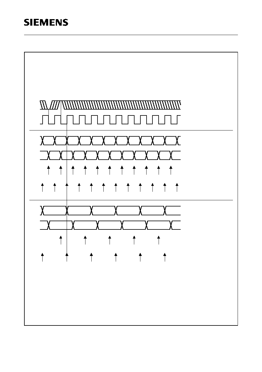
PEB 2055
PEF 2055
Application Hints
Semiconductor Group
94
Figure 24
PCM Interface Framing Offset for PMOD:PSM = 0
ITT08039
1st Bit
2nd Bit 3rd Bit
...
...
...
...
...
...
...
...
PFS
PDC
TxD#
TxD#
RxD#
RxD#
PMOD PSM = 0
0,
=
PCR
PMOD
URE = 1
Conditions:
0
=
URE
PCR = 0,
0,
=
PCR
DRE = 0
1
=
DRE
PCR = 0,
...
...
1,
=
PCR
DRE = 1
0
=
DRE
PCR = 1,
1,
=
PCR
URE = 0
1
=
URE
PCR = 1,
RxD#
RxD#
TxD#
TxD#
:
:
:
PMOD
:
PMOD
:
PMOD
PMOD :
PMOD :
PMOD :
:
PMOD
:
PCSR
PCSR :
PCSR :
PCSR :
:
PCSR
:
PCSR
:
PCSR
PCSR :
1st Bit
2nd Bit 3rd Bit
3rd Bit
3rd Bit
2nd Bit
2nd Bit
1st Bit
1st Bit
3rd Bit
2nd Bit
2nd Bit
3rd Bit
3rd Bit
2nd Bit
2nd Bit
3rd Bit
1st Bit
1st Bit
1st Bit
1st Bit
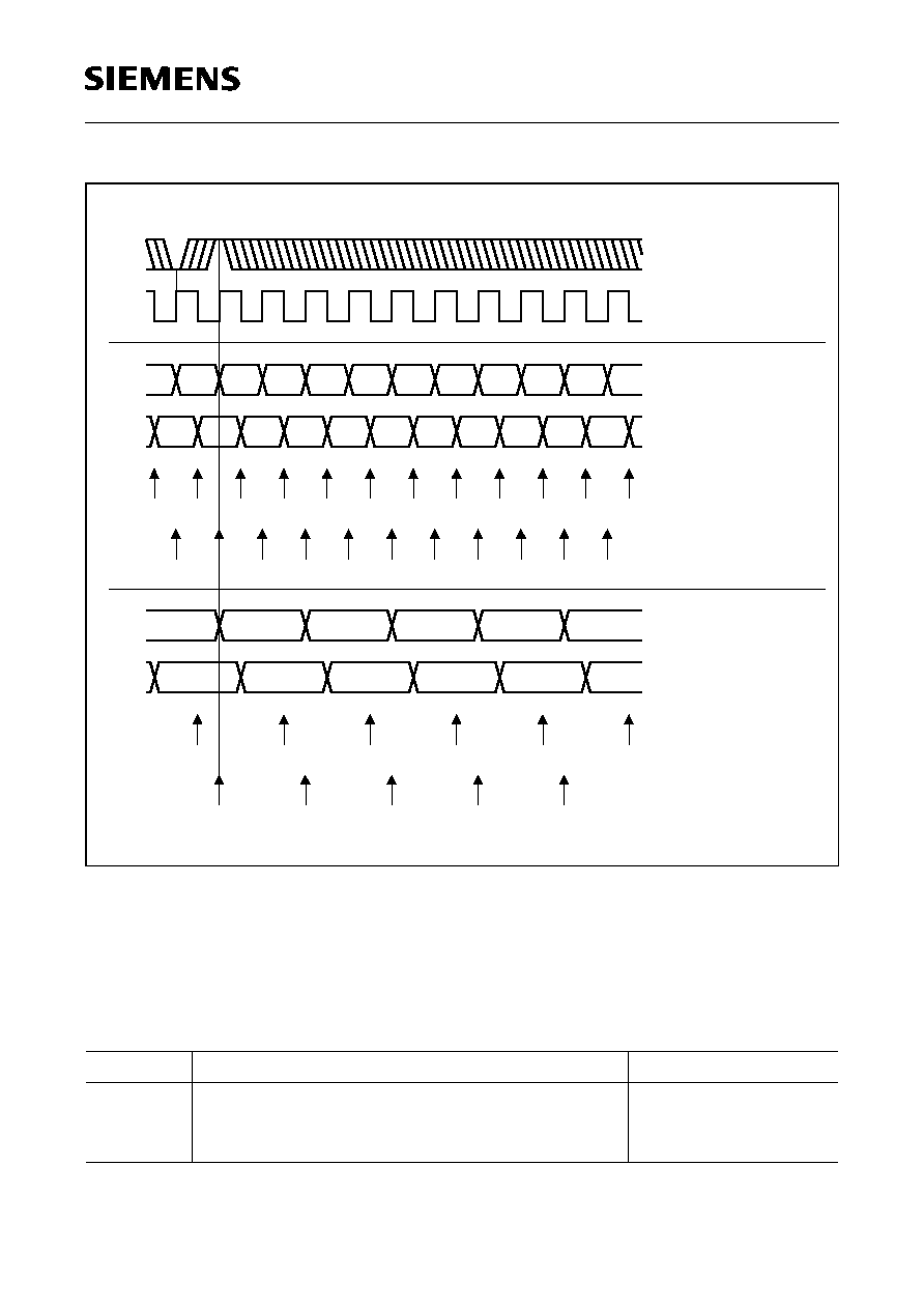
PEB 2055
PEF 2055
Application Hints
Semiconductor Group
95
Figure 25
PCM Interface Framing for PMOD:PSM = 1
The formulas given in table 11 and table 12 apply for calculating the values to be
programmed to the offset registers (OFD, OFU) given the desired bit number (BND,
BNU) to be marked. BPF denotes the actual number of bits constituting a frame.
Table 11
PCM Mode Offset Downstream, POFD, PCSR
Remarks
0
1
2
OFD9 ... 2 = (BND ≠ 17 + BPF)
mod BPF
OFD9 ... 1 = (BND ≠ 33 + BPF)
mod BPF
OFD9 ... 0 = (BND ≠ 65 + BPF)
mod BPF
PCSR:OFD1 ... 0 = 0
PCSR:OFD0 = 0
≠
ITT08040
...
...
...
...
...
...
...
...
PFS
PDC
TxD#
TxD#
RxD#
RxD#
Conditions:
...
...
RxD#
RxD#
TxD#
TxD#
...
:
PCSR
PCSR :
PCSR :
PCSR :
:
PCSR
:
PCSR
:
PCSR
PCSR :
PMOD :
:
PMOD
:
PMOD
:
PMOD
PMOD :
PMOD :
PMOD :
:
:
1,
=
PCR
URE = 1
0
=
URE
PCR = 1,
1,
=
PCR
DRE = 0
1
=
DRE
PCR = 1,
0,
=
PCR
DRE = 1
0
=
DRE
PCR = 0,
0,
=
PCR
URE = 0
1
=
URE
PMOD PCR = 0,
1
=
PSM
PMOD
3rd Bit
2nd Bit
1st Bit
1st Bit
1st Bit
1st Bit
2nd Bit 3rd Bit
3rd Bit
3rd Bit
2nd Bit
2nd Bit
1st Bit
2nd Bit
3rd Bit
3rd Bit
2nd Bit
1st Bit
1st Bit
2nd Bit
3rd Bit
3rd Bit
2nd Bit
1st Bit

PEB 2055
PEF 2055
Application Hints
Semiconductor Group
96
Examples
1) In PCM mode 0, with a frame consisting of 32 time slots, the following timing
relationship between the framing signal and the data signals is required:
Figure 26
Timing PCM Frame Offset for Example 1
Table 12
PCM Mode
Offset Upstream, POFU, PCSR
Remarks
0
1
2
OFU9 ... 2 = (BNU + 23)
mod BPF
OFU9 ... 1 = (BNU + 47)
mod BPF
OFU9 ... 0 = (BNU + 95)
mod BPF
PCSR:OFU1 ... 0 = 0
PCSR:OFU0 = 0
≠
ITT08041
Start of Internal Frame
0
1
PFS
PDC
TxD#
BNU
PMOD PSM = 0
1
=
URE
PCSR
Offset
and Bit
Time-Slot
Required
2
Bit 6
BND
RxD#
DRE = 0
1
Bit 7
3
Bit 5
4
Bit 4
5
Bit 3
6
Bit 2
7
Bit 1
8
Bit 0
9
10
Time-Slot 0
256
:
:
:
PCSR

PEB 2055
PEF 2055
Application Hints
Semiconductor Group
97
The PCM interface shall be clocked with a PDC having the same frequency as the data
rate i.e. 2.048 MHz. Since the rising edge of PFS occurs at the same time as the rising
edge of PDC, it is recommended to select the falling PDC edge for sampling the PFS
signal (PMOD:PSM0 = 0). In this case the 1st bit of internal framing structure (according
to figure 26) will represent time slot 0, bit 6 (2nd bit) of the external frame (according to
figure 24). The values to be programmed to the POFD, POFD and PCSR can now be
determined as follows:
With BND = BNU = 2 and BPF = 256:
POFD = OFD9 ... 2 = (BND ≠ 17 + BPF)
mod BPF
= (2 ≠ 17 + 256)
mod 256
= 241
D
= F1
H
POFU = OFU9 ... 2 = (BNU + 23)
mod BPF
= (2 + 23)
mod 256
= 25
D
= 19
H
With URE = 1 and DRE = 0:
PCSR = 01
H
2) In PCM mode 1, with a frame consisting of 48 time slots, the following timing
relationship between the framing signal and the data signals is required:
Figure 27
Timing for PCM Frame Offset of Example 2
ITT08042
Start of Internal Frame
0
1
PFS
PDC
TxD#
BNU
Bit 2
Bit 1
Bit 0
Bit 3
Bit 7
Bit 6
Bit 5
384
383
382
1
2
3
381
Time-Slot 47
Time-Slot 0
Required
Time-Slot/Bit
Offset in
Upstream
Direction
Downstream
Offset in
Time-Slot/Bit
Required
5
4
1
2
3
Bit 3
Bit 4
Bit 5
Bit 6
Bit 7
Direction
Time-Slot 0
Bit 2
6
BND
RxD#
PCSR :
:
:
1
=
DRE
PCSR URE = 1
1
=
PSM
PMOD

PEB 2055
PEF 2055
Application Hints
Semiconductor Group
98
The PCM interface shall be clocked with a PDC having twice the frequency of the data
rate i.e. 6144 kHz. Since the rising edge of PFS occurs a little bit before the rising edge
of PDC i.e. the set-up and hold times with respect to the rising PDC are met, it is possible
to select the rising PDC edge for sampling the PFS signal (PMOD:PSM = 1). In this case
the 1st bit of the internal framing structure (according to figure 27) will represent time
slot 47, bit 1 (383rd bit) in upstream and time slot 0, bit 5 (3rd bit) in downstream direction
of the external frame (according to figure 25). The values to be programmed to the
POFD, POFD and PCSR can now be determined as follows:
With BND = 3, BNU = 383 and BPF = 384:
OFD9 ... 1 = (BND ≠ 33 + BPF)
mod BPF
= (3 ≠ 33 + 384)
mod 384
= 354
D
= 1 0110 0010
B
OFU9 ... 1 = (BNU + 47)
mod BPF
= (383 + 47)
mod 384
= 46
D
= 0001 0111 0
B
POFD = 1011 0001
B
= B1
H
,
POFU = 1000 1111
B
= 17
H
With URE = 1 and DRE = 1:
PCSR = 0001 0001
B
= 11
H
,
PCM Receive Line Selection PMOD:AIS1 ... AIS0
The PCM transmit line of a given logical port (as it is used for programming the switching
function) is always assigned to a dedicated physical transmit pin, e.g. in PCM mode 1,
pin TxD2 carries the PCM data of logical port 1.
In receive direction however, an assignment between logical and physical ports can be
made in PCM modes 1 and 2. This selection is programmed via the Alternative Input
Selection bits 1 and 0 (AIS1, AIS0) in the PMOD register.
In PCM mode 0, AIS1 and AIS0 should both be set to 0.
In PCM mode 1, AIS0 selects between receive lines RxD0 and RxD1 for logical port 0
and AIS1 between the receive lines RxD2 and RxD3 for logical port 1.
In PCM mode 2, AIS1 selects between the receive lines RxD2 and RxD3, the setting of
AIS0 is don't care.
The state of the AIS# bits is furthermore put out via the TSC# pins and can thus be used
to control external circuits (drivers, relays ... ).

PEB 2055
PEF 2055
Application Hints
Semiconductor Group
99
Table 13 shows the function taken on by each of the PCM interface pins, depending on
the PCM mode and the values programmed to AIS1 and AIS0.
Figure 28 shows the correlation between physical and logical PCM ports for PCM
modes 0, 1, 2, 3:
Figure 28
Correlation between Physical and Logical PCM Ports
Table 13
PCM
Mode
Port 0
Port 1
Port 2
Port 3
RxD0
TxD0
TSC0
RxD1
TxD1
TSC1
RxD2
TxD2
TSC2
RxD3
TxD3
TSC3
0
IN0
OUT0
TSC0
IN1
OUT1
TSC1
IN2
OUT2
TSC2
IN3
OUT3
TSC3
1
IN0 for
AIS0=1
OUT0
TSC0
IN0 for
AIS0=0
high Z AIS0
IN1 for
AIS1=1
OUT1
TSC1
IN1 for
AIS1=0
high Z AIS1
2
≠
OUT
TSC
≠
high Z AIS0
IN for
AIS1=1
undef. undef. IN for
AIS1=0
high Z AIS1
ITS09545
Logical Ports:
OUT1
AIS1
PMOD:
0
1
IN1
EPIC
PCM Mode 0
Logical Ports:
OUT0
Physical
Pins:
IN0
IN1
OUT1
IN2
OUT2
IN3
OUT3
Pins:
Physical
Logical Ports:
Physical
Pins:
TSC0
TxD0
TSC0
RxD0
TSC1
TSC1
TxD1
RxD1
TxD2
TSC2
TSC2
RxD2
TxD3
TSC3
TSC3
RxD3
RxD2
TSC3
RxD3
TxD2
TSC1
TSC2
TSC0
TSC0
TxD0
RxD1
TSC1
RxD0
IN0
1
0
PMOD:
AIS0
OUT0
PMOD:
AIS0
TSC1
RxD3
TSC3
RxD2
IN
1
0
PMOD:
AIS1
TSC
TSC0
OUT
TxD0
EPIC
EPIC
PCM Mode 1
PCM Mode 2
R
R
R

PEB 2055
PEF 2055
Application Hints
Semiconductor Group
100
PCM Input Comparison PMOD:AIC1 ... AIC0
If the PCM input comparison is enabled, the EPIC checks the contents of two PCM
receive lines (physical ports) against each other for mismatches. (Also refer to
chapter 5.8.2).
The comparison function is operational in all PCM modes, a redundant PCM line which
can be switched over to by means of the PMOD:AIS bits is of course only available in
PCM modes 1and 2.
AIC0 set to logical 1 enables the comparison function between RxD0 and RxD1.
AIC1 set to logical 1 enables the comparison function between RxD2 and RxD3.
AIC1, AIC0 set to logical 0 disables the respective comparison function.
PCM Standby Mode OMDR:PSB
In standby mode (OMDR:PSB = 0), the PCM interface output pins TxD0 ... 3 are set to
high impedance and those (TSC#) pins which are actually used as tristate control signals
are set to logical 1 (inactive).
Note that the internal operation of the EPIC is not affected in standby mode, i.e. the
received PCM data is still written into the downstream data memory and may still be
processed by the EPIC (switched to the CFI or to the
Ķ
P, compared with other input line,
etc.)
In operational mode (OMDR:PSB = 1), the PCM output pins transmit the contents of the
upstream data memory data field or may be set to high impedance via the data memory
tristate field (refer to chapter 5.3.3.2).

PEB 2055
PEF 2055
Application Hints
Semiconductor Group
101
PCM Test Loop OMDR:PTL
The PCM test loop function can be used for diagnostic purposes if desired. If however a
"simple" CFI to CFI connection (CFI
PCM
CFI loop) shall be established, it is
recommended to program the PCM loop in the control memory (refer to
chapter 5.4.3.1).
If OMDR:PTL is set to logical 1, the test loop is enabled i.e. the physical transmit pins
TxD# are internally connected to the corresponding physical receive pins RxD#, such
that data transmitted over TxD# are internally looped back to RxD# and data externally
received over RxD# are ignored. The TxD# pins still output the contents of the upstream
data memory according to the setting of the tristate field.
Note: This loop back function can only work if the upstream and downstream bit shifts
match and if the port assignment (PMOD:AIS1 ... 0) is such that a logical
transmitter is looped back to a logical receiver (e.g. the PTL loop cannot work in
PCM mode 2!).
For normal operation OMDR:PTL should be set to logical 0 (test loop disabled).
Figure 29 illustrates the effect of the PTL bit:
Figure 29
Effect of the OMDR:PTL Bit
ITS09546
From Upstream
TxD#
OMDR PTL
EPIC
PCM Interface
1
0
Data Memory
To Downstream
Data Memory
RxD#
:
R

PEB 2055
PEF 2055
Application Hints
Semiconductor Group
102
5.2.2
Configurable Interface Configuration
5.2.2.1 CFI Interface Signals
The configurable interface signals are summarized in the table below:
1) Only EPIC-1
5.2.2.2 CFI Registers
The characteristics at the configurable interface (timing, modes of operation, etc. ... ) are
programmed in the 6 CFI interface registers and the Operation Mode Register OMDR.
The function of each bit is described in chapter 5.2.2.3. For addresses refer to
chapter 4.1.
CFI Mode Register 1
read/write
reset value:
00
H
Table 14
Pin No.
Symbol
I: Input
O: Output
Function
40
41
42
1)
43
1)
DD0/SIP0
DD1/SIP1
DD2/SIP2
DD3/SIP3
O/IO
O/IO
O/IO
O/IO
Data downstream outputs in CFI modes 0, 1 and 2
(PCM and IOM applications).
Bidirectional serial interface ports in CFI mode 3
(SLD application).
Tristate or open drain output drivers selectable
(OMDR:COS).
38
37
36
1)
35
1)
DU0/SIP4
DU1/SIP5
DU2/SIP6
DU3/SIP7
I/IO
I/IO
I/IO
I/IO
Data upstream inputs in CFI modes 0, 1 and 2
(PCM and IOM applications).
Bidirectional serial interface ports in CFI mode 3
(SLD application).
Tristate or open drain output drivers for SIP lines
selectable (OMDR:COS).
34
FSC
I or O
Frame synchronization input (CMD1:CSS = 1) or
output (CMD1:CSS = 0).
33
DCL
I or O
Data clock input (CMD1:CSS = 1) or output
(CMD1:CSS = 0).
bit 7
bit 0
CMD1
CCS
CSM
CSP1
CSP0
CMD1
CMD0
CIS1
CIS0

PEB 2055
PEF 2055
Application Hints
Semiconductor Group
103
CFI Mode Register 2
read/write
reset value:
00
H
CFI Bit Number Register
read/write
reset value:
FF
H
CFI Time Slot Adjustment Register
read/write
reset value:
00
H
CFI Bit Shift Register
read/write
reset value:
00
H
CFI Bit Subchannel Register
read/write
reset value:
00
H
Operation Mode Register
read/write
reset value:
00
H
bit 7
bit 0
CMD2
FC2
FC1
FC0
COC
CXF
CRR
CBN9
CBN8
bit 7
bit 0
CBNR
CBN7
CBN6
CBN5
CBN4
CBN3
CBN2
CBN1
CBN0
bit 7
bit 0
CTAR
0
TSN6
TSN5
TSN4
TSN3
TSN2
TSN1
TSN0
bit 7
bit 0
CBSR
0
CDS2
CDS1
CDS0
CUS3
CUS2
CUS1
CUS0
bit 7
bit 0
CSCR
SC31
SC30
SC21
SC20
SC11
SC10
SC01
SC00
bit 7
bit 0
OMDR
OMS1
OMS0
PSB
PTL
COS
MFPS
CSB
RBS

PEB 2055
PEF 2055
Application Hints
Semiconductor Group
104
5.2.2.3 CFI Characteristics
In the following the configurable interface characteristics that can be programmed in the
CFI registers are explained in more detail.
CFI Mode CMD1:CMD1, CMD0
The CFI mode primarily defines the actual number of CFI ports that can be used for
switching purposes (logical ports). 1, 2 or 4 duplex or 8 bidirectional logical CFI ports can
be selected. Since the channel capacity of the EPIC is constant (128 channels/direction),
the CFI mode also influences the maximum possible data rate.
In each CFI mode a reference clock (RCL) of a specific frequency is required. This clock
may be derived from the PCM clock signal PDC (CMD1:CSS = 0) or from the DCL signal
(CMD1:CSS = 1). Also refer to figure 30 and figure 31.
Table 15 states the specific characteristics of each CFI mode.
(DR = CFI data rate, N = number of 8 bit time slots in PCM frame, du = duplex port,
bi = bidirectional port).
Note: The label is used to specify a CFI port when programming a switching function. It
should not be confused with the physical port number which refers to actual
hardware pins. The relationship between logical and physical port numbers is
given in table 19 and is illustrated in figure 46.
Table 15
CMD1 CMD0 CFI
Mode
Number
(Label) of
Logical
Ports
CFI Data
Rate
[kbit/s]
Min. Required
CFI DR
[kbit/s]
relative to
PCM Data
Rate
Necessary
Reference
Clock
(RCL)
DCL Output
Frequencies
CMD1:
CSS = 0
min.
max.
1
0
0
1
1
0
1
0
3
0
1
2
8 bi (0 ... 7)
4 du (0 ... 3)
2 du (0 ... 1)
1 du
128
128
128
128
1024
2048
4096
8192
16N/3
32N/3
64N/3
64N/3
4
◊
DR
2
◊
DR
DR
0.5
◊
DR
DR, 2
◊
DR
DR, 2
◊
DR
DR
DR

PEB 2055
PEF 2055
Application Hints
Semiconductor Group
105
Important Note
It should be noticed that there are some restrictions concerning the PCM to CFI data rate
ratio. If the CFI data rate is chosen higher than the PCM data rate, no restrictions apply.
If however the CFI data rate is lower than the PCM data rate, a minimum CFI date rate
relative to the PCM data rate must be maintained (refer also to examples below).
Another important restriction is, that the number of bits per CFI frame must always be
modulo 16.
Examples
If the PCM frame consists of 32 time slots (2.048 Mbit/s), the minimum possible CFI data
rate in CFI mode 0 is (32
◊
32)/3 = 341.3 kbit/s or if rounded to an integer number of time
slots 344 kbit/s. It is thus not possible to have an IOM-1 interface with 256 kbit/s together
with a 2.048 Mbit/s PCM interface in CFI mode 0. If instead the PCM frame consists of
24 time slots (1.536 Mbit/s), the IOM-1 data rate of 256 kbit/s is feasible since
(24
◊
32)/3 = 256 kbit/s.
CFI Clock and Framing Signal Source CMD1:CSS
The PCM interface is always clocked and synchronized by the PDC and PFS input
signals. The configurable interface however can be clocked and synchronized either by
signals internally derived from PDC and PFS or it can be clocked and synchronized by
the externally applied DCL and FSC input signals.
If PDC and PFS are selected as clock and framing signal source (CMD1:CSS = 0),
the CFI reference clock CRCL is obtained out of PDC after division by 1, 1.5 or 2
according to the prescaler selection (CMD:CSP1 ... 0). The CFI frame structure is
synchronized by the PFS input signal. The EPIC generates DCL and FSC as output
signals which may be specified by CMD2:COC (DCL clock rate) and CMD2:FC2 ... 0
(FSC pulse form). This mode should be selected whenever the required CFI data rate
can be obtained out of the PCM clock source using the internal prescalers. An overview
of the different possibilities to generate the PCM and CFI data and clock rates for
CMD1:CSS = 0 is given in figure 30.

PEB 2055
PEF 2055
Application Hints
Semiconductor Group
106
Figure 30
EPIC
ģ
Clock Sources for the CFI and PCM Interfaces if CMD1:CSS = 0
If DCL and FSC are selected as clock and framing signal source (CMD1:CSS = 1),
the CFI reference clock CRCL is obtained out of the DCL input signal after division by 1,
1.5 or 2 according to the prescaler selection (CMD1:CSP1 ... 0). The CFI frame
structure is synchronized by the FSC input signal. Note that although the frequency and
phase of DCL and FSC may be chosen almost independently with respect to the
frequency and phase of PDC and PFS, the CFI clock source must still be synchronous
to the PCM interface clock source i.e. the two clock sources must always be derived from
one master clock. This mode must be selected if it is impossible to derive the required
CFI data rate from the PCM clock source. An overview of the different possibilities to
generate the PCM and CFI data and clock rates for CMD1:CSS = 1 is given in figure 31.
ITS09547
3
0
1
2
CFI Mode
Internal Reference
Clock (RCL)
CFI Mode
2
1
0
3
CMD1 CSP1,
COC
CMD2
x2
*
Only CFI
*
Modes
FC Modes 0-7
CMD2 FC2
DCL
FSC
Bit Shift
CTAR
CBSR: CDS2...0
Bit Shift
POFU
POFD
PCSR
PMOD PCR
PCM Frame Sync.
PCM Data Rate
CFI Data Rate
CFI Frame Sync.
PDC
PFS
EPIC
2
:
:
:
:
0
...0
0 and 3
CRCL
M
U
X
X
U
M
X
X
U
U
M
M
P
C
M
C
F
I
M
U
X
4
2
1.5
2
2
R

PEB 2055
PEF 2055
Application Hints
Semiconductor Group
107
Figure 31
EPIC
ģ
Clock Sources for the CFI and PCM Interfaces if CMD1:CSS = 1
CFI Clock Source Prescaler CMD1:CSP1 ... 0
The CFI clock source PDC (CMD1:CSS = 0) or DCL (CMD1:CSS = 1) can be divided by
a factor of 1, 1.5 or 2 in order to obtain the CFI reference clock CRCL (see table 16).
Note that in CFI mode 2, the frequency of RCL is only half the CFI data rate.
Table 16
CSP1
CSP0
Prescaler Divisor
0
0
1
1
0
1
0
1
2
1.5
1
not allowed
ITS09548
Bit Shift
CTAR
CBSR: CDS2...0
EPIC
CFI Frame Sync.
CFI Data Rate
PCM Frame Sync.
PCM Data Rate
PFS
PDC
DCL
FSC
3
0
1
2
2
1
0
3
CFI Mode
CFI Mode
Internal Reference
Clock (RCL)
PCSR
POFD
POFU
Bit Shift
2
CRCL
0
: CSP1,
CMD
: PCR
PMOD
1.5
2
M
U
X
2
4
2
M
U
X
P
C
M
C
F
I
R

PEB 2055
PEF 2055
Application Hints
Semiconductor Group
108
Figure 32 shows the relationship between the DCL input and the generated RCL for the
different prescaler divisors in case CMD1:CSS = 1:
Figure 32
Clock Signal Timing for the Different Prescaler Divisors if CMD1:CSS = 1
CFI Clock Output Rate CMD2:COC
This feature applies only if the configurable interface is clocked and synchronized via the
PCM interface clock and framing signals (PDC, PFS), i.e. if CMD1:CSS = 0.
In this case the EPIC delivers an output clock signal at pin DCL with a frequency identical
to or double the selected CFI data rate:
For CMD2:COC = 0, the frequency of DCL is identical to the CFI data rate
(all CFI modes)
For CMD2:COC = 1, the frequency of DCL is twice the CFI data rate
(CFI modes 0 and 3 only!)
ITT08047
FSC
CMD1 : CSM = 1
FSC
DCL
Conditions:
RCL
CFI Modes 0, 1 and 3
RCL
RCL
RCL
RCL
RCL
0
=
CSM
:
CMD1
CFI Mode 2
Prescaler Divisor 1.5
CMD1
:
CSP1
...
0
=
01
00
=
0
...
CSP1
:
CMD1
Prescaler Divisor 2
10
=
0
CSP1
:
CMD1
Prescaler Divisor 1
...
CMD1
:
CSS
=
1
CFI Modes 0, 1 and 3
CFI Mode 2
CFI Modes 0, 1 and 3
CFI Mode 2

PEB 2055
PEF 2055
Application Hints
Semiconductor Group
109
Figure 33 shows the relationship between the PFS, PDC, RCL and DCL signals in the
different CFI modes.
Figure 33
Clock Signal Timing for the Different Prescaler Divisors if CMD1:CSS = 0
ITT08048
PFS
PFS
PDC
Conditions:
RCL
RCL
DCL
DCL
DCL
DCL
DCL
DCL
RCL
RCL
RCL
RCL
DCL
DCL
DCL
1
=
CSS
:
CMD1
Prescaler Divisor 2
CMD1
:
CSP1
...
0
=
00
01
=
0
...
CSP1
:
CMD1
Prescaler Divisor 1.5
10
=
0
...
CSP1
:
CMD1
Prescaler Divisor 1
CFI Mode 2
0,1 and 3
CFI Modes
CMD1 : CSM = 0
1
=
CSM
:
CMD1
/
/
PMOD : PSM = 1
0
=
PSM
:
PMOD
0,
CFI Mode
CFI Modes 1 and 2
1
=
COC
:
CMD2
CMD2 : COC = 0
CFI Mode 0,
3,
CFI Mode
1
=
COC
:
CMD2
CMD2 : COC = 0
CFI Mode 3,
3,
CFI Mode
0
=
COC
:
CMD2
CMD2 : COC = 1
CFI Mode 3,
0,
CFI Mode
0
=
COC
:
CMD2
CMD2 : COC = 1
1 and 2
CFI Modes
CFI Mode 0,
CFI Modes
1 and 3
0,
2
CFI Mode
CFI Mode 2
0,1 and 3
CFI Modes
0,
CFI Mode
CFI Modes 1 and 2
1
=
COC
:
CMD2
CMD2 : COC = 0
CFI Mode 0,
3,
CFI Mode
1
=
COC
:
CMD2
CMD2 : COC = 0
CFI Mode 3,

PEB 2055
PEF 2055
Application Hints
Semiconductor Group
110
CFI Framing Signal Output Control CMD2:FC2 ... 0
This feature applies only if the configurable interface is clocked and synchronized via the
PCM interface clock and framing signals (PDC, PFS), i.e. if CMD1:CSS = 0.
In this case the EPIC delivers an output framing signal at pin FSC with a programmable
pulse width and position.
Note that the up- and downstream CFI frame position relative to the FSC output is not
affected by the setting of the CTAR and CBSR:CDS2 ... 0 register bits.
Table 17 summarizes the 7 possible FSC Control (FC) modes:
Table 17
FC2
FC1
FC0
FC
Mode
Main Applications
Notes
0
0
0
0
1
1
1
1
0
0
1
1
0
0
1
1
0
1
0
1
0
1
0
1
0
1
2
3
4
5
6
7
IOM-1 multiplexed (burst) mode
General purpose
General purpose
General purpose
Special SLD application
reserved
IOM-2, IOM-1 or SLD modes
Software timed multiplexed
IOM-2 applications
SBC, IBC, IEC-T
2 ISAC-S per SLD port
Standard IOM-2 setting;
no Superframes
generated
Standard IOM-2 setting;
Superframes generated

PEB 2055
PEF 2055
Application Hints
Semiconductor Group
111
Figure 34 and figure 35 show the position of the FSC pulse relative to the CFI frame:
Figure 34
Position of the FSC Signal for FC Modes 0, 1, 2, 3 and 6
Figure 35
Position of the FSC Signal for FC Modes 4 and 6
ITT08049
Conditions:
RCL
DCL
DCL
FSC
CFI Mode 0;
CFI Modes 1, 2;
1
=
COC
:
CMD2
DCL
CFI Frame
Last Time-Slot of a Frame
Time-Slot 0
CMD2 : COC = 0
FSC
FSC
FSC
FSC
1
=
COC
:
CMD2
CMD2 : COC = 0
CFI Modes 3;
CFI Mode 0;
CFI Modes 3; COC = 0
CMD2 : FC2
= 011
... 0
(FC Mode 3)
(FC Mode 2)
0
...
010
=
FC2
:
CMD2
(FC Mode 0)
0
...
000
=
FC2
:
CMD2
(FC Mode 1)
0
...
001
=
FC2
:
CMD2
(FC Mode 6)
0
...
110
=
FC2
:
CMD2
ITT08050
0
1
2
3
4
5
FSC
CFI Frame
FSC
RCL
(FC mode 6)
110
=
...
FC2
CMD2 :
Conditions:
Time-Slot
0
0
:
CMD2 FC2 ... = 100 (FC mode 4)

PEB 2055
PEF 2055
Application Hints
Semiconductor Group
112
Application Examples of the Different FC Modes
FC Mode 0
FC mode 0 applies for IOM-1 multiplexed mode applications, i.e. for IOM-1 interfaces
with 2.048 Mbit/s data rate. Accommodated layer-1 devices: SBC (PEB 2080),
IBC (PEB 2095), IEC-T (PEB 20901/20902), ...
In IOM-1 mux. mode, the frame is synchronized with a negative pulse with a duration of
one DCL period which marks bit number 251. The bits are transmitted with the falling
clock edge and received with the rising clock edge.
Required register setting: CMD1 = 0XXX0000
B
, CMD2 = 1C
H
, CBNR = FF
H
,
CTAR = XX
H
, CBSR = X0
H
.
Figure 36 shows the relationship between FSC, DCL, DD# and DU#:
Figure 36
Multiplexed IOM
ģ
-1 Interface Signals
FC Mode 1
FC mode 1 is similar to FC mode 0. The FSC pulse is shifted by half a RCL period to the
right compared to FC mode 0. It can be used for general purposes.
FC Mode 2
FC mode 2 is similar to FC mode 3. The FSC pulse is shifted by half a RCL period to the
left compared to FC mode 3. It can be used for general purposes.
ITT08051
FSC
DCL
DD#
DU#
TS31, Bit 4
Bit 5
TS31,
Bit 4
TS31,
TS31, Bit 3
TS31, Bit 2
TS31, Bit 1
Bit 0
TS31,
Bit 7
TS0,
Bit 3
TS31,
Bit 2
TS31,
Bit 1
TS31,
Bit 0
TS31,
TS0, Bit 7
Bit 6
TS0,
Bit 5
TS0,
TS0, Bit 4
TS0, Bit 6
Bit 5
TS0,
TS0, Bit 4

PEB 2055
PEF 2055
Application Hints
Semiconductor Group
113
FC Mode 3
FC mode 3 can be used for IOM-2 applications, but it should be noted that some IOM-2
layer-1 transceivers will interpret an FSC pulse of only one DCL period as a superframe
marker (e.g. SBCX PEB 2081, IEC-Q PEB 2091, ... ), and it is not allowed to provide a
superframe marker in every frame. For these applications it is recommended to use
either FC mode 6 or FC mode 7.
FC Mode 4
FC mode 4 applies for special SLD applications like 2 ISAC-S devices connected to one
SIP line. Usually each SIP line carries the two 64 kbit/s B channels followed by a feature
control and a signaling channel. The feature control and signaling channels however are
not required for all applications. This is, for example, the case if a digital subscriber circuit
(S- or U- layer-1 transceiver) is connected via an ISDN Communication Controller
(ICC PEB 2070) to the EPIC. The task of the ICC is to handle the D-channel and to
switch the B1 and B2 channels from the SLD to the IOM-1 interface. The capacity of such
an SLD line card can be doubled if the unused time slots for the feature control and
signaling channels are also used as 64 kbit/s B channels. This is possible if the
additionally connected ICC (or ISAC-S) is synchronized with an FSC that is delayed by
2 time slots i.e. the rising FSC edge is at the beginning of time slot 2 instead of 0. The
CFI time slots 2, 3, 6 and 7 can then be programmed as normal B channels within the
EPIC instead of being programmed as feature control and signaling channels.
FC Mode 6
This is the most often used type of FSC signal, because it covers the standard IOM-1,
IOM-2 and SLD applications. The rising edge of FSC marks time slot 0, bit 7 of the CFI
frame.
The pulse width is 32 bits or 4 time slots, i.e. the FSC is symmetrical (duty cycle 1:1) if
the CFI frame consists of 8 time slots (SLD), and the FSC is high during the first IOM-2
channel if the CFI frame consists of 32 time slots (IOM-2).

PEB 2055
PEF 2055
Application Hints
Semiconductor Group
114
Required register setting for IOM-2:
CMD1 = 0XXX0000
B
, CMD2 = D0
H
, CBNR = FF
H
, CTAR = XX
H
, CBSR = X0
H
.
Figure 37 shows the relationship between FSC, DCL, DD# and DU#:
Figure 37
IOM
ģ
-2 Interface Signals
Required register setting for SLD:
CMD1 = 0XXX1100
B
, CMD2 = D0
H
, CBNR = 1F
H
, CTAR = XX
H
, CBSR = X0
H
.
Figure 38 shows the relationship between FSC, DCL and SIP#:
Figure 38
SLD Interface Signals
ITT08052
FSC
DCL
DD#
DU#
TS31, Bit 1
Bit 0
TS31,
TS0, Bit 7
TS0, Bit 7
TS0, Bit 6
Bit 5
TS0,
Bit 4
TS0,
Bit 3
TS0,
Bit 2
TS0,
Bit 1
TS0,
Bit 0
TS0,
Bit 0
TS31,
TS0, Bit 6
Bit 5
TS0,
Bit 4
TS0,
Bit 3
TS0,
Bit 2
TS0,
Bit 1
TS0,
Bit 0
TS0,
ITT08053
FSC
DCL
SIP#
(OUT)
TS0, Bit 7
Bit 4
TS7,
RCL
(IN)
SIP#
TS0, Bit 6
TS0, Bit 5
TS0, Bit 4
TS0, Bit 3
TS7, Bit 3
Bit 2
TS7,
TS7, Bit 1
Bit 0
TS7,

PEB 2055
PEF 2055
Application Hints
Semiconductor Group
115
FC Mode 7
FC mode 7 is intended for IOM-2 line cards to synchronize the multiframe structure
among several S- or U
k
-interface transceivers. The layer-1 multiframe is reset by an FSC
pulse having a width of at most, one DCL period. Between the multiframe reset pulses,
FSC pulses with a width of at least two DCL periods must be applied. Devices which
support this option are for example the OCTAT-P (PEB 2096-H), QUAT-S
(PEB 2084-H), SBCX (PEB 2081), and the IEC-Q (PEB 2091).
FC mode 7 is a combination of FC modes 3 and 6. The timer register TIMR must be
loaded with the required multiframe period (e.g. 5 ms for the S-interface or 12 ms for the
U
k
-interface). When the timer is started with CMDR:ST, a cyclic multiplexing process is
started: whenever the timer expires, the frame signal has the pulse shape of FC mode 3
during one frame. For all the other frames the FSC signal has the pulse form of FC
mode 6.
After setting the CMDR:ST bit, the inverted value of TVAL is loaded to the timer and the
timer is incremented as soon as time slot 3 is passed (i.e. the FSC high phase is passed
which lasts for 4 TSs in FC mode 6) and then every 250
Ķ
s.
When the timer expires (timer value = 0), an interrupt is generated immediately and the
next FSC pulse has the shape of FC mode 3.
Figure 39 illustrates this behavior for a timer value of TVAL6 ... 0 = 0000001.
Figure 39
FSC Signal in FC Mode 7
Note: If the timer is stopped, the generated pulse form is the one of FC mode 6.
Timer value examples:
Required timer value for 5 ms period: TIMR:TVAL6 ... 0 = 010011
B
, e.g. TIMR = 13
H
Required timer value for 12 ms period: TIMR:TVAL6 ... 0 = 101111
B
, e.g TIMR = 2F
H
ITT08054
n
n + 1
2
+
n
n + 3
n + 4
n + 5
n + 6
n + 7
n + 8
FC Mode 7
FSC
CFI Frame
Timer Loaded
CMFR: ST = 1
Timer
Incremented
Expired
Timer
Incremented
Timer
Timer
Expired

PEB 2055
PEF 2055
Application Hints
Semiconductor Group
116
CFI Bit Number CMD2, CBNR:CBN9 ... CBN0
The CFI data rate is determined by the reference clock RCL and the CFI mode selected
by CMD1:CMD1 ... 0. The number of bits which constitute a CFI frame can be derived
from this data rate by division of 8000 (8 kHz frame structure). If the CFI interface is for
example operated at 2.048 Mbit/s, the frame would consists of 256 bits or 32 time slots.
This number of bits must be programmed to CMD2,CBNR:CBN9 ... 0 as indicated
below. Note that the formula is valid for all CFI modes:
CBN9 ... 0 = number of bits ≠ 1
Examples
A CFI frame consisting of 64 time slots would require a setting of
CBN9 ... 0 = 64
◊
8 ≠ 1 = 511D = 01 1111 1111
B
A CFI frame consisting of 48 time slots would require a setting of
CBN9 ... 0 = 48
◊
8 ≠ 1 = 383D = 01 0111 1111
B
CFI Synchronization Mode CMD1:CSM
The CFI interface can either be synchronized via the PFS pin (CMD1:CSS = 0), or via
the FSC pin (CMD1:CSS = 1). A transition from low to high of either PFS or FSC
synchronizes the CFI frame. The PFS (FSC) signal is internally sampled with the PDC
(DCL) clock:
If CSM is set to logical 0, the PFS/FSC signal is sampled with the falling clock edge of
PDC/DCL, if set to logical 1, the PFS/FSC signal is sampled with the rising clock edge
of PDC/DCL.
If CMD1:CSS is set to logical 0 (CFI clocks are internally derived from the PCM clocks),
then CMD1:CSM should be equal to PMOD:PSM.
If CMD1:CSS is set to logical 1 (CFI clock signals are inputs), then CMD1:CSM should
be selected such that stable low and high phases of the FSC signal can be detected,
meeting the set-up (
T
FS
) and hold (
T
FH
) times with respect to the programmed DCL clock
edge.
The high phase of the PFS/FSC pulse may be of arbitrary length, however it must be
assured that it is sampled low at least once before the next framing pulse.
The relationship between the framing and clock signals (PFS, FSC, PDC, DCL and RCL)
for the different modes of operation is illustrated in figures 32 and 33.
Note: In case DCL and FSC are selected as inputs (CMD1:CSS = 1), FSC must always
be synchronized with the positive edge of DCL (CMD1:CSM = 1). Otherwise, an
IOM-2 compatible timing cannot be installed by means of a bit shift (When the
negative edge is used for synchronization the internal frame start is delayed by
one DCL clock. In double rate mode a bit shift of half a bit cannot be adjusted).
Anyway, if the rising edges of DCL and FSC do not meet the frame setup time
T
FS
,

PEB 2055
PEF 2055
Application Hints
Semiconductor Group
117
additional hardware must delay the frame signal to enable a synchronization with
the positive edge of DCL. Figure 40 gives a suggestion of how to adapt the
external timing.
Figure 40
Circuit for Delaying the Framing Signal at the CFI Interface
ITS08055
CLK
DOUT
DIN
SYNC
1st Bit
2nd Bit
3rd Bit
4th Bit
5th Bit
5th Bit
4th Bit
3rd Bit
2nd Bit
1st Bit
FSC
Rising FSC edge marks 2nd Bit of frame
PR
J
CLR
K
Q
Q
Q
Q
K
CLR
J
PR
FSC
DCL
(DU#)
(DD#)
SYNC
CLK
DIN
DOUT
+5 V
J-K Flip-Flop e.g. 74HC112
EPIC
+5 V
R

PEB 2055
PEF 2055
Application Hints
Semiconductor Group
118
CFI Bit Timing and Bit Shift CMD2, CTAR, CBSR
The position of the CFI frame can be shifted relative to the CFI frame synchronization
pulse using the CFI Time slot Adjustment Register CTAR and the CFI Bit Shift Register
CBSR. This shifting can be performed simultaneously for up- and downstream directions
with a one bit resolution by up to a whole frame. The upstream frame can additionally be
shifted relative to the downstream frame by up to 15 bits. Furthermore, the polarity of the
clock edge (CRCL) used for transmitting and sampling the data can be programmed in
the CMD2 register.
Since the frame synchronization source of the configurable interface is either PFS (for
CMD1:CSS = 0) or FSC (for CMD1:CSS = 1), the bit shift also refers to either the PFS
or the FSC framing signal.
Note: If PFS/PDC is selected as CFI sync/clock source, the time slot and bit shift
values programmed to CTAR and CBSR:CDS2 ... 0 affect both the CFI data lines
and the CFI output framing signal FSC. The CFI frame together with the FSC
signal can thus be shifted with respect to the PCM frame (PFS). The position of
the CFI frame relative to the FSC output signal is not affected by these settings
but is instead determined by the FSC framing control mode programmed to
CMD2:FC2 ... 0. The upstream CFI frame can, however, still be shifted relative to
the downstream CFI frame with the CBSR:CUS3 ... 0 bits.
If FSC/DCL is selected as CFI sync/clock source, the time slot and bit shift functions
affect the CFI frame with respect to the FSC framing input signal. In this case, the CFI
frame start can be selected completely independently from the PCM frame start, it must
only be assured that a phase relationship once established between the CFI and PCM
frames is maintained all the time.

PEB 2055
PEF 2055
Application Hints
Semiconductor Group
119
CFI Time Slot Adjustment and Bit Shift
If CBSR = 20
H
, the CFI framing signal (PFS if CMD1:CSS = 0 or FSC if CMD1:CSS = 1)
marks bit 7 of the CFI time slot called TSN according to the following formula:
CTAR:TSN6 ... 0 = TSN + 2
e.g. CTAR must be set to 02
H
if the framing signal should mark time slot 0, bit 7 (TS
= 0). See examples.
Note that the value of TSN may not exceed the actual number of time slots per CFI
frame:
TSN = [ ≠ 2; I ≠ 3], I = total number of time slots per CFI frame
From the zero offset bit position (CBSR = 20
H
) the CFI frame (downstream and
upstream) can be shifted by up to 5 bits to the left (within the time slot
number TSN programmed in CTAR) and by up to 2 bits to the right (within the previous
time slot N ≠ 1) by programming the CBSR:CDS2 ... 0 bits:
The bit shift programmed to CBSR:CDS2 ... 0 affects both the upstream and
downstream frame position in the same way.
If CBSR:CUS3 ... 0 = 0000, the upstream frame is aligned to the downstream frame.
With CBSR:CUS3 ... 0 = 0001 to 1111, the upstream CFI frame can be shifted relative
to the downstream frame by up to 15 bits to the left as indicated in figure 41.
Table 18
CBSR:CDS2 ... 0
Time Slot #
Marked Bit #
Bit Shift
000
001
010
011
100
101
110
111
TSN ≠ 1
TSN ≠ 1
TSN
TSN
TSN
TSN
TSN
TSN
1
0
7
6
5
4
3
2
2 bits to the right
1 bit to the right
no bit shift
1 bit to the left
2 bits to the left
3 bits to the left
4 bits to the left
5 bits to the left

PEB 2055
PEF 2055
Application Hints
Semiconductor Group
120
Figure 41
CFI Upstream Bit Shifting
ITT08056
DD#
Conditions:
DU#
DU#
DU#
DU#
DU#
DU#
DU#
DU#
DU#
DU#
DU#
DU#
DU#
DU#
DU#
DU#
CBSR:
CUS3...0
0000
0001
0010
0011
0100
0101
0110
0111
1000
1001
1010
1011
1100
1101
1110
1111
Bit 7
TS0,
TS1,
7
Bit
TS1, Bit 7
TS0, Bit 7
Bit 6
TS0,
TS0, Bit 5
Bit 4
TS0,
TS0, Bit 3
Bit 2
TS0,
Bit 1
TS0,
Bit 0
TS0,
Bit 6
TS0,
TS0, Bit 5 TS0, Bit 4 TS0, Bit 3 TS0, Bit 2 TS0, Bit 1 TS0, Bit 0
TS0, Bit 6
TS0, Bit 7
TS0, Bit 5 TS0, Bit 4 TS0, Bit 3 TS0, Bit 2 TS0, Bit 1 TS0, Bit 0
TS0, Bit 6
TS0, Bit 7
TS0, Bit 5 TS0, Bit 4 TS0, Bit 3 TS0, Bit 2 TS0, Bit 1 TS0, Bit 0
TS0, Bit 6
TS0, Bit 7
TS0, Bit 5 TS0, Bit 4 TS0, Bit 3 TS0, Bit 2 TS0, Bit 1 TS0, Bit 0
TS0, Bit 6
TS0, Bit 5
TS0, Bit 4
TS0, Bit 3
TS0, Bit 2
TS0, Bit 1
TS0, Bit 0
TS0, Bit 7
TS0, Bit 5 TS0, Bit 4 TS0, Bit 3 TS0, Bit 2 TS0, Bit 1 TS0, Bit 0
TS0, Bit 6
TS0, Bit 7
TS0, Bit 4 TS0, Bit 3 TS0, Bit 2 TS0, Bit 1 TS0, Bit 0
TS0, Bit 5
TS0, Bit 6
TS0, Bit 3 TS0, Bit 2 TS0, Bit 1 TS0, Bit 0
TS0, Bit 4
TS0, Bit 5
TS0, Bit 2 TS0, Bit 1 TS0, Bit 0
TS0, Bit 3
TS0, Bit 4
TS0, Bit 1 TS0, Bit 0
TS0, Bit 2
TS0, Bit 3
TS0, Bit 0
TS0, Bit 1
TS0, Bit 2
TS0, Bit 1
TS0, Bit 0
TS0, Bit 0
Bit 6
TS1,
TS1, Bit 7
TS1, Bit 6
TS1, Bit 5
TS1, Bit 4
TS1, Bit 3
TS1, Bit 2
TS1, Bit 1
TS1, Bit 7
TS1, Bit 5
TS1, Bit 6
TS1, Bit 7
TS1, Bit 4
TS1, Bit 5
TS1, Bit 6
TS1, Bit 3
TS1, Bit 2
TS1, Bit 4
TS1, Bit 5
TS1, Bit 6
TS1, Bit 7
TS1, Bit 1
TS1, Bit 3
TS1, Bit 4
TS1, Bit 5
TS1, Bit 6
TS1, Bit 7
TS1, Bit 0
Bit 2
TS1,
TS1, Bit 3
TS1, Bit 4
TS1, Bit 5
TS1, Bit 6
TS1, Bit 7
TS1, Bit 0
TS1, Bit 1
TS1, Bit 2
TS1, Bit 3
TS1, Bit 0
TS1, Bit 1
TS1, Bit 0
TS1, Bit 1
TS1, Bit 0
TS1, Bit 1
TS1, Bit 0
TS1, Bit 1
TS1, Bit 0
TS1, Bit 1
TS1, Bit 0
TS1, Bit 4
TS1, Bit 5
TS1, Bit 6
TS1, Bit 7
TS1, Bit 2
TS1, Bit 3
TS1, Bit 4
TS1, Bit 5
TS1, Bit 6
TS1, Bit 7
TS1, Bit 2
TS1, Bit 3
TS1, Bit 4
TS1, Bit 5
TS1, Bit 6
TS1, Bit 7
TS1, Bit 2
TS1, Bit 3
TS1, Bit 4
TS1, Bit 5
TS1, Bit 6
TS1, Bit 7
TS1, Bit 2
TS1, Bit 3
TS1, Bit 4
TS1, Bit 5
TS1, Bit 6
TS1, Bit 5
TS1, Bit 7
TS1, Bit 2
TS1, Bit 3
TS1, Bit 4
TS1, Bit 6
TS1, Bit 1
TS1, Bit 2
TS1, Bit 3
TS1, Bit 4
TS1, Bit 5

PEB 2055
PEF 2055
Application Hints
Semiconductor Group
121
CFI Bit Timing
In CFI modes 0, 1 and 2, the rising or falling CRCL clock edge can be selected for
transmitting and sampling the data.
In CFI mode 3, the rising or falling CRCL clock edge can be selected for transmitting the
data, the sampling of data however must always be done with the falling edge of CRCL
(CRR = 0).
If CMD2:CXF = 0 (CFI Transmit on Falling edge), the data is transmitted with the rising
CRCL edge, if CXF = 1, the data is transmitted with the next following falling edge of
CRCL.
If CMD2:CRR = 0 (CFI Receive on Rising edge), the data is sampled with the falling
CRCL edge, if CRR = 1, the data is sampled with the next following rising edge of CRCL.
The relationship between the framing and clock signals and the CFI bit stream on DD#
and DU# for CTAR = 02
H
and CBSR = 20
H
are illustrated in figure 42 and figure 43.

PEB 2055
PEF 2055
Application Hints
Semiconductor Group
122
Figure 42
CFI Bit Timing with Respect to the Framing Signal PFS (CMD1:CSS = 0)
ITT08057
PFS
PFS
RCL
RCL
TS0,
Bit 7
DD#
DD#
DU#
Conditions:
DU#
DD#
TS0, Bit 7
DD#
DU#
DU#
SIP#
(OUT)
(IN)
SIP#
FSC
PMOD: PSM =
0
1
=
PSM
:
PMOD
CMD1 : CSM =
1
0
=
CSM
:
CMD1
CFI Modes 0,
1 and 3
CFI Mode 2
0
=
CXF
:
CMD2
CMD2 : CXF = 1
0
=
CRR
:
CMD2
CMD2 : CRR = 1
1
=
CRR
:
CMD2
CMD2 : CRR = 0
1
=
CXF
:
CMD2
CMD2 : CXF = 0
0
=
CXF
:
CMD2
CMD2 : CXF = 1
0
=
CRR
:
CMD2
CMD2 :
FSC2 ... 0
011
=
CFI Modes 1 and 2
CTAR
H
=0
2
CMD1
:
CSS
=
0
,2
0
=
H
CBSR
(PFS is frame sync. source
for both PCM and CFI)
CFI Mode 0
CBSR
H
=2
0
,
02
=
H
CTAR
CFI Mode 3
CBSR
H
=2
0
,
02
=
H
CTAR
(OUT)
SIP#
TS0, Bit 6
Bit 5
TS0,
Bit 4
TS0,
Bit 3
TS0,
TS0, Bit 7
TS0, Bit 6
Bit 5
TS0,
Bit 4
TS0,
Bit 7
TS0,
TS0, Bit 6
TS0, Bit 5
TS0, Bit 4
TS0, Bit 3
TS0, Bit 7
TS0, Bit 6
TS0, Bit 5
TS0, Bit 4
TS0, Bit 7
TS0, Bit 6
TS0, Bit 7
TS0, Bit 6
TS0, Bit 7
TS0, Bit 6
TS0,
Bit 6
TS0,
Bit 5
TS0,
Bit 4
TS0,
Bit 3
Bit 2
TS0,
TS0,
Bit 1
TS0,
Bit 0
TS0,
Bit 7
TS0,
Bit 6
TS0,
Bit 5
TS0,
Bit 4
TS0,
Bit 3
TS0,
Bit 2
TS0,
Bit 1
TS0,
Bit 0
TS0,
Bit 7
TS0,
Bit 6
TS0,
Bit 5
TS0,
Bit 4
TS0,
Bit 3
TS0,
Bit 2
TS0,
Bit 1
TS0,
Bit 0
Bit 7
TS0,
TS0,
Bit 6
TS0,
Bit 5
TS0,
Bit 4
TS0,
Bit 3
TS0,
Bit 2
TS0,
Bit 1
TS0,
Bit 0
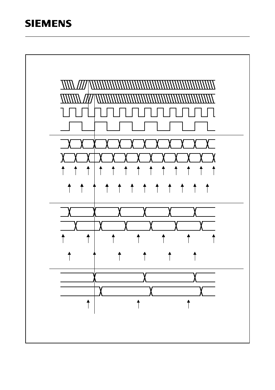
PEB 2055
PEF 2055
Application Hints
Semiconductor Group
123
Figure 43
CFI Bit Timing with Respect to the Framing Signal FSC (CMD1:CSS = 1)
ITT08058
PFS
PFS
RCL
RCL
TS0,
Bit 7
DD#
DD#
DU#
Conditions:
DU#
DD#
TS0, Bit 7
DD#
DU#
DU#
SIP#
(OUT)
(IN)
SIP#
CMD1: CSM =
1
0
=
CSM
:
CMD1
CFI Modes 0,
1 and 3
CFI Mode 2
0
=
CXF
:
CMD2
CMD2 : CXF = 1
0
=
CRR
:
CMD2
CMD2 : CRR = 1
1
=
CRR
:
CMD2
CMD2 : CRR = 0
1
=
CXF
:
CMD2
CMD2 : CXF = 0
0
=
CXF
:
CMD2
CMD2 : CXF = 1
0
=
CRR
:
CMD2
CFI Modes 1 and 2
CTAR
H
=0
2
CMD1
:
CSS
=
1
,2
0
=
H
CBSR
(FSC is frame sync.
source for the CFI)
CFI Mode 0
CBSR
H
=2
0
,
02
=
H
CTAR
CFI Mode 3
CBSR
H
=2
0
,
02
=
H
CTAR
(OUT)
SIP#
TS0, Bit 6
Bit 5
TS0,
Bit 4
TS0,
Bit 3
TS0,
Bit 7
TS0,
Bit 6
TS0,
Bit 5
TS0,
Bit 4
TS0,
TS0, Bit 4
TS0, Bit 5
TS0, Bit 6
TS0, Bit 7
TS0, Bit 7
TS0, Bit 6
TS0, Bit 5
TS0, Bit 4
TS0, Bit 7
TS0, Bit 6
TS0, Bit 7
Bit 6
TS0,
TS0, Bit 3
TS0, Bit 7
TS0, Bit 6
TS0,
Bit 0
TS0,
Bit 7
TS0,
Bit 0
TS0,
Bit 7
Bit 7
TS0,
TS0,
Bit 0
TS0,
Bit 0
Bit 6
TS0,
TS0,
Bit 5
TS0,
Bit 4
TS0,
Bit 3
TS0,
Bit 2
TS0,
Bit 1
TS0,
Bit 6
TS0,
Bit 5
TS0,
Bit 4
TS0,
Bit 3
TS0,
Bit 2
TS0,
Bit 1
TS0,
Bit 6
TS0,
Bit 5
TS0,
Bit 4
TS0,
Bit 3
TS0,
Bit 2
TS0,
Bit 1
TS0,
Bit 6
TS0,
Bit 5
TS0,
Bit 4
TS0,
Bit 3
TS0,
Bit 2
TS0,
Bit 1

PEB 2055
PEF 2055
Application Hints
Semiconductor Group
124
Examples
1) In CFI mode 0, with a frame consisting of 32 time slots, the following timing
relationship between the framing signal source PFS and the data signals is required:
Figure 44
Timing Signals for CFI Bit Shift Example 1
The framing signal source PFS shall mark CFI time slot 31, bit 1 in downstream direction
and CFI time slot 0, bit 5 in upstream direction. The data shall be transmitted and
sampled with the falling CRCL edge. The timing of the FSC and DCL output signals shall
be as shown in figure 44. The PFS signal is sampled with the rising PDC edge.
The following CFI register values result:
Since PFS marks the downstream bit 1, the CBSR:CDS bits must be set to "000",
according to table 18.
If the CBSR:CDS bits are set to "000", PFS marks the time slot TSN ≠ 1, according to
table 18.
PFS shall mark CFI time slot 31, i.e. TSN ≠ 1 = 31, or
TSN = 31 + 1 = (32)
mod 32
= 0
From this it follows that:
CTAR:TSN6 ... 0 = TSN + 2 = 0 + 2 = 2
D
= 0000010
B
; i.e. CTAR = 02
H
The upstream CFI frame shall be shifted by 4 bits to the left (TS31, bit 1 + 4 bits yields
in TS0, bit 5).
ITT08059
0
1
PFS
PDC/
DD#
DU#
FSC
DCL
CRCL
:
1
=
CSM
CMD1
Condition:
CFI Mode 0
PMOD PSM = 1
:
CMD2 CXF = 1
:
:
0
=
CRR
CMD2
CMD2 COC = 0
:
:
011
=
FC2
CMD2
...0
Bit 7
TS0,
TS31, Bit 2
TS31, Bit 1
TS31, Bit 0
Bit 6
TS0,
Bit 2
TS0,
Bit 3
TS0,
Bit 4
TS0,
TS0, Bit 5
Bit 6
TS0,

PEB 2055
PEF 2055
Application Hints
Semiconductor Group
125
The CBSR:CUS bits must therefore be set to "0100", according to figure 41.
The complete value for CBSR is: CBSR = 04
H
Finally, the CMD2 register bits must be set to
FC2 ... 0 = 011, COC = 0, CXF = 1, CRR = 0, CBN9 ... 8 = 00, i.e. CMD2 = 68
H
2) In CFI mode 0, with a frame consisting of 32 time slots, the following timing
relationship between the framing signal source FSC and the data signals is required:
Figure 45
Timing Signals for CFI Bit Shift Example 2
The framing signal source FSC shall mark CFI time slot 4, bit 1 in downstream direction
and CFI time slot 0, bit 5 in upstream direction. The data shall be transmitted with the
rising CRCL edge and sampled with the rising CRCL edge. The FSC signal shall be
sampled with the rising DCL edge.
The following CFI register values result:
Since FSC marks the downstream bit 1, the CBSR:CDS bits must be set to "000",
according to table 18.
If the CBSR:CDS bits are set to "000", FSC marks the time slot TSN ≠ 1, according to
table 18.
FSC shall mark CFI time slot 4, i.e. TSN ≠ 1 = 4, or TSN = 4 + 1 = 5
ITT08060
Start of Internal Frame
0
1
FSC
DCL
DD#
Bit 2
Bit 1
Bit 0
Bit 3
Bit 7
Bit 6
Bit 5
Time-Slot 4
Required
Offset in
Upstream
Direction
Downstream
Offset in
Required
Bit 3
Bit 4
Bit 5
Bit 6
Bit 7
Direction
Bit 2
DU#
CMD1 CSM = 1
:
CFI Mode 0
CMD2 CRR = 1
:
:
0
=
CXF
CMD2
TS0, Bit 5
Time-Slot 5
Time-Slot 0
Bit 1
TS4,

PEB 2055
PEF 2055
Application Hints
Semiconductor Group
126
From this it follows that:
CTAR:TSN6 ... 0 = TSN + 2 = 5 + 2 = 7
D
= 0000111
B
; i.e. CTAR = 07
H
The upstream CFI frame shall be shifted by 28 bits to the right (ts 4, bit 1 - 28 bits yields
in TS0, bit 5)
Since it is not possible to shift the upstream frame with respect to the downstream frame
by more than 15 bits when using the CBSR:CUS bits, the following trick must be used:
The CBSR:CUS bits are set to "0100" to shift the frame by 4 bits to the left. The
remaining shift to the right of 28 + 4 = 32 bits (equivalent to 4 time slots) can now be
performed by renumbering the upstream CFI time slots in the software. This results in
an offset of 4 time slots when addressing a CFI time slot via the Control Memory (CM):
If CFI time slot N shall be switched (N refers to the external time slot numbering), the CM
must be written with the CFI address (N + 4)
mod 32
.
If for example the upstream CFI time slot 0 of port 0 shall be switched to a PCM time slot,
the CM address 88
H
(CFI p 0, TS4) must be used.
The complete value for CBSR is: CBSR = 04
H
Finally the CMD2 register bits must be set to
FC2 ... 0 = XXX, COC = X, CXF = 0, CRR = 1, CBN9 ... 8 = 00, i.e.: CMD2 = 04
H
CFI Receive Line Selection CMD1:CIS1 ... CIS0
The CFI transmit line of a given logical port (as it is used for programming the switching
function) is always assigned to a dedicated physical transmit pin, e.g. in CFI mode 1, pin
DD1 carries the CFI data of logical port 1.
In receive direction however, an assignment between logical and physical ports can be
made in CFI modes 1 and 2. This selection is programmed via the alternative input
selection bits 1 and 0 (CIS1, CIS0) in the CMD1 register.
In CFI mode 0 and 3, CIS1 and CIS0 should both be set to 0.
In CFI mode 1, CIS0 selects between receive lines DU0 and DU2 for logical port 0 and
CIS1 between the receive lines DU1 and DU3 for logical port 1.
In CFI mode 2, CIS0 selects between the receive lines DU0 and DU2, CIS1 should be
set to 0.

PEB 2055
PEF 2055
Application Hints
Semiconductor Group
127
Table 19 shows the function taken over by each of the CFI interface pins, depending on
the CFI mode and the values programmed to CIS1 and CIS0.
Figure 46 shows the correlation between physical and logical CFI ports in CFI modes 0,
1, 2 and 3:
Figure 46
Correlation Between Physical and Logical CFI Ports
Table 19
CFI
Mode
Port 0
Port 1
Port 2
Port 3
DU0
DD0
DU1
DD1
DU2
DD2
DU3
DD3
0
IN0
OUT0
IN1
OUT1
IN2
OUT2
IN3
OUT3
1
IN0
CIS0 = 0
OUT0
IN1
CIS1 = 0
OUT1
IN0
CIS0 = 1
high Z
IN1
CIS1 = 1
high Z
2
IN
CIS0 = 0
OUT
≠
high Z
IN
CIS0 = 1
high Z
≠
high Z
3
I/O4
I/O0
I/O5
I/O1
I/O6
I/O2
I/O7
I/O3
ITS09549
DU0
DU2
Logical Ports:
IN0
OUT0
1
0
CMD1:
CIS0
OUT1
DD0
DD1
CIS1
CMD1:
0
1
IN1
DU3
DU1
EPIC
CFI Mode
Logical Ports:
OUT0
DD0
Physical
Pins:
DU0
IN0
IN1
DU1
OUT1
DD1
IN2
DU2
OUT2
DD2
IN3
DU3
OUT3
DD3
Pins:
Physical
DU0
DU2
IN
1
0
CMD1:
CIS0
DD0
OUT
Logical Ports:
SIP0
I/O0
Logical Ports:
Physical
Pins:
Physical
Pins:
I/O1
I/O2
I/O3
I/O4
I/O5
I/O6
I/O7
SIP1
SIP2
SIP3
SIP4
SIP5
SIP6
SIP7
0
1
CFI Mode
2
CFI Mode
3
CFI Mode
EPIC
EPIC
EPIC
R
R
R
R

PEB 2055
PEF 2055
Application Hints
Semiconductor Group
128
CFI subtime Slot Position CSCR
If a time slot assignment is programmed in the control memory (CM), the used control
memory code defines the channel bandwidth and the subchannel position at the PCM
interface (refer to chapter 5.4.2). The subchannel position at the configurable interface
however is defined on a per port basis in the Configurable interface SubChannel
Register CSCR.
The subchannel control bits SC#1 ... SC#0 specify separately for each logical port the
bit positions to be exchanged with the data memory (DM) when a connection with a
channel bandwidth as defined by the CM code has been established:
Table 21 shows the effect of the different subchannel control bits SC#1 ... SC#0 on the
CFI ports in each CFI mode:
Note: In CFI mode 1:SC21 = SC01; SC20 = SC00; SC31 = SC11; SC30 = SC10
In CFI mode 2:SC31 = SC21 = SC11 = SC01; SC30 = SC20 = SC10 = SC00
If for example at CFI port 1 a 16 kbit/s channel shall be switched to (or from) a CFI bit
position 5 ... 4 from (or to) any 2 bit subtime slot position at the PCM interface, a CM
code defining a channel bandwidth of 16 kbit/s and defining the subchannel position at
the PCM interface must be written to the CM code field of the involved 8 bit CFI time slot
(i.e. 0111, 0110, 0101 or 0100). In order to insert (or extract) bit positions 5 ... 4 of the
selected 8 bit CFI time slot, SC11 ... SC10 have to be set to 01. Once fixed to this value,
all time slot connections programmed on CFI port 1 are performed on bits 7 ... 0 for
64 kbit/s channels, bits 3 ... 0 for 32 kbit/s channels and bits 5 ... 4 for 16 kbit/s
channels.
Table 20
SC#1
SC#0
Bit Positions for CFI Subchannels Having a Bandwidth of
64 kbit/s
32 kbit/s
16 kbit/s
0
0
1
1
0
1
0
1
7 ... 0
7 ... 0
7 ... 0
7 ... 0
7 ... 4
3 ... 0
7 ... 4
3 ... 0
7 ... 6
5 ... 4
3 ... 2
1 ... 0
Table 21
SC#1
SC#0
CFI Mode
0
1
2
3
SC01
SC11
SC21
SC31
SC00
SC10
SC20
SC30
port 0
port 1
port 2
port 3
port 0
port 1
see note
see note
port
see note
see note
see note
ports 0 and 4
ports 1 and 5
ports 2 and 6
ports 3 and 7

PEB 2055
PEF 2055
Application Hints
Semiconductor Group
129
Since for each CFI time slot there is only one control memory location, only one
subchannel may be mapped to each CFI time slot. The remaining bits of such a partly
unused CFI time slot are inactive e.g. set to high impedance if OMDR:COS = 0.
Note that if an odd numbered CFI time slot is initialized as an IOM channel with switched
D channel, SC#1 ... SC#0 must be set to "00" because the D channel is located at bits
7 ... 6. In this case the remaining bits can still be used for C/I and monitor channel
applications (refer to chapter 5.5).
For more detailed information on subchannel switching refer to chapter 5.4.2.
CFI Standby Mode OMDR:CSB
In standby mode (OMDR:CSB = 0), the CFI output ports are set to high impedance and
the clock signals DCL and FSC, if programmed as outputs (CMD1:CSS = 0), are
switched off.
Note that the internal operation of the EPIC is not affected in standby mode, i.e. the
received CFI data is still read in and may still be processed by the EPIC (switched to
PCM or
Ķ
P, etc.)
In operational mode (OMDR:CSB = 1), the CFI output pins take over the function
programmed in the control memory and DCL and FSC deliver clock and framing output
signals (if CMD1:CSS = 0) as programmed in CMD1 and CMD2.
CFI Output Driver Selection OMDR:COS
The output drivers at the configurable interface (DD# or I/O#) can be programmed as
open drain or tristate drivers.
If programmed as open drain drivers (OMDR:COS = 1), external pull-up resistors
(connected to
V
DD
) are required in order to pull the output line to a high level if a logical
1 is being transmitted. For unassigned channels (e.g. control memory code "0000") the
EPIC transmits a logical 1. The maximum output current at a low voltage level of 0.45 V
is 7 mA, pull-up resistors down to 680
can thus be used.
If programmed as tristate drivers (OMDR:COS = 0), logical 0s and 1s are transmitted
with push-pull output drivers, whereas unassigned channels are set to high impedance.

PEB 2055
PEF 2055
Application Hints
Semiconductor Group
130
5.3
Data and Control Memories
5.3.1
Memory Structure
The EPIC memory is composed of the Control Memory (CM) and the Data Memory
(DM). Their structure is shown in figure 47.
The control memory refers to the Configurable Interface (CFI) such that for each CFI
time slot and for each direction (upstream and downstream) there is a 4 bit code field
and an 8 bit data field location.
The code field defines the function of the corresponding CFI time slot. A time slot, may
for example, be transparently switched through to the PCM interface (switched channel)
or it may serve as monitor, feature control, command/indication or signaling channel in
an IOM or SLD application (preprocessed channel) or it may be directly switched to the
Ķ
P interface (
Ķ
P channel).
The use of the data field depends on the function defined by the code field. If a CFI time
slot is defined as a switched channel, the data field is interpreted as a pointer to the data
memory and defines therefore to which PCM time slot the connection shall be made. For
preprocessed channels, the data field serves as a buffer for the command/indication or
signaling value. If a
Ķ
P channel is programmed, the data field content is directly
exchanged with the CFI time slot.
The data memory refers to the PCM interface such that for each upstream time slot
there is a 4 bit code field and an 8 bit data field location, whereas for each downstream
time slot there is only an 8 bit data field location.
The data field locations buffer the PCM data transmitted and received over the PCM
interface. The code field (tristate field) defines whether the upstream data field contents
should be transmitted in the associated PCM time slot or whether the time slot should
be switched to high impedance.

PEB 2055
PEF 2055
Application Hints
Semiconductor Group
131
Figure 47
EPIC
ģ
Memory Structure
5.3.2
Indirect Register Access
The control and data memories must be accessed by the
Ķ
P in order to initialize the CFI
and PCM interfaces for the required functionality, to program time slot assignments, to
access the control/signaling channels (IOM/SLD), etc.
This access is performed through indirect addressing using the memory access
registers MADR, MAAR, and MACR.
ITD08062
Code Field
Data Field
Control Memory
CFI
Frame
0
127
Up-
stream
stream
Down-
127
0
Code Field
Data Field
127
0
Frame
PCM
Up-
stream
0
127
Down-
stream
Data Memory

PEB 2055
PEF 2055
Application Hints
Semiconductor Group
132
Memory Access Data Register
read/write
reset value:
undefined
The Memory Access Data Register MADR contains the data to be transferred from or to
a memory location. The meaning and the structure of this data depends on the kind of
memory being accessed. If, for example, MADR contains a pointer to a PCM time slot,
the data must be encoded according to figure 48. If it contains a 4 bit C/I code the
structure would for example be "11 C/I 11". For accesses to 4 bit code fields only the 4
least significant bits of MADR are relevant.
Memory Access Address Register
read/write
reset value:
undefined
The Memory Access Address Register MAAR specifies the address of the memory
access. This address encodes a CFI time slot for control memory and a PCM time slot
for data memory accesses. Bit 7 of MAAR (U/D bit) selects between upstream and
downstream memory blocks.
Bits MA6 ... 0 encode the CFI or PCM port and time slot number according to figure 48.
Memory Access Control Register
read/write
reset value:
undefined
The Memory Access Control Register MACR selects the type of memory (control or data
memory), the type of field (data or code field) and the access mode (read or write) of the
register access. When writing to the control memory code field, MACR also contains the
4 bit code (CMC3 ... 0) defining the function of the addressed CFI time slot.
bit 7
bit 0
MADR
MD7
MD6
MD5
MD4
MD3
MD2
MD1
MD0
bit 7
bit 0
MAAR
U/D
MA6
MA5
MA4
MA3
MA2
MA1
MA0
bit 7
bit 0
MACR
RWS
MOC3
MOC2
MOC1
MOC3/
CMC3
CMC2
CMC1
CMC0

PEB 2055
PEF 2055
Application Hints
Semiconductor Group
133
Figure 48
Time Slot Encoding for the Different PCM and CFI Modes
Memory Access Time
Writing to MACR starts a memory write or read operation which takes a certain time.
During this time no further memory accesses may be performed i.e. the MADR, MAAR,
and MACR registers may not be written. The STAR:MAC bit indicates whether a memory
operation is still in progress (MAC = 1) or already completed (MAC = 0) and should
therefore be interrogated before each access.
ITD08063
U/D
Port# (0-3)
CFI Mode 0
PCM Mode 0
4 Duplex Ports
32 Tume-Slots/Port
64 Time-Slots/Port
2 Duplex Ports
U/D
U/D
2 Duplex Ports
64 Time-Slots/Port
128 Time-Slots/Port
1 Duplex Port
U/D
U/D
16 Time-Slots/Port
8 Bidirectional Ports
U/D : (1) / Downstream (0)
Port# (0-1)
Port# (0-1)
Port# (0-3)
Time-Slot# (0-31)
Time-Slot# (0-63)
Time-Slot# (0-63)
Time-Slot# (0-127)
Time-Slot# (0-15)
CFI Mode 1
CFI Mode 2
CFI Mode 3
PCM Mode 2
PCM Mode 1

PEB 2055
PEF 2055
Application Hints
Semiconductor Group
134
Since memory operations must be synchronized to the EPIC internal bus which is
clocked by the reference clock (RCL), the time required for an indirect register access
can be given as a multiple of RCL clock cycles. A "normal" access to a single memory
location, for example, takes a maximum of 9.5 RCL cycles which is approximately 2.4
Ķ
s
assuming a 4 MHz clock (e.g. CFI configured as standard IOM-2 interface).
Memory Access Modes
Access to memory locations is furthermore influenced by the operation mode set via the
Operation Mode Register OMDR. There are 4 modes which can be selected with the
OMDR:OMS1, OMS0 bits:
Operation Mode Register
read/write
reset value:
00
H
≠ The CM reset mode (OMS1 ... 0 = 00) is used to reset all locations of the control
memory code and data fields with a single command within only 256 RCL cycles. A
typical application is resetting the CM with the command MACR = 70
H
which writes
the contents of MADR (XX
H
) to all data field locations and the code "0000"
(unassigned channel) to all code field locations. A CM reset should be made after
each hardware reset. In the CM reset mode the EPIC does not operate normally i.e.
the CFI and PCM interfaces are not operational.
≠ The CM initialization mode (OMS1 ... 0 = 10) allows fast programming of the
Control Memory since each memory access takes a maximum of only 2.5 RCL cycles
compared to the 9.5 RCL cycles in the normal mode. Accesses are performed on
individual addresses specified by MAAR. The initialization of control/signaling
channels in IOM or SLD applications can, for example, be carried out in this mode
(see chapter 5.5.1). In the CM initialization mode the EPIC does also not work
normally.
≠ In the normal operation mode (OMS1 ... 0 = 11) the CFI and PCM interfaces are
operational. Memory accesses performed on single addresses (specified by MAAR)
take 9.5 RCL cycles. An initialization of the complete data memory tristate field takes
1035 RCL cycles.
≠ In test mode (OMS1 ... 0 = 01) the EPIC sustains normal operation. However
memory accesses are no longer performed on a specific address defined by MAAR,
but on all locations of the selected memory, the contents of MAAR (including the U/D
bit!) being ignored. This function can for example be used to program a PCM idle code
to all PCM ports and time slots with a single command.
bit 7
bit 0
OMDR
OMS1
OMS0
PSB
PTL
COS
MFPS
CSB
RBS

PEB 2055
PEF 2055
Application Hints
Semiconductor Group
135
5.3.3
Memory Access Commands
The memory access commands can be divided into the following four categories:
≠ Access to the Data Memory Data Field:
Ķ
P access to PCM frame
≠ Access to the Data Memory Code Field: PCM tristate control
≠ Access to the Control Memory Data Field: time slot assignment,
Ķ
P access to CFI
frame
≠ Access to the Control Memory Code Field: set-up of CFI time slot functionality
In the following chapters, these commands are explained in more detail.
5.3.3.1 Access to the Data Memory Data Field
The data memory (DM) data field buffers the PCM data transmitted (upstream block) and
received (downstream block) via the PCM interface. Normally this data is switched
transparently from or to the CFI and there is no need to access it from the
Ķ
P interface.
For some applications however it is useful to have a direct
Ķ
P access to the PCM frame.
When an upstream PCM time slot (or even subtime slot) is not switched from the CFI
(unassigned channel), it is possible to write a fixed value to the corresponding DM data
field location. This value will then be transmitted repeatedly in each PCM frame without
further
Ķ
P interaction (PCM idle code). If instead a continuous pattern should be sent,
the write access can additionally be synchronized to the frame by means of synchronous
transfer interrupts (see chapter 5.7).
Writing to an upstream DM data field location can also be restricted to a 2 or 4 bit subtime
slot. It is thus possible to have certain subtime slots of the same 8 bit time slot switched
from the CFI with the other subtime slots containing a PCM idle code. This restriction is
made via the Memory Operation Code (refer to table 22).
For test purposes the upstream DM data field contents can also be read back.
The downstream DM data field cannot be written to, it can only be read. Reading such
a location reflects the PCM data contained in the received PCM frame regardless of a
connection to the CFI having been established or not. The
Ķ
P can thus determine the
contents of received PCM time slots simply by reading the corresponding downstream
DM locations. This reading can, if required, also be synchronized to the frame by means
of synchronous transfer interrupts.

PEB 2055
PEF 2055
Application Hints
Semiconductor Group
136
The Procedure for Writing to the Upstream DM Data Field is
W:MADR = value to be transmitted in the PCM (sub)time slot
W:MAAR = address of the desired (upstream)
1)
PCM time slot encoded according to
figure 48
MOC3 ... 0 defines the bandwidth and the position of the subchannel according to
table 22.
The Procedure for Reading the DM Data Field is
W:MAAR = address of the desired PCM time slot encoded according to figure 48
W:MACR = 1000 0000
B
= 80
H
2)
wait for STAR:MAC = 0
R:MADR = value
Figure 49 illustrates the access to the Data Memory Data Field.
1)
The U/D bit of MAAR will implicitly be set to 1.
2)
When reading a DM data field location, all 8 bits are read regardless of the bandwidth selected by the MOC
bits.
bit 7
bit 0
W:MACR =
0
MOC3
MOC2
MOC1
MOC0
0
0
0
Table 22
MOC3 ... 0
Transferred Bits
Channel Bandwidth
0000
0001
0011
0010
0111
0110
0101
0100
≠
bits 7 ... 0
bits 7 ... 4
bits 3 ... 0
bits 7 ... 6
bits 5 ... 4
bits 3 ... 2
bits 1 ... 0
≠
64 kbit/s
32 kbit/s
32 kbit/s
16 kbit/s
16 kbit/s
16 kbit/s
16 kbit/s

PEB 2055
PEF 2055
Application Hints
Semiconductor Group
137
Figure 49
Access to the Data Memory Data Field
ITD08064
.
.
.
.
.
MA6
U/D
MAAR:
MA0
Data Field
127
0
Frame
PCM
Up-
stream
0
127
Down-
stream
Data Memory
MADR:
U/D = 1
U/D = 0
MD0
MD7
.
.
.
.
.
RWS
0
MACR:
.
0
0
MOC 3 ... 0

PEB 2055
PEF 2055
Application Hints
Semiconductor Group
138
Examples
In PCM mode 0 the idle code "1010 0101
B
" shall be transmitted in time slot 16 of port 0:
W:MADR
=
1010 0101
B
; idle code
W:MAAR
=
1100 0000
B
; address of upstream PCM time slot 16 of port 0
according to figure 48
W:MACR
=
0000 1000
B
: write access, MOC code "0001"
The idle code can, of course, only be transmitted on the TxD# line if the corresponding
tristate bits are enabled (refer to chapter 5.3.3.2):
W:MADR
=
XXXX 1111
B
; all 8 bits of addressed time slot to low impedance
W:MAAR
=
1100 0000
B
; address of upstream PCM time slot 16 of port 0
according to figure 48
W:MACR
=
0110 0000
B
: write access, MOC code "1100"
For test purposes the idle code can also be read back:
W:MAAR
=
1100 0000
B
; address of upstream PCM time slot 16 of port 0
according to figure 48
W:MACR
=
10XX X000
B
: read access, MOC code "0XXX"
wait for STAR:MAC = 0
R:MADR
=
1010 0101
B
; idle code
In PCM mode 2 the idle pattern "0110" shall be transmitted in bit positions 3 ... 0 of time
slot 63, bits 7 ... 4 shall be tristated:
W:MADR
=
XXXX 0110
B
; idle code
W:MAAR
=
1011 1111
B
; address of upstream PCM time slot 63
according to figure 48
W:MACR
=
0001 0000
B
; write access, MOC code "0010"
Programming of the desired tristate functions:
W:MADR
=
XXXX 0011
B
; bits 7 ... 4 to high impedance, bits 3 ... 0 to low
impedance
W:MAAR
=
1011 1111
B
; address of upstream PCM time slot 63
according to figure 48
W:MACR
=
0110 0000
B
; write access, MOC code "1100"

PEB 2055
PEF 2055
Application Hints
Semiconductor Group
139
5.3.3.2 Access to the Data Memory Code (Tristate) Field
The data memory code field exists only for the upstream DM block and is also called the
PCM tristate field. Each (sub)time slot of each PCM transmit port can be individually
tristated via these code field locations.
If a (sub)time slot is set to low impedance, the contents of the corresponding DM data
field location is transmitted with a push-pull driver onto the transmit port TxD# and the
tristate control line TSC# is pulled low for the duration of that (sub)time slot.
If a (sub)time slot is set to high impedance, the transmit port TxD# will be tristated and
the TSC# line is pulled high for the duration of that (sub)time slot.
There are 4 code bits for selecting the tristate function of each 8 bit time slot i.e. 1 control
bit for each 16 kbit/s (2 bits) subtime slot. If a control bit is set to 1, the corresponding
subtime slot is set to low impedance, if it is set to 0 the subtime slot is tristated.
Figure 50 illustrates this behavior.
Figure 50
Tristate Control at the PCM Interface
The tristate field can be written to and, for test purposes, also be read back.
There are two commands (Memory Operation Codes) for accessing the tristate field:
With the "Single Channel Tristate Control" command (MOC3 ... 0 = 1100) the tristate
field of a single PCM time slot can be written to and also read back. The 4 least
significant bits of MADR are exchanged with the code field of the time slot selected by
the MAAR register.
With the "Tristate Control Reset" command (MOC3 ... 0 = 1101) the tristate field of all
PCM time slots can be written to with a single command. The 4 bits of MADR are then
copied to all code field locations regardless of the address programmed to MAAR. Such
a complete access to the DM tristate field takes 1035 RCL cycles.
ITD08065
X X X X 0 1 1 0
0
1
0
0
1
1
0
1
0
0
1
1
1
0
1
0
0
0
0
0
1
1
1
1
N
N+1
N+2
N+3
High Z
1 -
0 -
PCM Time-Slot#
DM Data Field
DM Tristate Field
TxD#
1
0
X
X
1
1
X
X
X
X
X
X
X
X
X
X
TSC#
0 -
1 -

PEB 2055
PEF 2055
Application Hints
Semiconductor Group
140
The MADR bits MD7 ... MD0 control the PCM time slot bit positions 7 ... 0 in the
following way:
MD7 ... MD4 are not used (don't care);
MD3 ... MD0 select between the states high impedance (MD# = 0) or low impedance
(MD# = 1)
The Procedure for Writing to a Single PCM Tristate Field is
W:MADR
= X X X X MD3 MD2 MD1 MD0
B
W:MAAR
= address of the desired (upstream)
1)
PCM time slot according to figure
48
W:MACR
= 0110
000
B
= 60
H
The Procedure for Reading Back a (Single) PCM Tristate Field Location is
W:MAAR
= address of the desired (upstream)
1)
PCM time slot according to figure 48
W:MACR
= E0
H
wait for STAR:MAC = 0
R:MADR
=
X X X X MD3 MD2 MD1 MD0
B
The Procedure for Writing to all PCM Tristate Field Positions is
W:MADR
=
X X X X MD3 MD2 MD1 MD0
B
W:MACR
=
0110 1000
B
= 68
H
1)
The U/D bit of MAAR will implicitly be set to 1.
time slot Bit Position:
7
6
5
4
3
2
1
0
MADR Bits:
MD3
MD2
MD1
MD0

PEB 2055
PEF 2055
Application Hints
Semiconductor Group
141
Figure 51 illustrates the access to the tristate field:
Figure 51
Access to the Data Memory Code (Tristate) Field
Examples
All PCM time slots shall be set to high impedance (disabled):
W:MADR
=
00
H
; all bits to high impedance
W:MACR
=
68
H
; write access with MOC = 1101
All PCM time slots shall be set to low impedance (enabled):
W:MADR
=
FF
H
; all bits to low impedance
W:MACR
=
68
H
; write access with MOC = 1101
In PCM mode 1, bits 7 ... 6 and 1 ... 0 of PCM port 1, time slot 10 shall be set to low
impedance, bits 5 ... 2 to high impedance:
W:MADR
=
0000 1001
B
; bits 7 ... 6 and 1 ... 0 to low impedance, bits 5 ... 2
to high impedance
W:MAAR
=
1010 1010
B
; address of upstream PCM port 1, time slot 10
according to figure 48
W:MACR
=
0110 0000
B
; write access with MOC = 1100
ITD08066
.
.
.
.
.
MA6
U/D
MAAR:
MA0
Code Field
Frame
PCM
Up-
stream
0
127
Data Memory
MADR:
U/D = 1
MD0
RWS
0
MACR:
0
0
MD1
MD2
MD3
X
X
X
X
1 0
0/1
1

PEB 2055
PEF 2055
Application Hints
Semiconductor Group
142
For test purposes this setting shall be read back:
W:MAAR
=
1010 1010
B
; address of upstream PCM port 1, time slot 10
according to figure 48
W:MACR
=
1110 0000
B
= E0
H
; read access with MOC = 1100
wait for STAR:MAC = 0
R:MADR
=
XXXX 1001
B
; read back of MD3 ... 0
5.3.3.3 Access to the Control Memory Data Field
Writing to or reading the control memory (CM) data field may serve different purposes
depending on the function given to the corresponding CFI time slot which is defined by
the 4 bit code field value:
There are two types of commands which give access to the CM data field:
The memory operation code MACR:MOC = 111X is used for writing to the CM data field
and code field simultaneously. The MADR content is transferred to the data field while
the MACR:CMC3 ... 0 bits are transferred to the code field. This command is explained
in more detail in chapter 5.3.3.4.
The memory operation code MACR:MOC = 1001 is used for reading or writing to the CM
data field. Since the CM code field is not affected, this command makes only sense if the
related CFI time slot has already the desired functionality.
The Procedure for Writing to the CM Data Field (using the MOC = 1001 command)
is
W:MADR
=
value
W:MADR
=
CFI time slot address according figure 48
R:MADR
=
0100 1000
B
= 48
H
The Procedure for Reading the CM Data Field is
W:MAAR
=
CFI time slot address according figure 48
W:MACR
=
1100 1000
B
= C8
H
wait for STAR:MAC = 0
R:MADR
=
value
Table 23
CFI Time Slot Application
Meaning of CM Data Field
Switched channel
Preprocessed channel
Ķ
P channel
Pointer to PCM interface
C/I or SIG value
CFI idle code

PEB 2055
PEF 2055
Application Hints
Semiconductor Group
143
Figure 52 illustrates this behavior.
Figure 52
Access to the Control Memory Data Field
ITD08067
.
.
.
.
.
MA6
U/D
MAAR:
MA0
Data Field
127
0
Frame
CFI
Up-
stream
0
127
Down-
stream
Control Memory
MADR:
U/D = 1
U/D = 0
MD0
MD7
.
.
.
.
.
RWS
0
MACR:
.
0
0
0
0
1
1

PEB 2055
PEF 2055
Application Hints
Semiconductor Group
144
Examples
In CFI mode 2, CFI time slot 123 has been initialized as a switched channel. The CM
data field value therefore represents a pointer to the PCM interface.
In a first step, the involved upstream and downstream PCM time slots shall be
determined:
W:MAAR
=
1111 1011
B
; address of upstream CFI time slot 123
W:MACR
=
1100 1000
B
; read back command
wait for STAR:MAC = 0
R:MADR
=
value
; encoded according figure 48
W:MAAR
=
0111 1011
B
; address of downstream CFI time slot 123
W:MACR
=
1100 1000
B
; read back command
wait for STAR:MAC = 0
R:MADR
=
value
; encoded according figure 48
In the next step a new time slot assignment (to PCM port 1, time slot 34, PCM mode 1)
shall be made for the upstream connection:
W:MADR
=
1100 0110
B
; upstream PCM time slot 34, port 1
W:MAAR
=
1111 1011
B
; address of upstream CFI time slot 123
W:MACR
=
0100 1000
B
; write command
5.3.3.4 Access to the Control Memory Code Field
The 4 bit code field of the control memory (CM) defines the functionality of a CFI time
slot and thus the meaning of the corresponding data field.
There are codes for switching applications, preprocessed applications and for direct
Ķ
P
access applications (see table 24).
This 4 bit code, written to the MACR:CMC3 ... 0 bit positions, will be transferred to the
CM code field by selecting MACR:MOC = 111X. The 8 bit MADR value is at the same
time transferred to the CM data field.
The Procedure for Writing to the CM Code and Data Fields with a Single
Command is
W:MADR = value for data field
W:MAAR = CFI time slot address encoded according to figure 48
CMC3 ... 0 CM code, refer to table 24
bit 7
bit 0
W:MACR =
0
1
1
1
CMC3
CMC2
CMC1
CMC0

PEB 2055
PEF 2055
Application Hints
Semiconductor Group
145
Figure 53 illustrates this behavior.
Figure 53
Write Access to the Control Memory Data and Code Fields
For reading back the CM code field, the command MACR:MOC = 111X is also used, the
value of CMC3 ... 0 being don't care. The code field value can then be read from the
lower 4 bits of MADR.
ITD08068
.
.
MA6
U/D
MACR:
Data Field
Control Memory
MADR:
U/D = 1
U/D = 0
MD0
MD7
.
.
.
.
.
MAAR:
.
Code Field
stream
Down-
127
0
stream
Up-
CFI
Frame
0
127
0
...
3
CMC
.
.
. MA0
1
1
1
0

PEB 2055
PEF 2055
Application Hints
Semiconductor Group
146
The Procedure for Reading the CM Code is
W:MAAR
=
CFI time slot address encoded according to figure 48
W:MACR
=
1111 XXXX
B
wait for STAR:MAC = 0
CMC3 ... 0: CM code, refer to table 24
Figure 54 illustrates this behavior.
Figure 54
Read Access to the Control Memory Code Field
bit 7
bit 0
R:MADR =
X
X
X
X
CMC3
CMC2
CMC1
CMC0
ITD08069
.
.
MA6
U/D
MACR:
Control Memory
MADR:
U/D = 1
U/D = 0
MD0
MAAR:
Code Field
stream
Down-
127
0
stream
Up-
CFI
Frame
0
127
.
.
. MA0
1
1
1
X
X
1
X
X
X
X
X
X
MD1
MD2
MD3

PEB 2055
PEF 2055
Application Hints
Semiconductor Group
147
Table 24 shows all available Control Memory codes.
Examples
In CFI mode 2, CFI time slot 123 shall be initialized as a switched channel. The CM data
field value therefore represents a pointer to the PCM interface.
In a first step, a time slot assignment to PCM port 1, time slot 34 (PCM mode 1) shall be
made for a 64 kbit/s upstream connection:
W:MADR
=
1100 0110
B
; upstream PCM time slot 34, port 1
W:MAAR
=
1111 1011
B
; address of upstream CFI time slot 123
W:MACR
=
0111 0001
B
; write data + code field command, code "0001"
In a next step, the bandwidth of the previously made connection shall be verified:
W:MAAR
=
1111 1011
B
; address of upstream CFI time slot 123
W:MACR
=
1111 0000
B
; read back code field command
wait for STAR:MAC = 0
R:MADR
=
XXXX 0001
B
; the code "0001" (64 kbit/s channel) is read back
Table 24
Application
CMC3 ... 0
Transferred Bits
Channel Bandwidth
Disable connection
Switched 8 bit channel
Switched 4 bit channel
Switched 4 bit channel
Switched 2 bit channel
Switched 2 bit channel
Switched 2 bit channel
Switched 2 bit channel
0000
0001
0011
0010
0111
0110
0101
0100
≠
bits 7 ... 0
bits 7 ... 4
bits 3 ... 0
bits 7 ... 6
bits 5 ... 4
bits 3 ... 2
bits 1 ... 0
unassigned
64 kbit/s
32 kbit/s
32 kbit/s
16 kbit/s
16 kbit/s
16 kbit/s
16 kbit/s
Preprocessed channel
Preprocessed channel
Preprocessed channel
1000
1010
1011
refer to chapter 5.5
Ķ
P channel
1001
refer to chapter 5.6
and chapter 5.7

PEB 2055
PEF 2055
Application Hints
Semiconductor Group
148
Tristate Behavior at the Configurable Interface
The downstream control memory code field, together with the CSCR and OMDR
registers also defines the state of the output driver at the downstream CFI ports.
Unassigned channels (code "0000") are set to the inactive state. Subchannels (codes
"0010" to "0111") are only active during the subtime slot position specified in CSCR. The
OMDR:COS bit selects between tristate outputs and open drain outputs:
Figure 55 illustrates this behavior in case of tristate outputs:
Figure 55
Tristate Behavior at the CFI
1)
An external pull-up resistor is required to establish a high voltage level.
Table 25
Logical State
Tristate Outputs
Open Drain Outputs
Logical 0
Logical 1
Inactive
Low voltage level
High voltage level
High impedance
Low voltage level
Not driven
1)
Not driven
1)
ITD08070
X X X X X X X X
Pointer to DM
Pointer to DM
0
1
0
0
1
1
0
1
0
0
0
0
1
0
0
0
0
1
1
0
1
0
0
1
N
N+1
N+2
N+3
Unassigned
Channel
64 kbit/s Channel
(Switched from PCM)
16 kbit/s Channel
CSCR : SC#1..#0 = 01
(Switched from PCM)
ĶP Channel
(Always 64 kbit/s)
High Z
1 -
0 -
CFI Time-Slot #
CM Data Field
CM Code Field
DD #

PEB 2055
PEF 2055
Application Hints
Semiconductor Group
149
Table 26
Summary of Memory Operations
Application
MADR
MAAR
MACR (Hex)
Writing a PCM idle value to
the upstream DM data field
The MACR value specifies
the bandwidth and bit
position at the PCM
interface
8 bit, 4 bit or 2 bit idle
value to be transmitted
at the PCM interface
Address of the
(upstream) PCM
port and time
slot
08
H
(bits 7 ... 0)
18
H
(bits 7 ... 4)
10
H
(bits 3 ... 0)
38
H
(bits 7 ... 6)
30
H
(bits 5 ... 4)
28
H
(bits 3 ... 2)
20
H
(bits 1 ... 0)
Reading the up- or
downstream DM data field
8 bit value transmitted
at the upstream or 8 bit
value received at the
downstream PCM
interface
Address of the
PCM port and
time slot
88
H
Writing to a single tristate
field location
Tristate information
contained in the
4 LSBs:
0 = tristated,
1 = active
Address of the
(upstream) PCM
port and time
slot
60
H
Writing to all tristate field
locations
Tristate information
contained in the
4 LSBs:
0 = tristated,
1 = active
Don't care
68
H
Reading a single tristate
field location
Tristate information
contained in the 4
LSBs
Address of the
(upstream) PCM
port and time
slot
E0
H
Writing to the CM data field 8 bit value
(C/I value, pointer to
PCM interface, etc.)
Address of the
CFI port and
time slot
48
H

PEB 2055
PEF 2055
Application Hints
Semiconductor Group
150
Reading the CM data field 8 bit value
(C/I value, pointer to
PCM interface, etc.)
Address of the
CFI port and
time slot
C8
H
Reading the CM code field 4 bit code contained in
the 4 LSBs
Address of the
CFI port and
time slot
F0
H
Writing a switching code to
the CM
The MACR value specifies
the bandwidth and bit
position at the PCM
interface
Pointer to DM:
PCM port and
time slot
Address of the
CFI port and
time slot
70
H
(unassigned)
71
H
(bits 7 ... 0)
73
H
(bits 7 ... 4)
72
H
(bits 3 ... 0)
77
H
(bits 7 ... 6)
76
H
(bits 5 ... 4)
75
H
(bits 3 ... 2)
74
H
(bits 1 ... 0)
Writing the "
Ķ
P channel"
code to the CM
8 bit idle value
Address of the
CFI port and
time slot
79
H
Writing a "preprocessed
channel" code to the CM
refer to figure 68
refer to
figure 68
refer to
figure 68
Table 26
Summary of Memory Operations
Application
MADR
MAAR
MACR (Hex)

PEB 2055
PEF 2055
Application Hints
Semiconductor Group
151
5.4
Switched Channels
This chapter treats the switching functions between the CFI and PCM interfaces which
are programmed exclusively in the control memory. The switching functions of channels
which involve the
Ķ
P interface or which are programmed in the synchronous transfer
registers are treated in chapter 5.6 and chapter 5.7.
The EPIC is a non-blocking space and time switch for 128 channels per direction.
Switching is performed between the configurable (CFI) and the PCM interfaces. Both
interfaces provide up to 128 time slots which can be split up into either 4 ports with up to
32 time slots, 2 ports with up to 64 time slots or 1 port with up to 128 time slots. In all of
these cases each port consists of a separate transmit and receive line (duplex ports). On
the CFI side a bidirectional mode is also provided (CFI mode 3) which offers 8 ports with
up to 16 time slots per port. In this case each time slot of each port can individually be
programmed to be either input or output.
The time slot numbering always ranges from 0 to N ≠ 1 (N = number of time slots/frame),
and each time slot always consists of 8 contiguous bits. The bandwidth of a time slot is
therefore always 64 kbit/s.
The EPIC can switch single time slots (64 kbit/s channels), double time slots (128 kbit/s
channels) and also 2 bit and 4 bit wide subtime slots (16 and 32 kbit/s channels). The
bits in a time slot are numbered 7 through 0. On the serial interfaces (PCM and CFI),
bit 7 is the first bit to be transmitted or received, bit 0 the last. If the
Ķ
P has access to the
serial data, bit 7 represents the MSB (D7) and bit 0 the LSB (D0) on the
Ķ
P bus.
The switching of 128 kbit/s channels implies that two consecutive time slots starting with
an even time slot number are used, e.g. PCM time slots 22 and 23 can be switched as
a single 16 bit wide time slot to CFI time slots 4 and 5. Under these conditions it is
guaranteed that the involved time slots are submitted to the same frame delay (also refer
to chapter 5.4.4).
The switching of channels with a data rate of 16 and 32 kbit/s is possible for the following
subtime slot positions within an 8 bit time slot:

PEB 2055
PEF 2055
Application Hints
Semiconductor Group
152
5.4.1
CFI - PCM Time Slot Assignment
All time slot assignments are programmed in the control memory (CM). Each line
(address) of the CM refers to one CFI time slot. The MAAR register, which is used to
address the CM, therefore specifies the CFI port and time slot to be switched. The data
field of the CM contains a pointer which points to a location in the data memory (DM).
The data memory contains the actual PCM data to be switched. The MADR register
contains the data to be copied to the CM data field. Since this data is interpreted as a
pointer to the DM, the MADR contents therefore specifies the PCM port and time slot to
be switched. The 4 bit CM code field must finally contain a value to declare the
corresponding CFI time slot as a switched channel (codes with a leading 0). This code
must be written at least once to the CM using the MACR register.
Since the CFI - PCM time slot assignment is programmed at the CFI side, it is possible
to switch a single downstream PCM time slot to several downstream CFI time slots. It is,
however, not possible to switch a single upstream CFI time slot to several upstream
PCM time slots.
If several upstream 64 kbit/s CFI time slots are assigned to the same upstream 64 kbit/s
PCM time slot, only the data of one CFI time slot will actually be switched since each
upstream connection will simply overwrite the DM data field. This switching mode can
therefore only effectively be used if the upstream switching is performed on different
subtime slot locations within the same PCM time slot (refer to chapter 5.4.2).
The following sequences can be used to program, verify, and cancel a CFI - PCM time
slot connection:
8 bit time slot:
7
6
5
4
3
2
1
0
32 kbit/s channel
7
6
5
4
32 kbit/s channel
3
2
1
0
16 kbit/s channel
7
6
16 kbit/s channel
5
4
16 kbit/s channel
3
2
16 kbit/s channel
1
0

PEB 2055
PEF 2055
Application Hints
Semiconductor Group
153
Programming of a 64 kbit/s CFI - PCM Time Slot Connection
≠ in case the CM code field has not yet been initialized with a switching code:
W:MADR
=
PCM port and time slot encoded according to figure 48
W:MAAR
=
CFI port and time slot encoded according to figure 48
W:MACR
=
0111 0001
B
= 71
H
≠ in case the CM code field has already been initialized with a switching code:
W:MADR
=
PCM port and time slot encoded according to figure 48
W:MAAR
=
CFI port and time slot encoded according to figure 48
W:MACR
=
0100 1000
B
= 48
H
Enabling the PCM Output Driver for a 64 kbit/s Time Slot
W:MADR
=
XXXX 1111
B
= XF
H
W:MAAR
=
PCM port and time slot encoded according to figure 48
W:MACR
=
0110 0000
B
= 60
H
Reading Back a Time Slot Assignment of a Given CFI Time Slot
≠ reading back the PCM time slot involved:
W:MAAR
=
CFI port and time slot encoded according to figure 48
W:MACR
=
1100 1000
B
= C8
H
wait for STAR:MAC = 0
R:MADR
=
PCM port and time slot encoded according to figure 48
≠ reading back the involved bandwidth and PCM subtime slot position:
W:MAAR
=
CFI port and time slot encoded according to figure 48
W:MACR
=
1111 0000
B
= F0
H
wait for STAR:MAC = 0
R:MADR
=
XXXX code; 4 bit bandwidth code encoded according to table 24
Cancelling of a Programmed CFI - PCM Time Slot Connection
W:MADR
=
don't care
W:MAAR
=
CFI port and time slot encoded according to figure 48
W:MACR
=
0111 0000
B
= 70
H
; code "0000" (unassigned channel)
Disabling the PCM Output Driver
W:MADR
=
XXXX 0000
B
= X0
H
W:MAAR
=
PCM port and time slot encoded according to figure 48
W:MACR
=
0110 0000
B
= 60
H

PEB 2055
PEF 2055
Application Hints
Semiconductor Group
154
Examples
In PCM mode 1 and CFI mode 3 the following connections shall be programmed:
Upstream: CFI port 5, time slot 7, bits 7 ... 0 to PCM port 0, time slot 12, bits 7 ... 0
W:MADR
=
1001 1000
B
; PCM time slot encoding according to figure 48
W:MAAR
=
1011 1011
B
; CFI time slot encoding according to figure 48
W:MACR
=
0111 0001
B
; CM code for switching a 64 kbit/s channel
(code "0001")
Downstream: CFI port 4, time slot 2, bits 7 ... 0 from PCM port 1, time slot 3, bits 7 ... 0
W:MADR
=
0000 0111
B
; PCM time slot encoding according to figure 48
W:MAAR
=
0001 1000
B
; CFI time slot encoding according to figure 48
W:MACR
=
0111 0001
B
; CM code for switching a 64 kbit/s channel (0001)
The following sequence sets transmit time slot 12 of PCM port 0 to low impedance:
W:MADR
=
0000 1111
B
; all bits to low Z
W:MAAR
=
1001 1011
B
; PCM time slot encoding according to figure 48
W:MACR
=
0110 0000
B
; MOC code "1100" to access the tristate field

PEB 2055
PEF 2055
Application Hints
Semiconductor Group
155
After these three programming steps, the EPIC memories will have the following
contents:
Figure 56
Memory Content of the EPIC
ģ
for a CFI - PCM Time Slot Connection
ITD08071
1 0 0 1 1 0 0 0
1
0
0
0
Code Field
Data Field
Control Memory
CFI
Frame
0
127
Up-
stream
stream
Down-
1
1
1
0
0
0
0
0
127
0
0
0
0 1
Code Field
Data Field
1 1 1 1
127
0
Frame
PCM
Up-
stream
0
127
Down-
stream
Data Memory
P5, TS7
P4, TS2
P0, TS12
P1, TS3

PEB 2055
PEF 2055
Application Hints
Semiconductor Group
156
5.4.2
Subchannel Switching
The switching of subchannels is programmed by first specifying the time slot (which is
always 8 bits wide) to be switched, then by restricting the actual switching operation to
the desired bandwidth and subtime slot position. The switching function for an (8 bit) CFI
time slot is programmed in the control memory (CM) by writing a pointer that points to
an (8 bit) PCM time slot to the corresponding data field location. The MADR register
contains the pointer (PCM time slot) and the MAAR register is used to specify the CFI
time slot.
The "8 bit" connection can now be restricted to the desired 4 or 2 bit connection by
selecting an appropriate control memory code. The code is programmed via
MACR:CMC3 ... 0. These subchannel codes perform two functions: they specify the
bandwidth (actual number of bits to be switched) and the location of the subtime slot
within the selected (8 bit) PCM time slot. The location of the subtime slot within the
selected (8 bit) CFI time slot is predefined by the setting of the CSCR register. Each CFI
port can be set to a different subtime slot mode. In each mode a certain relationship
exists between programmed bandwidth (which can still be individually selected for each
CFI time slot) and the occupied bit positions within the time slot (which is fixed for each
CFI port by the CSCR register).
It should be noted that only one subtime slot can exist within a given CFI time slot. On
the PCM side however each time slot may be split up into 2
◊
4 bits, 4
◊
2 bits or any
mixture of these.
The CSCR register has the following format:
CFI Subchannel Register
read/write
reset value:
00
H
Below, all possible combinations of subchannel switching between the CFI and PCM
interfaces are shown:
bit 7
bit 0
CSCR
SC31
SC30
SC21
SC20
SC11
SC10
SC01
SC00
PEB 2055
PEF 2055
Application Hints
Semiconductor Group
157
Subchannel selection SC#1 ... SC#0 = 00:
Subchannel selection SC#1 ... SC#0 = 01:
CM code
CFI subchannel position
switched
to or from
PCM subchannel position
CFI time slot
PCM time slot
0001
7
6
5
4
3
2
1
0
7
6
5
4
3
2
1
0
0011
7
6
5
4
7
6
5
4
0010
7
6
5
4
3
2
1
0
0111
7
6
7
6
0110
7
6
5
4
0101
7
6
3
2
0100
7
6
1
0
CM code
CFI subchannel position
switched
to or from
PCM subchannel position
CFI time slot
PCM time slot
0001
7
6
5
4
3
2
1
0
7
6
5
4
3
2
1
0
0011
3
2
1
0
7
6
5
4
0010
3
2
1
0
3
2
1
0
0111
5
4
7
6
0110
5
4
5
4
0101
5
4
3
2
0100
5
4
1
0

PEB 2055
PEF 2055
Application Hints
Semiconductor Group
158
Subchannel selection SC#1 ... SC#0 = 10:
Subchannel selection SC#1 ... SC#0 = 11:
CM code
CFI subchannel position
switched
to or from
PCM subchannel position
CFI time slot
PCM time slot
0001
7
6
5
4
3
2
1
0
7
6
5
4
3
2
1
0
0011
7
6
5
4
7
6
5
4
0010
7
6
5
4
3
2
1
0
0111
3
2
7
6
0110
3
2
5
4
0101
3
2
3
2
0100
3
2
1
0
CM code
CFI subchannel position
switched
to or from
PCM subchannel position
CFI time slot
PCM time slot
0001
7
6
5
4
3
2
1
0
7
6
5
4
3
2
1
0
0011
3
2
1
0
7
6
5
4
0010
3
2
1
0
3
2
1
0
0111
1
0
7
6
0110
1
0
5
4
0101
1
0
3
2
0100
1
0
1
0

PEB 2055
PEF 2055
Application Hints
Semiconductor Group
159
Examples
In PCM mode 0 and CFI mode 0 the following connections shall be programmed:
Upstream: CFI port 0, time slot 3, bits 1 ... 0 to PCM port 0, time slot 4, bits 1 ... 0
W:MADR =
1001
0000
B
PCM time slot encoding, the subchannel position is
defined by MACR:CMC3 ... 0 = 0100
W:MAAR
=
1000 1001
B
CFI time slot encoding, the subchannel position is
defined by CSCR:SC01 ... 00 = 11
W:MACR
=
0111 0100
B
CM code for switching a 16 kbit/s/bits 1 ... 0
channel (0100)
Upstream: CFI port 3, time slot 7, bits 3 ... 2 to PCM port 0, time slot 4, bits 5 ... 4
W:MADR
=
1001 0000
B
PCM time slot encoding, the subchannel position is
defined by MACR:CMC3 ... 0 = 0110
W:MAAR
=
1001 1111
B
CFI time slot encoding, the subchannel position is
defined by CSCR:SC31 ... 30 = 10
W:MACR
=
0111 0110
B
CM code for switching a 16 kbit/s, bits 3 ... 2
channel (0110)
The following sequence sets transmit time slot 4 of PCM port 0 bits 5 ... 4 and 1 ... 0 to
low impedance and bits 7 ... 6 and 3 ... 2 to high impedance:
W:MADR
=
0000 0101
B
bits 5, 4, 1, 0 to low Z and bits 7, 6, 3, 2 to high Z
W:MAAR
=
1001 0000
B
PCM time slot encoding
W:MACR
=
0110 0000
B
MOC code to access the tristate field
Downstream: CFI port 2, time slot 7, bits 3 ... 0 from PCM port 1, time slot 3, bits 7 ... 4
W:MADR
=
0000 1011
B
PCM time slot encoding, the subchannel position is
defined by MACR:CMC3 ... 0 = 0011
W:MAAR
=
0001 1101
B
CFI time slot encoding, the subchannel position is
defined by CSCR:SC21 ... 20 = 01
W:MACR
=
0111 0011
B
CM code for switching a 32 kbit/s/bits 7 ... 4
channel (0011)

PEB 2055
PEF 2055
Application Hints
Semiconductor Group
160
Downstream: CFI port 2, time slot 10, bits 5 ... 4 from PCM port 0, time slot 4, bits 7 ... 6
W:MADR
=
0001 0000
B
PCM time slot encoding, the subchannel position is
defined by MACR:CMC3 ... 0 = 0111
W:MAAR
=
0010 1100
B
CFI time slot encoding, the subchannel position is
defined by CSCR:SC21 ... 20 = 01
W:MACR
=
0111 0111
B
CM code for switching a 16 kbit/s/bits 7 ... 6
channel (0111)
Finally the CSCR register has to be programmed to define the subchannel positions at
the CFI:
W:CSCR = 1001 XX11
B
port 0: bits 1 ... 0 or 3 ... 0; port 1: not used in this
example;
port 2: bits 5 ... 4 or 3 ... 0; port 3: bits 3 ... 2 or 7 ... 4
After these three programming steps, the EPIC memories will have the following content:
Figure 57
Memory Content in Case of CFI - PCM Subchannel Connections
ITD08072
1 0 0 1
0 0 0
1 0
0
Code Field
Data Field
Control Memory
CFI
Frame
0
127
Up-
stream
stream
Down-
1
1
1 0
0
0
0
0
127
0
0
0
1
Code Field
Data Field
127
0
Frame
PCM
Up-
stream
0
127
Down-
stream
Data Memory
P0, TS3
Bits 1, 0
0 1
0
0
0
1
0
0
1
Bits 3, 2
P3, TS7
1
0
0
0
0
1
0
0 1
Bits 7, 4
P1, TS3
P0, TS4
- -
-
-
P0, TS4
Bits 7, 6
1
1 1
0
0 0 0
0
1
1
0
0
0
P2, TS7
Bits 3, 0
P2, TS10
Bits 5, 4

PEB 2055
PEF 2055
Application Hints
Semiconductor Group
161
5.4.3
Loops
Loops between time slots (or even subtime slots) of the CFI (CFI
CFI) or the PCM
interface (PCM
PCM) can easily be programmed in the control memory. It is thus
possible to establish individual loops for individual time slots on both interfaces without
making external connections. These loops can serve for test purposes only or for real
switching applications within the system. It should be noted that such a loop connection
is always carried out over the opposite interface i.e. looping back a CFI time slot to
another CFI time slot occupies a spare upstream PCM time slot and looping back a PCM
time slot to another PCM time slot occupies a spare downstream and upstream CFI time
slot. The required time slot on the opposite interface can however be switched to high
impedance in order not to disturb the external line.
5.4.3.1 CFI - CFI Loops
For looping back a time slot of a CFI input port to a CFI output port, two connections must
be programmed:
A first connection switches the upstream CFI time slot to a spare PCM time slot. This
connection is programmed like a normal CFI to PCM link, i.e the MADR contains the
encoding for the upstream PCM time slot (U/D = 1) which is written to the upstream CM
(MAAR contains the encoding for the upstream CFI time slot (U/D = 1)). If the data
should also be transmitted at TxD#, the tristate field of that PCM time slot can be set to
low impedance (transparent loop). If TxD# should be disabled, the tristate field of that
PCM time slot can be set to high impedance (non-transparent loop).
The second connection switches the "upstream" PCM time slot (contents of the
upstream data memory) back to the downstream CFI time slot. This connection is
programmed by using exactly the same MADR value as has been used for the first
connection, i.e. the encoding for the spare upstream PCM time slot (with U/D = 1). This
MADR value is written to the downstream CM (MAAR contains the encoding for the
downstream CFI time slot (U/D = 0).
The following example illustrates the necessary programming steps for establishing CFI
to CFI loops.

PEB 2055
PEF 2055
Application Hints
Semiconductor Group
162
Example
In PCM mode 0 and CFI mode 0 the following non-transparent CFI to CFI loop via PCM
port 0, time slot 0 shall be programmed:
Upstream: CFI port 2, time slot 4, bits 7 ... 0 to PCM port 0, time slot 0, bits 7 ... 0
W:MADR
=
1000 0000
B
PCM time slot encoding (pointer to upstream DM)
W:MAAR
=
1001 0100
B
CFI time slot encoding (address of upstream CM)
W:MACR
=
0111 0001
B
CM code for switching a 64 kbit/s/bits 7 ... 0
channel (0001)
Downstream: CFI port 1, time slot 7, bits 7 ... 0 from PCM port 0, time slot 0, bits 7 ... 0
W:MADR
=
1000 0000
B
PCM time slot encoding (pointer to upstream DM)
W:MAAR
=
0001 1011
B
CFI time slot encoding (address of downstream CM)
W:MACR
=
0111 0001
B
CM code for switching a 64 kbit/s/bits 7 ... 0
channel (0001)
The following sequence sets transmit time slot 0 of PCM port 0 to high impedance:
W:MADR
=
0000 0000
B
all bits to high Z
W:MAAR
=
1000 0000
B
PCM time slot encoding
W:MACR
=
0110 0000
B
MOC code to access the tristate field

PEB 2055
PEF 2055
Application Hints
Semiconductor Group
163
After these three programming steps, the EPIC memories will have the following
contents:
Figure 58
Memory Content in Case of a CFI
CFI Loop
ITD08073
1 0 0
0 0 0
1
0
0
0
Code Field
Data Field
Control Memory
CFI
Frame
0
127
Up-
stream
stream
Down-
1
0
0
0
0
0
127
0
0
0
0 1
Code Field
Data Field
127
0
Frame
PCM
Up-
stream
0
127
Down-
stream
Data Memory
P2, TS4
P1, TS7
P0, TS0
0 0 0 0
0
0
0
0

PEB 2055
PEF 2055
Application Hints
Semiconductor Group
164
5.4.3.2 PCM - PCM Loops
For looping back a time slot of a PCM input port to a PCM output port, two connections
must be programmed:
The first connection switches the downstream PCM time slot to a spare CFI time slot.
This connection is programmed like a normal PCM to CFI link, i.e the MADR contains
the encoding for the downstream PCM time slot (U/D = 0) which is written to the
downstream CM (MAAR contains the encoding for the downstream CFI time slot (U/D =
0)). If the data should also be transmitted at DD# (transparent loop), the programming is
performed with MACR:CMC3 ... 0 = 0001 ... 0111, the actual code depending on the
required bandwidth. If DD# should be disabled (non-transparent loop), the programming
is performed with MACR:CMC3 ... 0 = 0000, the code for unassigned channels.
The second connection switches the serial CFI time slot data back to the upstream PCM
time slot. This connection is programmed by writing the encoded PCM time slot via
MADR to the upstream CM. This "upstream" pointer must however have the MSB set
to 0 (U/D = 0). This MADR value is written to the same spare CFI time slot as the PCM
time slot had been switched to in the first step. Only that now the upstream CM is
accessed (MAAR addresses the upstream CFI time slot (U/D = 1)).
In contrast to the CFI
PCM
CFI loop, which is internally realized by extracting the
CFI data out of the upstream data memory (see chapter 5.4.3.1), the PCM
CFI
PCM loop is realized differently:
The downstream PCM
CFI connection switches the PCM data to the internal
downstream serial CFI output. From this internal output, the data is switched to the
upstream serial CFI input if the control memory of the corresponding upstream CFI time
slot contains a pointer with a leading 0 (U/D = 0). However, this pointer (with U/D = 0)
still points to the upstream data memory, i.e to an upstream PCM time slot.
The following example illustrates the necessary programming steps for establishing
PCM to PCM loops:
Example
In PCM mode 1 and CFI mode 0 the following non-transparent PCM to PCM loop via CFI
port 1, time slot 4 shall be programmed:
Downstream: CFI port 1, time slot 4, bits 7 ... 0 from PCM port 0, time slot 13, bits 7 ... 0
W:MADR
=
0001 1001
B
PCM time slot encoding (pointer to downstream DM)
W:MAAR
=
0001 0010
B
CFI time slot encoding (address of downstream CM)
W:MACR
=
0111 0000
B
CM code for unassigned channel (0000)

PEB 2055
PEF 2055
Application Hints
Semiconductor Group
165
Upstream: CFI port 1, time slot 4, bits 7 ... 0 to PCM port 0, time slot 5, bits 7 ... 0
W:MADR
=
0000 1001
B
PCM time slot encoding (pointer to "upstream" DM,
loop switch (MSB = 0) activated)
W:MAAR
=
1001 0010
B
CFI time slot encoding (address of upstream CM)
W:MACR
=
0111 0001
B
CM code for switching a 64 kbit/s, bits 7 ... 0
channel (0001)
The following sequence sets transmit time slot 5 of PCM port 0 to low impedance:
W:MADR
=
0000 1111
B
all bits to low Z
W:MAAR
=
1000 1001
B
PCM time slot encoding
W:MACR
=
0110 0000
B
MOC code to access the tristate field
After these three programming steps, the EPIC memories will have the following
contents:
Figure 59
Memory Content in Case of a PCM
PCM Loop
ITD08074
0 0 0
0 0 1
1
0
0
0
Code Field
Data Field
Control Memory
CFI
Frame
0
127
Up-
stream
stream
Down-
0
1
1
0
0
0
127
0
0
0
0 0
Code Field
Data Field
127
0
Frame
PCM
Up-
stream
0
127
Down-
stream
Data Memory
P1, TS4
P0, TS5
1 1 1 1
1
0
1
0
P1, TS4
P0, TS13

PEB 2055
PEF 2055
Application Hints
Semiconductor Group
166
5.4.4
Switching Delays
When a channel is switched from an input time slot (e.g. from the PCM interface) to an
output time slot (e.g. to the CFI), it is sometimes useful to know the frame delay
introduced by this connection. This is of prime importance for example if channels having
a bandwidth of n
◊
64 kbit/s (e.g. H0 channels: 6
◊
64 = 384 kbit/s) shall be switched by
the EPIC. If all 6 time slots of an H0 channel are not submitted to the same frame delay,
time slot integrity is no longer maintained.
Since the EPIC has only a one frame buffer, the switching delay depends mainly on the
location of the output time slot with respect to the input time slot. If there is "enough" time
between the two locations, the EPIC switches the input data to the output data within the
same frame (see figure 60 a)). If the time between the two locations is too small or if the
output time slot is later in time than the input time slot, the data received in frame N will
only be transmitted in frame N + 1 or even N + 2 (see figure 60 b)) and figure 60 c)).
Figure 60
Switching Delays
ITD08075
N
N + 1
N + 2
+
N + 2
N + 1
N
Input Frame
Output Frame
a) Switching Delay : 0 Frames
b) Switching Delay : 1 Frames
Output Frame
Input Frame
N
N
N
Input Frame
Output Frame
c) Switching Delay : 2 Frames
N
N + 1
N + 1
N + 1
N + 2
N + 2
N + 2
N + 2
N + 1

PEB 2055
PEF 2055
Application Hints
Semiconductor Group
167
The exact respective time slot positions where the delay skips from 0 frames to 1 frame
and from 1 frame to 2 frames can be determined when having a closer look at the internal
read and write cycles to the Data Memory.
The next two figures show the internal timing characteristics for the access to the data
memory (DM) of the EPIC. For simplicity, only the case where the PCM and CFI frames
both start simultaneously at position "time slot 0, bit 7" is shown. Also, only the cases
with 2, 4 and 8
◊
1024 kbit/s data rates are shown. All other cases (different frame offsets
and different data rates) can, however, be deduced by taking into account the respective
frame positions, and, eventually, by taking into account a different RCL frequency.
5.4.4.1 Internal Procedures at the Serial Interfaces
The data is received and transmitted at the PCM and configurable interfaces in a serial
format. Before being written to the DM, the data is converted into parallel format. The
vertical arrows indicate the position in time where the incoming time slot data is written
to the data memory. The writing to the DM is only possible during certain time intervals
which are also indicated in the figures. For outgoing time slots, the data is first read in
parallel format from the DM. This also is only possible during certain read cycles as
indicated in the figures (vertical arrows). Before the time slot data is sent out, it must first
be converted into serial format.
The data contained in a time slot can be switched from an incoming time slot position to
an outgoing time slot position within the same frame (0 frame delay) if the reading from
the DM occurs after the writing to the DM. If the reading occurs before the writing, the
data from the previous frame is taken, i.e. the frame delay is one frame.

PEB 2055
PEF 2055
Application Hints
Semiconductor Group
168
Figure 61
Internal Timing Data Downstream
ITT08076
0 1 2 3 4 5 6 7
7
6
5
4
3
2
1
0
7
6
5
4
3
2
1
0
7
6
5
4
3
2
1
0
7
6
5
4
3
2
1
0
7
6
5
4
3
2
1
0
7
6
5
4
3
2
1
0
7
6
5
4
3
2
1
0
0
CFI Rate = 8 Mbit/s
No Bit Shift at PCM and CFI Interface
4 MHz
=
RCL
Possible
TS0
TS1
TS2
TS3
TS4
TS5
TS6
TS7
TS8
TS9
TS10
TS11
TS12
TS13
TS14
TS15
8 Mbit/s
=
PCM Rate
RXD3 RXD3
Possible
Read Cycles
Write Cycles
RXD3 RXD3
Write Cycles
Write Cycles
RXD3
RXD1
RXD3
RXD1
= 4 Mbit/s
2 Mbit/s
=
Write Cycles
to DD0
TS3
TS2
Read Cycles
to DD0
to DD0
to DD0
to DD0
to DD1
to DD0
to DD1
to DD0
to DD0
to DD1
to DD0
to DD1
to DD1
to DD0
to DD0
to DD1
to DD2
to DD3
4 Mbit/s
=
to DD2
to DD3
= 2 Mbit/s
PCM Rate
PCM Rate
TS120 ...123
127
...
TS124
TS4... 7
3
...
TS0
TS0
TS1
TS2
TS3
TS4
TS5
TS6
TS7
TS60... 63
63
...
TS60
TS0 ... 3
3
...
TS0
TS0
TS1
TS2
TS3
1
...
TS0
TS30 ... 31
31
...
TS30
TS0 ... 1
1
...
RXD0
RXD2 ... 3
3
...
RXD2
RXD0 ... 1
TS15
TS14
TS13
TS12
TS11
TS10
TS9
TS8
TS7
TS6
TS5
TS4
TS3
TS2
TS1
TS0
CFI Rate
CFI Rate
TS3
TS2
TS1
TS0
TS7
TS6
TS5
TS4
TS3
TS2
TS1
TS0
TS4 TS5
TS6 TS7
TS4 TS5
TS6 TS7
TS7
TS6
TS5
TS4
TS3
TS2
TS2 TS3
TS9
TS8
TS8 TS9
TS9
TS8
TS10 TS11
TS13
TS12
to DD0
TS15
TS14
to DD0
TS17
TS16
to DD0
TS3
TS2
TS2 TS3
TS4 TS5
TS5
TS4
TS4 TS5
TS5
TS4
TS3
TS2
TS2 TS3

PEB 2055
PEF 2055
Application Hints
Semiconductor Group
169
Figure 62
Internal Timing Data Upstream
ITT08077
0 1 2 3 4 5 6 7
7
6
5
4
3
2
1
0
7
6
5
4
3
2
1
0
7
6
5
4
3
2
1
0
7
6
5
4
3
2
1
0
7
6
5
4
3
2
1
0
7
6
5
4
3
2
1
0
7
6
5
4
3
2
1
0
0
TXD0 TXD0
TXD0
TXD0
Write Cycles
Read Cycles
Possible
Possible
TXD0 TXD2
TXD2
TXD0
No Bit Shift at PCM and CFI Interface
Write Cycles
Read Cycles
CFI Rate = 8 Mbit/s
4 MHz
=
RCL
TS0
TS1
TS2
TS3
TS4
TS5
TS6
TS7
TS8
TS9
TS10
TS11
TS12
TS13
TS14
TS15
8 Mbit/s
=
PCM Rate
= 4 Mbit/s
2 Mbit/s
=
TS3
TS2
4 Mbit/s
=
= 2 Mbit/s
PCM Rate
PCM Rate
TS0
TS1
TS2
TS3
TS4
TS5
TS6
TS7
TS0
TS1
TS2
TS3
CFI Rate
CFI Rate
TS4 TS5
TS6 TS7
TS9
TS8
TS10 TS11
TS13
TS12
TS31
TS30
to DU0
TS0 TS1
to DU0
to DU0
to DU0
to DU0
to DU0
to DU0
to DU0
to DU0
to DU0
to DU0
TS1
TS0
to DU0
TS30 TS31
TS5
TS4
TS2 TS3
TS31
TS30
to DU1
TS3
TS2
TS4 TS5
TS0 TS1
to DU1
to DU1
to DU1
to DU1
TS30 TS31
TS31
TS30
to DU0
to DU1
TS1
TS0
TS0 TS1
to DU0
TS1
TS0
TS0 TS1
TS30 TS31
TS31
TS30
to DU2
to DU3
to DU3
to DU2
TS20 ... 23
19
...
TS16
TS24 ... 27
31
...
TS28
TS15
TS14
TS13
TS12
TS11
TS10
TS9
TS8
TS7
TS6
TS5
TS4
TS3
TS2
TS1
TS0
TS3
TS2
TS1
TS0
TS7
TS6
TS5
TS4
TS3
TS2
TS1
TS0
15
...
TS12
TS8 ...11
TXD2 ... 3
1
...
TXD0
5
...
TS4
11
...
TS8
TS4 ... 5
TS12 ...15
TS6 ... 7
TXD0 ... 1
3
...
TXD2
7
...
TS6

PEB 2055
PEF 2055
Application Hints
Semiconductor Group
170
5.4.4.2 How to Determine the Delay
In order to determine the switching delay for a certain configuration, the following rules
have to be applied with respect to the timing diagram:
Data Downstream
≠ At the PCM interface the incoming data (data downstream) is written to the RAM after
the beginning of:
time slot: 2
◊
n for mode 0
time slot: 4
◊
n for mode 1
time slot: 8
◊
n for mode 2
Note: n is an integer number.
The point of time to write the data to the RAM is RCL period 0, 4, 7 for the PCM interface
Due to internal delays, the RCL period at the beginning of time slot 2
◊
n (for mode 0),
4
◊
n (for mode 1), 8
◊
n for mode 2) is not a valid write cycle.
≠ At the CFI interface the data, that is to be transmitted on:
TS 2
◊
n + 4 ... 2
◊
n + 5 (CFI mode 0)
TS 2
◊
n + 6 ... 2
◊
n + 7 (CFI mode 1)
TS 2
◊
n + 10 ... 2
◊
n + 11 (CFI mode 2)
is read out of the RAM as soon as time slot:
2
◊
n + 1 (for mode 0)
2
◊
n + 3 (for mode 1)
2
◊
n + 7 (for mode 2) is transmitted
Note: n is an integer number; the time slot number can't exceed the max. number of TS.
The point of time to read the data from the RAM is RCL period 5 and 6 for the CFI
interface.
The data is read out of the RAM in several steps in the following order:
CFI mode 0: - even TS for DD0, odd TS for DD0,
even TS for DD1, odd TS for DD1,
even TS for DD2, odd TS for DD2,
even TS for DD3, odd TS for DD3
CFI mode 1: - even TS for DD0, odd TS for DD0,
even TS for DD1, odd TS for DD1
CFI mode 2: - even TS for DD0, odd TS for DD0

PEB 2055
PEF 2055
Application Hints
Semiconductor Group
171
Data Upstream
≠ At the CFI interface the incoming data (data upstream) is written to the RAM starting
with DU0 at the beginning of:
time slot: 2
◊
n for CFI mode 0
time slot: 2
◊
n for CFI mode 1
time slot: 2
◊
n for CFI mode 2
Note: n is an integer number; the time slot number can't exceed the max. number of TS.
The point of time to write the data to the RAM is RCL period 1 and 3 for the CFI interface
≠ At the PCM interface the data, that is to be transmitted on
TS 2
◊
n + 4 ... TS 2
◊
n + 5 (for PCM mode 0)
TS 4
◊
n + 8 ... TS 4
◊
n + 11 (for PCM mode 1)
TS 8
◊
n + 16 ... TS 8
◊
n + 23 (for PCM mode 2)
is read out of the RAM as soon as time slot:
2
◊
n (for PCM mode 0)
4
◊
n + 1 (for PCM mode 1)
8
◊
n + 3 (for PCM mode 2) is transmitted
Note: n is an integer number; the time slot number can't exceed the max. number of TS.
The point of time to read the data from the RAM, is RCL period 0, 4, 7 for the PCM
interface
Due to internal delays, the RCL period at the beginning of time slot 2
◊
n + 1 (for PCM 0),
4
◊
n + 2 (for PCM mode1), 8
◊
n + 4 for PCM mode 2) is no valid write cycle.
The data is read out of the RAM in two steps:
PCM mode 0: in a block of 2 TS for TXD0 ... 1 then for TXD2 ... 3
PCM mode 1: in a block of 4 TS for TXD0 then for TXD2
PCM mode 2: in halfs of a 8 TS blocks for TXD0 (first half) then for TXD0
(second half)

PEB 2055
PEF 2055
Application Hints
Semiconductor Group
172
Considering a Bit Shift
A bit shift will also influence switching delays.
If the PCM frame is shifted relative to the frame signal, proceed as indicated below:
Shift only the PCM part of the figure (`PCM line' with the time slot numbers), relative to
the rest of the figure, to the left.
If the CFI frame is shifted relative to the framing signal, then the CFI part, including the
figure of the RCL, and all read and write cycle points are shifted left relative to the PCM
part. If CBSR:CDS = 000 or 001, then the frame CFI part is shifted to the right.
The figure so produced should be processed as previously described.
Note: If a bit shift has been installed while the PCM interface is already in the
synchronous state, the following procedure has to be applied:
1.) Unsynchronize the PCM interface by writing an invalid number
to register PBNR
2.) Resynchronize the PCM interface by writing the correct number to PBNR
5.4.4.3 Example: Switching of Wide Band ISDN Channels with the EPIC
ģ
The EPIC shall switch 6 B-channels of a digital subscriber to an 8 MBit/s PCM highway
guaranteeing frame integrity. The system uses the IOM-2 interface to adapt to a multiple
S-interface. No bit shift has to be applied. The tables below will help to determine the
combination of input/output ports and time slots, that meet the requirements.

PEB 2055
PEF 2055
Application Hints
Semiconductor Group
173
Figure 63
Calculation of Downstream Switching Delay
ITD08078
01
2
3
4
5
6
7
7
6
5
4
3
2
1
0
7
6
5
4
3
2
1
0
7
6
5
4
3
2
1
0
7
6
5
4
3
2
1
0
7
6
5
4
3
2
1
0
7
6
5
4
3
2
1
0
7
6
5
4
3
2
1
0
7
6
5
4
3
2
1
0
7
6
5
4
3
2
1
0
7
6
5
4
3
2
1
0
7
6
5
4
3
2
1
0
TS0
TS1
TS2
TS3
TS4
TS5
CFI Rate = 2 MBit/s
Switching Delay for EPIC, ELIC Data Downstream:
R
R
RCL = 4 MHz
Possible
TS0
TS1
TS2
TS3
TS4
TS5
TS6
TS7
TS8
TS9
TS10
TS11
TS12
TS13
TS14
TS15
TS16
PCM Rate = 8 MBit/s
Ports
RXD3
Switched to DD0
PCM Input TS
4...7
8...11
0...3
96...99
104...107
100...103
124...127
120...123
Switched to CFI Output Time-Slots
12...15
16...19
112...119
120...127
96...103
104...111
0...7
16...23
8...15
Switched to DD1...3
RXD3
Delay in [Frames]
01
2
RXD3
RXD3
RXD3
RXD3
TS2
TS3
to DD0
to DD1
to DD2
to DD3
to DD0
TS5
TS4
to DD1
to DD2
to DD3
to DD0
to DD1
to DD2
to DD3
Possible
Read Cycles
Write Cycles
..
6...31
8...31
4...31
30...31
28...31
-
-
8...31
8...31
-
-
30...31
30...31
28...31
4...31
6...31
6...31
.
.
0...5
0...7
0...3
0...29
0...27
2...31
0...31
0...7
.
0...7
2...31
4...31
0...29
0...29
0...27
0...3
0...5
0...5
.
-
-
-
0...1
-
-
0...1
0...3
-
-
-
-
-
-
-
-
-
-
-
-
-
Configuration:
PCM Mode 2,
CFI Mode 0
PDC = 8 MHz, DCL 4 MHz
PCM Data Rate = 8 Mbit/s
CFI Data Rate = 2 Mbit/s
RCL = 4 MHz
CTAR = 02
CBSR = 20
POFD = FO
H
H
POFU = 18
H
=
PCSR = 00
No Bit Shift at PCM and CFI Interface
.
.
.
.
.
.
.
..
.
TS0
...
3
7
...
TS4
TS1...15
TS8...11
TS3
TS2
TS3
TS2
TS3
TS2
TS4
TS5
TS4
TS5
TS4
TS5
TS6
TS7
TS7
TS6
TS7
TS6
TS7
TS6

PEB 2055
PEF 2055
Application Hints
Semiconductor Group
174
Figure 64
Calculation of Upstream Switching Delay
ITD08079
01
2
3
4
5
6
7
7
6
5
4
3
2
1
0
7
6
5
4
3
2
1
0
7
6
5
4
3
2
1
0
7
6
5
4
3
2
1
0
7
6
5
4
3
2
1
0
7
6
5
4
3
2
1
0
7
6
5
4
3
2
1
0
7
6
5
4
3
2
1
0
7
6
5
4
3
2
1
0
7
6
5
4
3
2
1
0
7
6
5
4
3
2
1
0
TS0
PCM Rate = 8 MBit/s
Switching Delay for EPIC,
R
ELIC
R
Data Upstream:
RCL = 4 MHz
Possible
TS0
TS1
TS2
TS3
TS4
TS5
CFI Rate = 2 MBit/s
Ports
DU3
Switched to TXD0
CFI Input TS
2...3
4...5
0...1
26...27
30...31
28...29
Switched to PCM Output Time-Slots
.
.
Switched to TXD0
DU0...2
Delay in [Frames]
01
2
TXD0
TXD0
TS30
TS31
to DU0
Possible
Read Cycles
Write Cycles
-
-
120...127
32...127
48...127
40...127
.
.
16...127
24...127
0...127
8...127
0...119
0...31
0...47
0...39
-
-
0...15
0...23
-
-
-
-
-
.
.
22...23
24...25
TS20...23
to DU0
TS1
TS0
to DU1
TS31
TS30
TS0
TS1
to DU2
TS31
TS30
TS0
TS1
to DU3
TS31
TS30
TS0
TS1
to DU1
to DU2
to DU3
TS1
TS2
TS3
TS4
TS5
TS6
TS7
TS8
TS9
TS10
TS11
TS12
TS13
TS14
TS15
TS16
TS17
TS18
TS16...19
TS24...27
TS28...31
TXD0
TXD0
TXD0
TXD0
TS36...39
TS32...35
-
-
0...7
24...25
.
.
28...29
30...31
26...27
0...1
4...5
2...3
-
-
.
.
32...127
40...127
24...127
120...127
-
0...7
-
-
-
-
-
0...15
-
-
0...39
0...31
0...119
8...127
0...127
16...127
.
.
0...23

PEB 2055
PEF 2055
Application Hints
Semiconductor Group
175
5.5
Preprocessed Channels
The configurable interface (CFI) is at first sight a time slot oriented serial interface similar
to the PCM interface: a CFI frame contains a number of time slots which can be switched
to the PCM interface. But in addition to the switching functions, the CFI time slots can
also individually be configured as preprocessed channels. In this case, the contents of
a CFI time slot are directly, or after an eventual preprocessing, exchanged with the
Ķ
P
interface. The main application is the realization of IOM (ISDN Oriented Modular) and
SLD (Subscriber Line Data) interfaces for the connection of subscriber circuits such as
layer-1 transceivers (ISDN line cards) or codec filter devices (analog line cards). Also
refer to chapter 5.1.1.
The preprocessing functions can be divided into 2 categories:
Monitor/Feature Control (MF) Channels
The monitor channel in IOM and the feature control channel in SLD applications are
handled by the MF handler. This MF handler consists of a 16 byte bidirectional FIFO
providing intermediate storage for the messages to be transmitted or received. Internal
microprograms can be executed in order to control the communication with the
connected subscriber circuit according to the IOM or SLD protocol. The exchange of
individual data is carried out with only one channel at a time. The MF handler must
therefore be pointed to that particular subscriber address (CFI time slot).
Control/Signaling (CS) Channels
The access to the Command/Indication (C/I) channel of an IOM and to the signaling
(SIG) channel of an SLD interface is realized by reading or writing to the corresponding
control memory (CM) locations. In upstream direction, a change detection logic
supervises the received C/I or SIG values on all CS channels and reports all changes
via interrupt to the
Ķ
P.
The MF and CS channel functions are inseparably linked to each other such that an MF
channel must always be followed by a CS channel in the next following CFI time slot. An
MF channel must furthermore, be located on an even CFI time slot, the associated CS
channel must consequentially be always located on the following odd time slot.

PEB 2055
PEF 2055
Application Hints
Semiconductor Group
176
5.5.1
Initialization of Preprocessed Channels
The initialization of preprocessed channels is usually performed after the CM reset
sequence during device initalization. Resetting the CM sets all CFI time slots to
unassigned channels (CM code `0000'). The initialization of preprocessed channels
consists of writing appropriate CM codes to those CFI time slots that should later be
handled by the CS or MF handler.
The initialization or re-initialization of preprocessed channels can of course also be
carried out during the operational phase of the device.
If the CFI shall be operated as a standard IOM-2 interface, for example, the CFI frame
consists of 32 time slots, numbered from 0 to 31 (see figure 22).
The B channels occupy time slots 0 and 1 (IOM channel 0), 4 and 5 (IOM channel 1), 8
and 9 (IOM channel 2), and so on. The B channels are normally switched to the PCM
interface and are programmed only if the actual switching function is required.
The monitor, D and C/I channels occupy time slots 2 and 3 (IOM channel 0), 6 and 7
(IOM channel 1), 10 and 11 (IOM channel 2), and so on. These time slots must be
initialized in both upstream and downstream directions for the desired functionality. In
order to speed up this initialization, the EPIC can be set into the CM initialization mode
as described in chapter 5.3.2.
There are several options available to cover the different applications like switched D
channel, 6 bit signaling, etc. It should be noted that each pair of time slots can
individually be set for a specific application and that the up- and downstream directions
can also be set differently, if required.
Decentral D-Channel Handling Scheme
This option applies for IOM channels where the even time slot consists of an 8 bit
monitor channel and the odd time slot of a 2 bit D-Channel followed by a 4 bit C/I channel
followed by the 2 monitor handshake bits MR and MX.
The monitor channel is handled by the MF handler according to the selection of
handshake or non-handshake protocol. If the handshake option is selected (IOM-2), the
MF handler controls the MR and MX bits according to the IOM-2 specification. If the no
handshake option is selected (IOM-1), the MF handler sets both MR and MX bits to
logical 1; the MR and MX bit positions can then, if required, be accessed together with
the 4 bit C/I field via the even control memory address.
The D-Channel is not processed at all, i.e. the input in upstream direction is ignored and
the output in downstream direction is set to high impedance. External D-Channel
controllers, e.g. 2
◊
IDECs PEB 2075, can then be connected to each IOM interface in
order to realize decentral D-Channel processing.
The 4 bit C/I channel can be accessed by the ĶP for controlling layer-1 devices. In
upstream direction each change in the C/I value is reported by interrupt to the ĶP and the
CFI time slot address is stored in the CIFIFO (refer to chapter 5.5.2). A C/I change is

PEB 2055
PEF 2055
Application Hints
Semiconductor Group
177
detected if the value of the current CFI frame is different from the value of the previous
frame i.e. after at most 125
Ķ
s.
To initialize two consecutive CFI time slots for the decentral D Channel handling
scheme, the CM codes as given in table 27 must be used.
Application hint:
If the D-Channel is idle and if it is required to transmit a 2 bit idle
code in the D-Channel (e.g. during the layer-1 activation or for
testing purposes), the 6 bit signaling handling scheme can be
selected for the downstream direction. The 2 D bits together with
the 4 C/I bits can then be written to via the even control memory
address. If the high impedance state is needed again, the
decentral D-Channel scheme has to be selected again.
Example
In CFI mode 0, time slots 2 and 3 of port 3 are to be initialized for decentral D-Channel
handling:
W:MADR
=
1100 0011
B
; C/I value `0000'
W:MAAR
=
0000 1110
B
; downstream even TS, port 3 time slot 2
W:MACR
=
0111 1000
B
; write CM code + data fields, CM code `1000'
W:MADR
= XXXX
XXXX
B
; don't care
W:MAAR
=
0000 1111
B
; downstream odd TS, port 3 time slot 3
W:MACR
=
0111 1011
B
; write CM code + data fields, CM code `1011'
W:MADR
= 1111
1111
B
; expected C/I value `1111'
W:MAAR
=
1000 1110
B
; upstream even TS, port 3 time slot 2
W:MACR
=
0111 1000
B
; write CM code + data fields, CM code `1000'
W:MADR
= XXXX
XXXX
B
; don't care
W:MAAR
= 1000
1111
B
; upstream odd TS, port 3 time slot 3
W:MACR
= 0111
0000
B
; write CM code + data fields, CM code `0000'
Table 27
CM Address
CM Code
CM Data
Even time slot downstream
Odd time slot downstream
Even time slot upstream
Odd time slot upstream
1000
1011
1000
0000
11 C/I 11
B
XXXXXXXX
B
XX C/I XX
B
XXXXXXXX
B

PEB 2055
PEF 2055
Application Hints
Semiconductor Group
178
After these programming steps, the control memory will have the following content:
Figure 65
Control Memory Contents for Decentral D-Channel Handling
Central D-Channel Handling Scheme
This option applies for IOM channels where the even time slot consists of an 8 bit monitor
channel and the odd time slot of a 2 bit D-Channel followed by a 4 bit C/I channel
followed by the 2 monitor handshake bits MR and MX.
The monitor channel is handled by the MF handler according to the selected protocol,
handshake or non-handshake. If the handshake option is selected (IOM-2), the MF
handler controls the MR and MX bits according to the IOM-2 specification. If the
non-handshake option is selected (IOM-1), the MF handler sets both MR and MX bits to
ITD08080
1
1
1
0
0
Code Field
Data Field
Control Memory
CFI
Frame
0
127
Up-
stream
stream
Down-
127
0
P0, TS2
0
X
P0, TS3
0
0
1
0
1
P0, TS3
P0, TS2
0
0
1
1
1
1
1
1
X X X X X X X
1
0
0 0
1
X
X
X
X
X
X
X
1 1
0
0
1
0
X
0
1
C/I Value
C/I Value

PEB 2055
PEF 2055
Application Hints
Semiconductor Group
179
logical 1; the MR and MX bit positions can then, if required, be accessed together with
the 4 bit C/I field via the even control memory address.
The D-Channel can be switched as a 16 kbit/s channel to and from the PCM interface in
order to be handled by a centralized D-Channel processing unit.
The 4 bit C/I channel can be accessed by the
Ķ
P for controlling layer-1 devices. In the
upstream direction each change in the C/I value is reported by interrupt to the
Ķ
P and
the CFI time slot address is stored in the CIFIFO (refer to chapter 5.5.2). A C/I change
is detected if the value of the current CFI frame is different from the value of the previous
frame i.e. after at most 125
Ķ
s.
To initialize two consecutive CFI time slots for the decentral D-Channel handling
scheme, the CM codes as given in table 28 must be used.
The switching codes specify the PCM subtime slot positions of the 16 kbit/s transfer.
Note that the 2 D bits are always located on bits 7 ... 6 of a CFI time slot, the
CSCR:SC#1, SC#0 bits must therefore be set to 00 (see chapter 5.4.2).
1)
This code sets the D bits to high impedance
Table 28
CM Address
CM Code
CM Data
Even time slot downstream
Odd time slot downstream
Even time slot upstream
Odd time slot upstream
1010
Switching code
1000
Switching code
11 C/I 11
B
Pointer to PCM TS
XX C/I XX
B
Pointer to PCM TS
Table 29
Transferred Channel PCM
Bit Positions
Downstream CM Codes
Upstream CM Codes
Unassigned channel
16 kbit/s/ bits 7 ... 6
16 kbit/s/ bits 5 ... 4
16 kbit/s/ bits 3 ... 2
16 kbit/s/ bits 1 ... 0
1011
1)
0111
0110
0101
0100
0000
0111
0110
0101
0100

PEB 2055
PEF 2055
Application Hints
Semiconductor Group
180
Application hints: 1) If the D channel is idle and if it is required to transmit a 2 bit idle
code in the D channel (e.g. during the layer-1 activation or for
testing purposes), the 6 bit signaling handling scheme can be
selected for the downstream direction. The 2 D bits together with
the 4 C/I bits can then be written to via the even control memory
address. If the high impedance state is needed again, the
decentral D channel scheme has to be selected again.
2) The central D channel scheme has primarily been designed to
switch the 16 kbit/s D channel to the PCM interface and to process
the C/I channel by the local
Ķ
P. For some applications however, it
is advantageous to switch the 2 D bits together with the 4 C/I bits
transparently to and from the PCM interface. The monitor channel
shall, however, still be handled by the internal MF handler. This
function might be useful if two layer-1 transceivers, operated in
"Repeater Mode", shall be connected via a PCM link. For these
applications, the odd control memory address is written with the
64 kbit/s switching code `0001', the CM data field pointing to the
desired PCM time slot. Since also the MR and MX bits are being
switched, these must be carefully considered: in upstream
direction the two least significant bits of the PCM time slot can be
set to high impedance via the tristate field; in downstream direction
the two least significant bits of the PCM time slot must be received
at a logical 1 level since these bits will be logical ANDed at the CFI
with the downstream MR and MX bits generated by the MF
handler.
Example
In CFI and PCM modes 0, CFI time slots 10 and 11 of port 1 shall be initialized for central
D channel handling, the downstream D channel shall be switched from PCM port 0, TS5,
bits 5 ... 4 and the upstream D channel shall be switched to PCM port 2, TS8, bits 3 ... 2:
W:MADR
=
1100 0011
B
; C/I value `0000'
W:MAAR
=
0010 1010
B
; downstream even TS, port 1 time slot 10
W:MACR
=
0111 1010
B
; write CM code + data fields, CM code `1010'
W:MADR
=
0001 0001
B
; pointer to PCM port 0, TS5
W:MAAR
=
0010 1011
B
; downstream odd TS, port 1 time slot 11
W:MACR
=
0111 0110
B
; write CM code + data fields, CM code `0110'
W:MADR
=
1111 1111
B
; expected C/I value `1111'
W:MAAR
=
1010 1010
B
; upstream even TS, port 1 time slot 10
W:MACR
=
0111 1000
B
; write CM code + data fields, CM code `1000'

PEB 2055
PEF 2055
Application Hints
Semiconductor Group
181
W:MADR
=
1010 0100
B
; pointer to PCM port 2, TS8
W:MAAR
=
1010 1011
B
; upstream odd TS, port 1 time slot 11
W:MACR
=
0111 0101
B
; write CM code + data fields, CM code `0101'
W:MADR
=
0000 0010
B
; set bits 3 ... 2 to low Z and rest of time slot to high Z
W:MAAR
=
1010 0100
B
; pointer to PCM port 2, TS8
W:MACR
=
0110 0000
B
; write DM CF, single channel tristate command
After these programming steps, the EPIC memory will have the following contents:
Figure 66
Control Memory Contents for Central D-Channel Handling
ITD08081
1
1
0
0
Code Field
Data Field
Control Memory
CFI
Frame
0
127
Up-
stream
stream
Down-
1
1
0
0
0
127
0
0
0
1
Code Field
Data Field
127
0
Frame
PCM
Up-
stream
0
127
Down-
stream
Data Memory
P1, TS10
0 1
0
1
1
0
0
0 0 1
P2, TS8
P0, TS5
Bits 5, 4
1
1
0
0 0 0
0
1
1
0
0
Bits 3, 2
P1, TS11
1 1 1 1 1 1 1
1 0 1 0 1 0
C/I Value
0
P1, TS11
P1, TS10
1
0
0
1 1
C/I Value

PEB 2055
PEF 2055
Application Hints
Semiconductor Group
182
6-Bit Signaling Channel Scheme
This option is intended for IOM channels where the even time slot consists of an 8 bit
monitor channel and the odd time slot of a 6 bit signaling channel followed by the
2 monitor handshake bits MR and MX.
The monitor channel is handled by the MF handler according to the selected protocol,
handshake or non-handshake. If the handshake option is selected (IOM-2), the MF
handler controls the MR and MX bits according to the IOM-2 specification. If the
non-handshake option is selected (IOM-1), the MF handler sets both MR and MX bits to
logical 1; the MR and MX bit positions can then, if required, be accessed together with
the 6 bit SIG field via the even control memory address.
The 6 bit SIG channel can be accessed by the
Ķ
P for controlling codec filter devices. In
upstream direction each valid change in the SIG value is reported by interrupt to the
Ķ
P
and the CFI time slot address is stored in the CIFIFO (refer to chapter 5.5.2). The
change detection mechanism consists of a double last look logic with a programmable
period.
To initialize two consecutive CFI time slots for the 6 bit signaling channel scheme, the
CM codes as given in table 30 must be used:
Application hint:
For some applications it is useful to switch the 6 SIG bits transparently
to and from the PCM interface. The monitor channel shall, however,
still be handled by the internal MF handler. For this purpose, a slightly
modified central D channel scheme can be used. This mode, which
has primarily been designed to switch the 16 kbit/s D channel to the
PCM interface, can be modified as follows: the odd control memory
address is written with the 64 kbit/s switching code "0001", the CM
data field pointing to the desired PCM time slot. Since the MR and MX
bits are being switched, these must be carefully considered: in
upstream direction the two least significant bits of the PCM time slot
can be set to high impedance via the tristate field; in downstream
direction the two least significant bits of the PCM time slot must be
received at a logical 1 level since these bits will be logical ANDed at
the CFI with the downstream MR and MX bits generated by the MF
handler.
Table 30
CM Address
CM Code
CM Data
Even time slot downstream
Odd time slot downstream
Even time slot upstream
Odd time slot upstream
1010
1011
1010
1010
SIG 11
B
XXXXXXXX
B
actual value XX
B
stable value XX
B

PEB 2055
PEF 2055
Application Hints
Semiconductor Group
183
Example
In CFI mode 0, time slots 2 and 3 of port 0 shall be initialized for 6 bit signaling channel
handling:
W:MADR
=
0100 0111
B
; SIG value "010001"
W:MAAR
=
0000 1000
B
; downstream even TS, port 0 time slot 2
W:MACR
=
0111 1010
B
; write CM code + data fields, CM code "1010"
W:MADR
=
XXXX XXXX
B
; don't care
W:MAAR
=
0000 1001
B
; downstream odd TS, port 0 time slot 3
W:MACR
=
0111 1011
B
; write CM code + data fields, CM code "1011"
W:MADR
=
1101 1111
B
; expected SIG value "110111"
W:MAAR
=
1000 1000
B
; upstream even TS, port 0 time slot 2
W:MACR
=
0111 1010
B
; write CM code + data fields, CM code "1010"
W:MADR
=
1101 1111
B
; expected SIG value "110111"
W:MAAR
=
1000 1001
B
; upstream odd TS, port 0 time slot 3
W:MACR
=
0111 1010
B
; write CM code + data fields, CM code "1010"
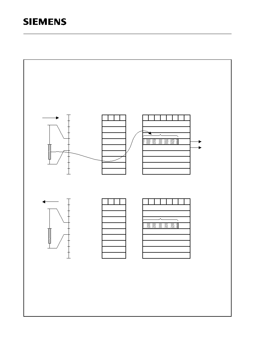
PEB 2055
PEF 2055
Application Hints
Semiconductor Group
184
After these programming steps, the EPIC memory will have the following contents:
Figure 67
Control Memory Contents for 6-Bit Signaling Channel Handling
ITD08082
1 0
Code Field
Data Field
Control Memory
CFI
Frame
0
127
Up-
stream
stream
Down-
127
0
P0, TS2
P0, TS3
0
0
1
0
1
P0, TS3
P0, TS2
0
1
1
1
1
1
1
0
0
1
X
X
X
X
X
X
X
1 1
X
SIG Value
1
1
1
1
0
1
0
0 0
1
1
0
SIG Value
1
Actual Value
Stable Value
1
0
1
1 1
1
1
1

PEB 2055
PEF 2055
Application Hints
Semiconductor Group
185
8-Bit Signaling Scheme
This option is intended for SLD channels where the even time slot consists of an 8 bit
feature control channel and the odd time slot of an 8 bit signaling channel.
The feature control channel is handled by the MF handler according to the selected
protocol, handshake or non-handshake. Note that only the non-handshake mode makes
sense in SLD applications.
The 8 bit SIG channel can be accessed by the
Ķ
P for controlling codec filter devices. In
upstream direction each valid change in the SIG value is reported by interrupt to the
Ķ
P
and the CFI time slot address is stored in the CIFIFO (refer to chapter 5.5.2). The
change detection mechanism consists of a double last look logic with a programmable
period.
To initialize two consecutive CFI time slots for the 8 bit signaling channel scheme, the
CM codes as given in table 31 must be used:
Example
In CFI mode 3, downstream time slots 2 and 3 and upstream time slots 6 and 7 of port
0 shall be initialized for 8 bit signaling channel handling:
W:MADR
=
0100 0101
B
; SIG value "0100 0101"
W:MAAR
=
0001 0000
B
; downstream even TS, port 0 time slot 2
W:MACR
=
0111 1011
B
; write CM code + data fields, CM code "1011"
W:MADR
=
XXXX XXXX
B
; don't care
W:MAAR
=
0001 0001
B
; downstream odd TS, port 0 time slot 3
W:MACR
=
0111 1011
B
; write CM code + data fields, CM code "1011"
W:MADR
=
1101 0110
B
; expected SIG value "1101 0110"
W:MAAR
=
1011 0000
B
; upstream even TS, port 0 time slot 6
W:MACR
=
0111 1011
B
; write CM code + data fields, CM code "1011"
W:MADR
=
1101 0110
B
; expected SIG value "1101 0110"
W:MAAR
=
1011 0001
B
; upstream odd TS, port 0 time slot 7
W:MACR
=
0111 1011
B
; write CM code + data fields, CM code "1011"
Table 31
CM Address
CM Code
CM Data
Even time slot downstream
Odd time slot downstream
Even time slot upstream
Odd time slot upstream
1010
1011
1011
1011
SIG
B
XXXXXXXX
B
actual value
B
stable value
B

PEB 2055
PEF 2055
Application Hints
Semiconductor Group
186
Summary of "Preprocessed Channel" Codes
Figure 68
Pre-processed Channel Codes
ITD09544
1
1
0
1
0
1
0
1
X X
X X
X
0 0 0 0
X X
X
C/I
1
1
1
0
0
0
1
1
1
1 0 0 0
1 1
1
C/I
X
X
0
1
0
1
1 0 1 1
Odd Time-Slot
Even Time-Slot
Upstream Preprocessed Channels
Input from the Configurable Interface
(e.g. SLD)
Signaling
8 Bit
6
(e.g. analog
Signaling
Bit
Handling
D Channel
Central
Handling
D Channel
Decentral
SIG Actual Value
SIG Actual Value
Value
Stable
SIG
Value
Stable
SIG
X X
: Monitor channel bits, these bits are treated by the monitor/feature control handler
m
- : Inactive sub. time-slot, in downstream direction these bits are tristated (OMDR : COS
or set to logical 1
C/I : Command/Indication channel, these bits are exchanged between the CFI in/output and the CM data field. A change of
the C/I bits in upstream direction causes an interrupt
: SFI). The address of the change is stored in the CIFIFO
D : D channel, these D channel bits are transparently switched to and from the PCM interface.
SIG : Signaling Channel, these bits are exchanged between the CFI in/output and the CM data field. The SIG value which
was present in the last frame is stored as the actual value in the even address CM location. The stable value is updated
if a valid change in the actual value has been detected according to the last look algorithm. A change of the SIG stable
value in upstream direction causes an interrupt (ISTA : CFI). The address of the change is stored in the CIFIFO.
actual value
stable value
(ISTA
= 0)
1)
=
COS
:
(OMDR
Decentral
D Channel
Handling
Central
D Channel
Handling
Bit
Signaling
(e.g. analog
R
)
IOM
6
Bit
8
Signaling
(e.g. SLD)
DD Application
Even Control Memory Address
MAAR = 0......0
Code Field
0111...
=
MACR
Data Field
......
=
MADR
0......1
=
MAAR
Odd Control Memory Address
Output at the Configurable Interface
Downstream Preprocessed Channels
Even Time-Slot
Odd Time-Slot
SIG
0
1
0
1
1 0 1 0
SIG
1 1
C/I
1
1
1
0
1
0
1
1
1
1 0 0 0
1 1
1
C/I
X
X
X
1
1
0
1
X
X
X
X
X
X X
X X
X
1 0 1 1
X X
X
X X
X X
X
1 0 1 1
X X
X
Pointer to a PCM Time-Slot
PCM Code for
a Bit Sub.
Time-Slot
C/I
m m
Monitor Channel
Control Channel
Control Channel
Monitor Channel
m
m
C/I
D D
SIG
m m
Monitor Channel
Control Channel
m m m m m m m m
SIG
Feature
Signaling Channel
Control Channel
- -
2
Code Field
MACR
......
= 0111...
Data Field
MADR =
m
m m
m
m m m m
m
m m
m
m m m m
m
m m
m
m m m m
Odd Control Memory Address
Code Field
MACR
Even Control Memory Address
MAAR
......
=
= 1......0
0111...
Data Field
MADR =
MAAR
Code Field
MACR
1......1
0111...
=
=
Data Field
MADR ......
=
Application
DD
IOM )
R
PCM Code for
Sub.
Bit
2
a
Time-Slot
Pointer to a PCM Time-Slot
Signaling Channel
Feature
Channel
Control
SIG
m
m m
m
m m m m
Monitor Channel
Control Channel
SIG
m m
m
m
m m
m m m m
m
m
m
m
m
m
m
m
m
m m
m
m m m m
Monitor Channel
Monitor Channel
Control Channel
Control Channel
-
-
C/I
m m
m
m
C/I
D
D

PEB 2055
PEF 2055
Application Hints
Semiconductor Group
187
5.5.2
Control/Signaling (CS) Handler
If the configurable interface (CFI) of the EPIC is operated as IOM or SLD interface, it is
necessary to communicate with the connected subscriber circuits such as layer-1
transceivers (ISDN line cards) or codec filter devices (analog line cards) over the
Command/Indication (C/I) or the signaling (SIG) channel. In order to simplify this task the
EPIC has implemented the Control/Signaling Handler (CS Handler).
In downstream direction, the 4, 6 or 8 bit C/I or SIG value can simply be written to the
Control Memory data field which will then be repeatedly transmitted in every frame to the
subscriber circuit until a new value is loaded.
Note that the downstream C/I or SIG value must always be written to the even CM
address in order to be transmitted in the subsequent odd CFI time slot!
In upstream direction a change detection mechanism is active to search for changes in
the received C/I or SIG values. Upon a change, the address of the involved subscriber
is stored in a 9 byte deep FIFO (CIFIFO) and an interrupt (ISTA:SFI) is generated. The
Ķ
P can then first determine the CM address by reading the FIFO before reading the new
C/I or SIG value out of the Control Memory. The address FIFO serves to increase the
latency time for the
Ķ
P to react to SFI interrupts. If several C/I or SIG changes occur
before the
Ķ
P executes the SFI interrupt handling routine, the addresses of the first
9 changes are stored in the CIFIFO and the corresponding C/I or SIG values are stored
in the control memory (CM). If more than 9 changes occur before the
Ķ
P reads the
CIFIFO, these additional changes are no longer updated in the control memory. This is
to prevent any loss of change information. These additional changes remain pending at
the serial interface. As soon as the
Ķ
P reads the CIFIFO, and thus, empties locations of
the FIFO, these pending changes are sequentially written to the CM and the
corresponding addresses to the FIFO. It is thus ensured that no change information is
lost even if, for example, all 32 subscribers simultaneously generate a change in their
C/I or SIG channel!
CFI time slots which should be processed by the CS handler must first be initialized as
MF/CS channels with appropriate codes in the Control Memory code field (refer to
chapter 5.5.1).

PEB 2055
PEF 2055
Application Hints
Semiconductor Group
188
5.5.2.1 Registers used in Conjunction with the CS Handler
In detail, the following register bits are used in conjunction with the CS handler:
Signaling FIFO
read
reset value:
0XXXXXXX
B
The 9 byte deep CIFIFO stores the addresses of CFI time slots in which a C/I and/or a
SIG value change has taken place. This address information can then be used to read
the actual C/I or SIG value from the Control Memory.
SBV:
Signaling Byte Valid; if SBV = 1, the SAD6 ... 0 bits indicate a valid
subscriber address. The polarity of SBV is chosen such that the
whole 8 bits of the CIFIFO can be copied to the MAAR register in
order to read the upstream C/I or SIG value from the Control Memory.
SAD6 ... 0:
Subscriber Address bits 6 ... 0; The CM address which corresponds
to the CFI time slot where a C/I or SIG value change has taken place
is encoded in these bits. For C/I channels SAD6 ... 0 point to an even
CM address (C/I value), for SIG channels SAD6 ... 0 point to an odd
CM address (stable SIG value).
Timer Register
write
reset value:
00
H
The EPIC timer can be used for 3 different purposes: timer interrupt generation
(ISTA:TIG), FSC multiframe generation (CMD2:FC2 ... 0 = 111), and last look period
generation.
In case of last look period generation, the following functions are provided:
SSR:
Signaling Sampling Rate; If SSR = 1, the last look period is fixed to
125
Ķ
s, i.e. the timer is not used at all for the last look logic. The value
programmed to TVAL has then no influence on the last look period.
The timer can then still be used for timer interrupt generation, and/or
FSC multiframe generation, with a period as defined by TVAL6 ... 0.
If SSR = 0, the last look period is defined by TVAL6 ... 0. Note that if
the timer is used, it must also be started with CMDR:ST = 1.
bit 7
bit 0
CIFIFO
SBV
SAD6
SAD5
SAD4
SAD3
SAD2
SAD1
SAD0
bit 7
bit 0
TIMR
SSR
TVAL6
TVAL5
TVAL4
TVAL3
TVAL2
TVAL1
TVAL0

PEB 2055
PEF 2055
Application Hints
Semiconductor Group
189
TVAL6 ... 0:
Timer Value bits 6 ... 0; the timer period, equal to
(1 + TVAL6 ... 0)
◊
250
Ķ
s, is programmed here. It can thus be
adjusted within the range of 250
Ķ
s up to 32 ms.
The timer is started as soon as CMDR:ST is set to 1 and stopped by writing the TIMR
register or by selecting OMDR:OMS0 = 0.
If the timer is used to generate the last look period, it can still be used for timer interrupt
generation and/or FSC multiframe generation if it is acceptable that all three applications
use the same timer value.
Command Register
write
reset value:
00
H
Writing a logical 1 to a CMDR register bit starts the respective operation.
The signaling handler uses two command bits:
ST:
Start Timer; must be set to 1 if the last look period is defined by
TIMR:TVAL6 ... 0, i.e. if TIMR:SSR = 0. Note that if TIMR:SSR = 1,
the timer need not be started.
CFR:
CIFIFO Reset; setting CFR to logical 1 resets the signaling FIFO
within 2 RCL periods, i.e. all entries and the ISTA:SFI bit are cleared.
Status Register
read
reset value:
05
H
The status register STAR displays the current state of certain events within the EPIC.
The STAR register bits do not generate interrupts and are not modified by reading
STAR.
The following bit is indirectly used by the signaling handler:
TAC:
Timer Active; the timer is running if TAC is set to logical 1, the timer
is not running if TAC is set to logical 0.
Note:The timer is only necessary for signaling channels (not C/I) and
when using a last look period greater or equal to 250
Ķ
s.
bit 7
bit 0
CMDR
0
ST
TIG
CFR
MFT1
MFT0
MFSO
MFFR
bit 7
bit 0
STAR
MAC
TAC
PSS
MFTO
MFAB
MFAE
MFRW
MFFE

PEB 2055
PEF 2055
Application Hints
Semiconductor Group
190
Interrupt Status Register
read
reset value:
00
H
The ISTA register should be read after an interrupt in order to determine the interrupt
source.
In connection with the signaling handler one maskable (MASK) interrupt bit is provided
by the EPIC in the ISTA register:
SFI:
Signaling FIFO Interrupt; This bit is set to logical 1 if there is at least
one valid entry in the CIFIFO indicating a change in a C/I or SIG
channel. Reading ISTA does not clear the SFI bit. Instead SFI is
cleared (logical 0) if the CIFIFO is empty which can be accomplished
by reading all valid entries of the CIFIFO or by resetting the CIFIFO
by setting CMDR:CFR to 1.
Note:The MASK:SFI bit only disables the interrupt pin (INT); the
ISTA:SFI bit will still be set to logical 1.
5.5.2.2 Access to Downstream C/I and SIG Channels
If two consecutive downstream CFI time slots, starting with an even time slot number,
are programmed as MF and CS channels, the
Ķ
P can write a 4, 6 or 8 bit wide C/I or SIG
value to the even addressed downstream CM data field. This value will then be
transmitted repeatedly in the odd CFI time slot until a new value is loaded.
This value, first written into MADR, can be transferred to the CM data field using the
memory operation codes MACR:MOC = 111X or MACR:MOC = 1001 (refer to
chapter 5.3.3.3).
The code MACR:MOC = 111X applies if the code field has not yet been initialized with
a CS channel code. Writing to MACR with MACR:RWS = 0 will then copy the CS channel
code written to MACR:CMC3 ... CMC0 to the CM code field and the value written to
MADR to the CM data field. The CM address (CFI time slot) is specified by MAAR
according to figure 48.
The code MACR:MOC = 1001 applies if the code field has already been properly
initialized with a CS channel code. In this case only the MADR content will be copied to
the CM data field addressed by MAAR.
bit 7
bit 0
ISTA
TIN
SFI
MFFI
MAC
PFI
PIM
SIN
SOV

PEB 2055
PEF 2055
Application Hints
Semiconductor Group
191
The value written to MADR should have the following format:
4 bit C/I value: MADR = 1 1 _ _ _ _ 1 1
B
6 bit SIG value: MADR = _ _ _ _ _ _ 1 1
B
8 bit SIG value: MADR = _ _ _ _ _ _ _ _
B
Examples
In CFI mode 0 the downstream time slots 6 and 7 of port 2 shall be initialized as MF and
CS channels, 6 bit signaling scheme. The initialization value shall be `010101':
W:MADR
=
0101 0111
B
; SIG value `010101'
W:MAAR
=
0001 1100
B
; downstream, port 2, time slot 6
W:MACR
=
0111 1010
B
; write CM code + data fields, CM code `1010'
W:MADR
=
XXXX XXXX
B
; don't care
W:MAAR
=
0001 1101
B
; downstream, port 2, time slot 7
W:MACR
=
0111 1011
B
; write CM code + data fields, CM code `1011'
The above programming sequence can for example be performed during the
initialization phase of the EPIC. Once the CFI time slots have been loaded with the
appropriate codes ('1010' in time slot 6 and `1011' in time slot 7), an access to the
downstream SIG channel (time slot 7) can be accomplished simply by writing a new
value to the address of time slot 6:
W:MADR
=
1100 1111
B
; new SIG value `110011'
W:MAAR
=
0001 1100
B
; downstream, port 2, time slot 6
W:MACR
=
0100 1000
B
; write CM DF, MOC = 1001
5.5.2.3 Access to the Upstream C/I and SIG Channels
If two consecutive upstream CFI time slots, starting with an even time slot number, are
programmed as MF and CS channels, the
Ķ
P can read the received 4, 6 or 8 bit C/I or
SIG values simply by reading the upstream CM data field.
Two cases can be distinguished:
When a 4 bit Command/Indication handling scheme is selected, the C/I value received
in the odd CFI time slot can be read from the even CM address. This value is sampled
in each frame (every 125
Ķ
s). Each change is furthermore indicated by an ISTA:SFI
interrupt and the address of the corresponding even CM location is stored in the CIFIFO.
Since the MSB of the CIFIFO is set to 1 for a valid entry (SBV = 1), the value read from
the CIFIFO can directly be copied to MAAR in order to read the upstream CM data field
which also requires an MSB set to 1 (U/D = 1).
When a 6 or 8 bit signaling scheme is selected, the received SIG value is sampled at
intervals of 125
Ķ
s or (TVAL + 1)
◊
250
Ķ
s and stored as the "actual value" at the even
CM address. The
Ķ
P can access the actual value simply by reading this even CM data
field location. Additionally, a "stable value", based on the double last look algorithm is
generated: in order to assure that erroneous bit changes at the sampling time point do

PEB 2055
PEF 2055
Application Hints
Semiconductor Group
192
not initiate a definite change, the values of two consecutive sampling points are
compared with the current old stable value. The stable value is then only updated if both
new values are identical and differ from the old stored value. The stable value can be
read from the odd CM data field location. Each change in the stable value is furthermore
indicated by an ISTA:SFI interrupt and the address of the corresponding odd CM
location is stored in the CIFIFO. Since the MSB of the CIFIFO is set to 1 for a valid entry
(SBV = 1), the value read from the CIFIFO can directly be copied to MAAR in order to
read the upstream CM data field, which also requires an MSB set to 1 (U/D = 1).
Note: The sampling interval is selected in the TIMR register (refer to chapter 5.5.2.1).
If the sampling interval is set to 125
Ķ
s (TIMR:SSR = 1), it is not necessary to start
the timer to operate the change detection logic. If, however, the last look period is
determined by TIMR:TVAL6 ... 0 (TIMR:SSR = 0) it is required to start the timer
(CMDR:ST = 1) to operate the change detection logic and to generate SFI
interrupts.
Examples
In CFI mode 0 the upstream time slots 6 and 7 of port 2 shall be initialized as MF and
CS channels, 6 bit signaling scheme, the expected value from the codec after power up
shall be "011101":
W:MADR
=
0111 0111
B
; expected actual value "011101"
W:MAAR
=
1001 1100
B
; upstream, port 2, time slot 6
W:MACR
=
0111 1010
B
; write CM code + data fields, CM code "1010"
W:MADR
=
0111 0111
B
; expected stable value "011101"
W:MAAR
=
1001 1101
B
; upstream, port 2, time slot 7
W:MACR
=
0111 1010
B
; write CM code + data fields, CM code "1010"
The above programming sequence can for example be performed during the
initialization phase of the EPIC. At this stage the CFI is not operational (OMDR = 80
H
),
i.e. the values received at the CFI are ignored.

PEB 2055
PEF 2055
Application Hints
Semiconductor Group
193
If the expected value "011101" is actually received upon activation of the CFI (e.g.
OMDR = EE
H
), no interrupt will be generated at this moment. But the change detection
is now enabled and each valid change in the received SIG value (e.g. new value
"001100") will generate an interrupt, with the address being stored in the CIFIFO. The
reaction of the
Ķ
P to such an event would then look like this:
R:ISTA
=
0100 0000
B
; SFI interrupt
R:CIFIFO
=
1001 1101
B
; address of upstream, port 2, time slot 7
W:MAAR =
1001
1101
B
; copy the address from CIFIFO to MAAR
W:MACR
=
1100 1000
B
; read back command for CM DF, MOC = 1001
wait for STAR:MAC = 0
R:MADR
=
0011 00XX
B
; read new SIG value (e.g. 001100)
wait for further ISTA:SFI interrupts
5.5.3
Monitor/Feature Control (MF) Handler
If the configurable interface CFI of the EPIC is configured as IOM or SLD interface, it is
necessary to communicate with the connected subscriber circuits such as layer-1
transceivers (ISDN line cards) or codec filter devices (analog line cards) over the monitor
channel (IOM) or feature control channel (SLD). In order to simplify this task the EPIC
has implemented the Monitor/Feature Control (MF) Handler which autonomously
controls and supervises the data transfer via these channels.
The communication protocol used in an MF channel is interface and subscriber circuit
specific.
Three cases can be distinguished:
IOM
ģ
-2 Interface Protocol
In this case the monitor channel protocol is a handshake procedure used for high speed
information exchange between the EPIC and other devices such as the IEC-Q
(PEB 2091), SBCX (PEB 2081) or SICOFI2 (PEB 2260).
The monitor channel operates on an asynchronous basis. While data transfers on the
IOM
-
2 interface take place synchronized to the IOM frame, the flow of data is controlled
by a handshake procedure based on the monitor channel receive (MR) and the monitor
channel transmit (MX) bits located at the end of the fourth time slot of the respective
IOM
-
2 channel.
For the transmission of a data byte for example, the data is placed onto the downstream
monitor channel and the MX bit is activated. This byte will then be transmitted repeatedly
once per 8 kHz frame until the receiver acknowledges the transfer via the upstream MR
bit.
A detailed description of the IOM-2 monitor channel operation can be found in the
"IOM-2 Interface Reference Guide".

PEB 2055
PEF 2055
Application Hints
Semiconductor Group
194
IOM
ģ
-1 Interface Protocol
In this case the monitor channel protocol is a non handshake procedure which can be
used to exchange one byte of information at a time between the EPIC and a layer-1
device such as the IBC (PEB 2095) or the IEC-T (PEB 2090).
Data bytes to be transmitted are sent once in the downstream monitor channel. Since
the monitor channel is idle (FF
H
) when no data is being transmitted, the receiving device
accepts only valid data bytes which are different from FF
H
. If a message shall be sent
back to the EPIC, this must occur in the frame following the frame of reception.
SLD Interface Protocol
The transfer of control information over the feature control channel of an SLD interface
e.g. for programming the coefficients to a SICOFI (PEB 2060) device is also performed
without a handshake procedure. Data is transmitted and received synchronous to the
8 kHz frame at a speed of one data byte per frame.
The MF handler of the EPIC supports all three kinds of protocols. A bidirectional 16 byte
FIFO, the MFFIFO, serves as data buffer for outgoing and incoming MF messages in all
protocol modes. This implies that the MF communication is always performed on a
half-duplex basis.
Differentiation between IOM-2 and IOM-1/SLD modes is made via the MF Protocol
Selection bit MFPS in the Operation Mode Register OMDR.
Since the IOM-1 and SLD protocols are very similar, they are treated by the EPIC in
exactly the same way i.e. without handshake protocol. The only processing difference
concerns the involved upstream time slot when receiving data:
When configured as IOM interface (CFI modes 0, 1 or 2), the CFI ports consist of
separate upstream (DU) and downstream (DD) lines. In this case MF data is transmitted
on DD and received on DU of the same CFI time slot.
When configured as SLD interface (CFI mode 3), the CFI ports consist of bidirectional
lines (SIP). The first four time slots of the frame are used as downstream time slots and
the last four as upstream time slots. In this case the MF data is transmitted in the
downstream feature control time slot and received on the same CFI line but four time
slots later in the upstream feature control time slot.
CFI time slots which should be processed by the MF handler must first be initialized as
MF/CS channels with appropriate codes in the Control Memory Code Field (refer to
chapter 5.5.1).
Except for broadcast operation, communication over the MF channel is only possible
with one subscriber circuit at a time. The MF handler must therefore be pointed to that
particular time slot via the address register MFSAR.
Normally MF channel transfers are initiated by the EPIC (master). The subscriber circuits
(slaves) will only send back monitor messages upon a request from the master device.

PEB 2055
PEF 2055
Application Hints
Semiconductor Group
195
In IOM-2 applications, however, (active handshake protocol), it is also possible that a
slave device requests a data transfer e.g. when an IEC-Q device has received an EOC
message over the U interface.
For these applications the EPIC has implemented a search mechanism that looks for
active handshake bits. When such a monitor channel is found, the
Ķ
P is interrupted
(ISTA:MAC) and the address of the involved MF channel is stored in a register (MFAIR).
The MF handler can then be pointed to that channel by copying the contents of MFAIR
to MFSAR and the actual message transfer can take place.
5.5.3.1 Registers used in Conjunction with the MF Handler
In detail, the following registers are involved when performing MF channel transfers:
Operation Mode Register
read/write
reset value:
00
H
MFPS:
MF channel Protocol Selection;
MFPS = 0: Handshake facility disabled; to be used for SLD and
IOM-1 applications.
MFPS = 1: Handshake facility enabled; to be used for IOM-2
applications.
Monitor/Feature Control Channel FIFO
read/write reset value:
empty
The 16 byte bidirectional MFFIFO provides intermediate storage for data bytes to be
transmitted or received over the monitor or feature control channel.
Note: The data transfer over an MF channel is half-duplex i.e. if a "transmit + receive"
command is issued, the transmit section of the transfer must first be completed
before the receive section starts.
MFD7 ... 0:
MF Data bits 7 ... 0; MFD7 (MSB) is the first bit to be sent over the
serial CFI, MFD0 (LSB) the last.
bit 7
bit 0
OMDR:
OMS1
OMS0
PSB
PTL
COS
MFPS
CSB
RBS
bit 7
bit 0
MFFIFO:
MFD7
MFD6
MFD5
MFD4
MFD3
MFD2
MFD1
MFD0
PEB 2055
PEF 2055
Application Hints
Semiconductor Group
196
MF Channel Subscriber Address Register
write reset value:
undefined
The exchange of monitor data normally takes place with only one subscriber circuit at a
time. This register serves to point the MF handler to that particular CFI time slot.
MFTC1 ... 0:
MF Channel Transfer Control 1 ... 0; these bits, in addition to
CMDR:MFT1,0 and OMDR:MFPS control the MF channel transfer as
indicated in table 32.
SAD5 ... 0:
Subscriber address 5 ... 0; these bits define the addressed
subscriber. The CFI time slot encoding is similar to the one used for
Control Memory accesses using the MAAR register (see figure 48).
CFI time slot encoding of MFSAR derived from MAAR:
MAAR:MA7 selects between upstream and downstream CM blocks. This information is
not required since the transfer direction is defined by CMDR (transmit or receive).
MAAR:MA0 selects between even and odd time slots. This information is also not
required since MF channels are always located on even time slots.
bit 7
bit 0
MFSAR:
MFTC1
MFTC0
SAD5
SAD4
SAD3
SAD2
SAD1
SAD0
MAAR:
MA7
MA6
MA5
MA4
MA3
MA2
MA1
MA0
MFSAR: MFTC1 MFTC0 SAD5
SAD4
SAD3
SAD2
SAD1
SAD0

PEB 2055
PEF 2055
Application Hints
Semiconductor Group
197
Example
In CFI mode 0, IOM channel 5 (time slot 16 ... 19) of port 2 shall be addressed for a
transmit monitor transfer:
MFSAR = 0010 0110
B
; the monitor channel occupies time slot 18 (10010
B
) of port 2
(10
B
)
MF Channel Active Indication Register
read
reset value:
undefined
This register is only used in IOM-2 applications (active handshake protocol) in order to
identify active monitor channels when the `Search for active monitor channels' command
(CMDR:MFSO) has been executed.
SO:
MF Channel Search On; this bit indicates whether the EPIC is still
busy looking for an active channel (1) or not (0).
SAD5 ... 0:
Subscriber Address 5 ... 0; after an ISTA:MAC interrupt these bits
point to the port and time slot where an active channel has been
found. The coding is identical to MFSAR:SAD5 ... SAD0. The
contents of MFAIR can directly be copied to MFSAR in order to point
the MF handler to the channel which requests a monitor receive
operation.
Command Register
read
reset value:
00
H
Writing to CMDR starts the respective monitor channel operation.
MFT1 ... 0:
MF Channel Transfer Control Bits 1, 0; these bits start the monitor
transfer enabling the contents of the MFFIFO to be exchanged with
the subscriber circuits as specified in MFSAR. The function of some
commands depends furthermore on the selected protocol
(OMDR:MFPS).
Table
32 summarizes all available MF commands.
MFSO:
MF Channel Search On; if set to 1, the EPIC starts to search for active
MF channels. Active channels are characterized by an active MX bit
(logical 0) sent by the remote transmitter. If such a channel is found,
bit 7
bit 0
MFAIR:
0
SO
SAD5
SAD4
SAD3
SAD2
SAD1
SAD0
bit 7
bit 0
CMDR
0
ST
TIG
CFR
MFT1
MFT0
MFSO
MFFR

PEB 2055
PEF 2055
Application Hints
Semiconductor Group
198
the corresponding address is stored in MFAIR and an ISTA:MAC
interrupt is generated. The search is stopped when an active MF
channel has been found or when OMDR:OMS0 is set to 0.
MFFR:
MFFIFO Reset; setting this bit resets the MFFIFO and all operations
associated with the MF handler (except for the search function) within
2 RCL periods. The MFFIFO is set into the state `MFFIFO empty,
write access enabled' and any monitor data transfer currently in
process will be aborted. MFFR should be set when all data bytes have
been read from the MFFIFO after a monitor receive operation.
1)
Handshake facility disabled (OMDR:MFPS = 0)
2)
Handshake facility enabled (OMDR:MFPS = 1)
Table 32
Transfer Mode
CMDR:
MFT, MFT0
MFSAR
Protocol
Selection
Application
Inactive
00
XXXXXXXX
HS, no HS
1)
idle state
Transmit
01
00 SAD5 ... 0
HS, no HS
1)
IOM-2, IOM-1, SLD
Transmit
Broadcast
01
01XXXXXX
HS, no HS
1)
IOM-2, IOM-1, SLD
Test Operation
01
10 - - - - - -
HS, no HS
1)
IOM-2, IOM-1, SLD
Transmit
Continuous
11
00 SAD5 ... 0
HS
2)
IOM-2
Transmit + Receive
Same Time Slot
Any # of Bytes
1 byte expected
2 bytes expected
8 bytes expected
16 bytes expected
10
10
10
10
10
00 SAD5 ... 0
00 SAD5 ... 0
01 SAD5 ... 0
10 SAD5 ... 0
11 SAD5 ... 0
HS
2)
no HS
1)
no HS
1)
no HS
1)
no HS
1)
IOM-2
IOM-1
(IOM-1)
(IOM-1)
(IOM-1)
Transmit + Receive
Same Line
1 byte expected
2 bytes expected
8 bytes expected
16 bytes expected
11
11
11
11
00 SAD5 ... 0
01 SAD5 ... 0
10 SAD5 ... 0
11 SAD5 ... 0
no HS
1)
no HS
1)
no HS
1)
no HS
1)
SLD
SLD
SLD
SLD

PEB 2055
PEF 2055
Application Hints
Semiconductor Group
199
Status Register
read
reset value:
00
H
The status register STAR displays the current state of the MFFIFO and of the monitor
transfer operation. It should be interrogated after an ISTA:MFFI interrupt and prior to
accessing the MFFIFO.
The STAR register bits do not generate interrupts and are not modified by reading
STAR.
MFTO:
MF Channel Transfer in Operation; an MF channel transfer is in
operation (1) or not (0).
MFAB:
MF Channel Transfer Aborted; a logical 1 indicates that the remote
receiver aborted a handshaked message transfer.
MFAE:
MFFIFO Access Enable; the MFFIFO may be either read or written to
(1) or it may not be accessed (0).
MFRW:
MFFIFO Read/Write; if MFAE is set to logical 1 the MFFIFO may be
read (1) or is ready to be written to (0).
MFFE:
MFFIFO Empty; the MFFIFO is empty (1) or not empty (1).
Interrupt Status Register
read
reset value:
00
H
The ISTA register should be read after an interrupt in order to determine the interrupt
source. In connection with the monitor handler two maskable (MASK) interrupt bits are
provided by the EPIC:
MFFI:
MFFIFO interrupt; if this bit is set to 1, the last MF channel command
(issued by CMDR:MFT1, MFT0) has been executed and the EPIC is
ready to accept the next command. Additional information can be
read from STAR:MFTO ... MFFE. MFFI is reset by reading ISTA.
MAC:
Monitor Channel Active Interrupt; this bit set to 1 indicates that the
EPIC has found an active monitor channel. A new search can be
started by reissuing the CMDR:MFSO command. MAC is reset by
reading ISTA.
bit 7
bit 0
STAR
MAC
TAC
PSS
MFTO
MFAB
MFAE
MFRW
MFFE
bit 7
bit 0
ISTA
TIN
SFI
MFFI
MAC
PFI
PIM
SIN
SOV

PEB 2055
PEF 2055
Application Hints
Semiconductor Group
200
5.5.3.2 Description of the MF Channel Commands
Transmit Command
The transmit command can be used for sending MF data to a single subscriber circuit
when no answer is expected. It is applicable for both handshake and non handshake
protocols. The message (up to 16 bytes) can be written to the MFFIFO after interrogation
of the STAR register. After writing of the MF channel address to MFSAR the transfer can
be started using the transmit command (CMDR = 04
H
). The contents of the MFFIFO will
then be transmitted byte by byte to the subscriber circuit.
If the handshake facility is disabled (IOM-1/SLD), the data is sent at a speed of one byte
per frame.
If the handshake facility is enabled (IOM-2), each data byte must be acknowledged by
the subscriber circuit before the next one is sent. The transfer speed depends therefore
on the reaction time of the subscriber circuit. The EPIC can transmit a message at a
maximum speed of one byte per two frames.
In order to avoid blocking the software when a subscriber circuit fails to acknowledge a
message, a software time out, which resets the monitor transfer (CMDR = 01
H
) should
be implemented.
If the remote partner aborts the reception of an arriving message i.e. if the EPIC detects
an inactive MR bit during at least two consecutive frames, the transmit operation will be
stopped, the ISTA:MFFI interrupt will be generated and the STAR:MFAB bit will be set
to 1. The CMDR:MFFR bit should then be set to clear the MFAB bit before the next
transfer.
When all data bytes of the MFFIFO have been sent (and eventually acknowledged) the
EPIC generates an ISTA:MFFI interrupt indicating the end of the transfer. The MF
handler may then be pointed to another subscriber address for another monitor transfer.

PEB 2055
PEF 2055
Application Hints
Semiconductor Group
201
Figure 69
Flow Diagram "Transmit Command"
Transmit Continuous Command
The transmit continuous command can be used in IOM-2 applications only (active
handshake protocol) to send monitor messages longer than 16 bytes to a single
subscriber circuit.
When this command is given, the EPIC transmits the contents of the MFFIFO as with the
normal transmit command but does not conclude the transfer by setting MX inactive
when the MFFIFO is empty. Instead, the
Ķ
P is interrupted (ISTA:MFFI) and requested to
write a new block of data into the MFFIFO. This block may then again be transmitted
using the transmit continuous command or, if it is the last block of the long message, it
may be transmitted using the normal transmit command (CMDR:MFT1, MFT0 = 01). If
an answer is expected from the subscriber circuit, the last block may also be terminated
using the transmit + receive command (CMDR:MFT1, MFT0 = 10). Each message block
may be of arbitrary length (1 to 16 bytes).
ITD08085
R
EPIC
P
Ķ
W : CMDR = 01
MFFR
MFFIFO Reset
R : STAR = 05
MFAE, MFFE
MFFIFO Empty
Write Access Enabled
1
2
N
Write Access Enabled
MFFIFO not Empty
MFT1, 0 = 01
MFTC1, 0 = 00
MFFIFO not Empty
Access Disabled
Transfer in Operation
MFTO, MFRW, MFFE
MFFIFO Empty
Transfer in Operation
Access Disabled
MFFI Interrupt
MFFIFO Empty
Write Access Enabled
Transfer Completed
MR = 0
MR = 1
Da 1
Ack 1
Da 2
Ack 2
Da N
Ack N
W : MFFIFO = Data
W : CMDR = 04
W : MFSAR = Address
R : STAR = 04
R : STAR = 12
R : STAR = 13
R : ISTA = 20
R : STAR = 05

PEB 2055
PEF 2055
Application Hints
Semiconductor Group
202
Figure 70
Flow Diagram "Transmit Continuous Command"
Transmit + Receive Same Time Slot Command
The transmit + receive same time slot command can be used to send a message to a
subscriber circuit, which will respond with an answer, e.g. reading back the coefficients
of a SICOFI device. After first transmitting the contents of the MFFIFO (as with the
normal transmit command), the MFFIFO is ready to accept an incoming message which
can then be read by the
Ķ
P when the transfer is completed.
ITD08086
W : CMDR = 01
R : STAR = 05
MFFIFO Reset
MFFIFO Empty
Write Access Enabled
1
2
16
MFAE,
MFFR
MFFE
MFTC1, 0 = 00
MFT1, 0 = 11
MFFIFO not Empty
Write Access Enabled
MFFIFO not Empty
Access Disabled
Transmit Transfer
in Operation
MFFI Interrupt
MFFIFO Empty
Write Access Enabled
Transfer in Operation
17
18
N
MFFIFO not Empty
Write Access Enabled
Transfer in Operation
MFT1, 0 = 01
Transmit Transfer
Access Disabled
MFFIFO not Empty
MFTO, MFRW, MFFE
in Operation
MFFIFO Empty
Access Disabled
Transfer in Operation
MFFI Interrupt
MFFIFO Empty
Write Access Enabled
Transfer Completed
MR = 1
MR = 0
Ack N
Da N
Ack 18
Da 18
Ack 17
Da 17
MX = 0
MX = 0
Da 1
Ack 1
Da 2
Ack 2
Da 16
Ack 16
Ķ P
EPIC
R
W : MFFIFO = Data
W : CMDR = 0C
W : MFSAR = Address
W : MFFIFO = Data
W : CMDR = 04
R : STAR = 04
R : STAR = 12
R : ISTA = 20
R : STAR = 15
R : STAR = 14
R : STAR = 12
R : STAR = 13
R : ISTA = 20
R : STAR = 05

PEB 2055
PEF 2055
Application Hints
Semiconductor Group
203
This command can also be used to perform a receive only operation: if a message shall
be received without transmission (e.g. after an active monitor channel has been found)
the transmit + receive command is issued with an empty MFFIFO.
The command is applicable for both handshake and non-handshake protocols. Since the
transfer operation is performed on the same time slot, its use is intended for IOM
applications:
≠ IOM-2, handshake facility enabled:
The contents of the MFFIFO is sent to the subscriber circuit subject to the IOM-2 protocol
i.e each byte must be acknowledged before the next one is sent. When the MFFIFO is
empty, the EPIC starts to receive the incoming data bytes, each byte being
autonomously acknowledged by the EPIC. Up to 16 bytes may be stored in the MFFIFO.
When the end of message is detected (MX bit inactive during two consecutive frames),
the transfer is considered terminated and an ISTA:MFFI interrupt is generated. The
Ķ
P
can then fetch the message from the MFFIFO. In order to determine the length of the
arrived message, the STAR:MFFE bit (MFFIFO Empty) should be evaluated before each
read access to the MFFIFO. After all bytes have been read, the MFFIFO must be reset
with the CMDR:MFFR command in order to enable new monitor transfer operations.

PEB 2055
PEF 2055
Application Hints
Semiconductor Group
204
Figure 71
Flow Diagram "Transmit + Receive Same Time Slot Command"
The reception of monitor messages may also (if required) be aborted at any time simply
by setting the CMDR:MFFR bit while the receive transfer is still in operation.
If more than 16 bytes shall be received, the following procedure can be adopted:
The first 16 data bytes received will be stored in the MFFIFO and acknowledged to the
remote partner. The presence of a 17
th
byte on the receive line will lead to an ISTA:MFFI
interrupt. While the transfer is still in operation (STAR = 16
H
), with the 17
th
byte still left
unacknowledged, the
Ķ
P can read the first 16 bytes out of the MFFIFO. When this is
ITD08087
W : CMDR = 01
R : STAR = 05
MFFIFO Reset
MFFIFO Empty
Write Access Enabled
1
2
N
MFAE,
MFFR
MFFE
MFTC1, 0 = 00
MFT1, 0 = 10
MFFIFO not Empty
Write Access Enabled
MFFIFO not Empty
Access Disabled
Transmit Transfer
in Operation
MFFIFO Empty
Access Disabled
Transfer in Operation
Receive Transfer
Access Disabled
MFFIFO not Empty
MFAE, MFRW, MFFE
in Operation
MFFIFO not Empty
Read Access Enabled
Transfer Completed
MFFI Interrupt
MFFIFO Empty
Read Access Enabled
Ack
Da
Ack
Da
Ack
Da
M
2
1
M
2
1
MR = 1
1
2
N
1
2
N
Da
Ack
Da
Ack
Da
Ack
MFTO, MFRW,MFFE
MFFE
No Transfer in Operation
Access Disabled
MFFIFO Empty
MFTO
1
2
M
0
=
MR
R
EPIC
P
Ķ
W : MFFIFO = Data
W : MFSAR = Address
W : CMDR = 08
R : STAR = 04
R : STAR = 12
R : STAR = 13
R : STAR = 01
R : STAR = 10
R : ISTA = 20
R : STAR = 06
R : MFFIFO = Data
R : STAR = 07

PEB 2055
PEF 2055
Application Hints
Semiconductor Group
205
done (STAR = 17
H
), the
Ķ
P issues again (with an empty MFFIFO) the transmit + receive
command (CMDR = 08
H
) and the EPIC is again ready to receive and acknowledge
further monitor bytes.
≠ IOM-1, handshake facility disabled
The contents of the MFFIFO are sent to the subscriber circuit at a speed of 1 byte per
frame. When the last byte has been transmitted, the EPIC stores the received monitor
bytes of the next subsequent frames into the MFFIFO. The receive transfer is completed
and an ISTA:MFFI interrupt is generated after either 1, 2, 8, or 16 frames. The actual
number of stored bytes can be selected with MFSAR:MFTC1,MFTC0.
Transmit + Receive Same Line Command
This command is similar to the Transmit + Receive same time slot command i.e. it can
be used to send a message to a subscriber circuit which will respond with an answer. Its
use is, however, intended for SLD applications: CFI mode 3, 8 time slots/frame,
handshake facility disabled.
The transmit operation is performed in the downstream time slot specified in MFSAR
while the receive operation is performed on the same SIP line, but four time slots later
in the upstream time slot.
Transmit Broadcast Command
The Transmit Broadcast Command can be used for sending a monitor/feature control
message to all subscriber circuits simultaneously. It is applicable for both handshake
and non handshake protocols. The procedure is similar to the normal transmit command
with the exception that the contents of the MFFIFO is transmitted on all downstream MF
time slots (defined by the CM code field). If the handshake protocols is active (IOM-2)
the data bytes are transmitted at a speed of one byte per three frames and the arriving
acknowledgments are ignored.
Test Operation Command
When executing the Test Operation Command, a message written to the MFFIFO will
not be transmitted to the subscriber circuit but may instantaneously be read back. All
interrupts (ISTA) and status (STAR) bits will be generated in the same manner as for a
normal transmit + receive transfers. It is applicable for both handshake and
non-handshake protocols.

PEB 2055
PEF 2055
Application Hints
Semiconductor Group
206
Search For Active Monitor Channels Command
In IOM-2 applications the monitor channel is sometimes used for low speed data
transfers over the S and Q channels of an S interface or over the EOC channel of a U
(2B1Q) interface. The layer-1 transceivers (SBCX PEB 2081, IEC-Q PEB 2091) may
then, upon reception of a new message, start a monitor channel communication with the
EPIC.
For those applications where a slave device initiates an MF channel transfer, the EPIC
has implemented the "Search For Active Monitor Channels Command".
The active handshake protocol (OMDR:MFPS = 1) must be selected for this function.
When the "MF Search On" command (CMDR:MFSO = 1) is executed, the EPIC
searches for active handshake bits (MX) on all upstream monitor channels. As soon as
an active channel is found, an ISTA:MAC interrupt is generated, the search is stopped,
and the address of this channel is stored in MFAIR. The
Ķ
P can then copy the value of
MFAIR to MFSAR in order to point the MF handler to that particular channel. With an
empty MFFIFO the transmit + receive same time slot command can be executed to
initiate the reception of the monitor message. The EPIC will then autonomously
acknowledge each received byte and report the end of the transfer by an ISTA:MFFI
interrupt. The
Ķ
P can read the message from the MFFIFO and, if required, execute a
new MF Search command.
Note: The search should only be started when no receive transfer is in operation,
otherwise each received byte will lead to the ISTA:MAC interrupt.
Once started, the search for active monitor channels can only be stopped when such a
channel has been found or when the Control Memory is reset or initialized
(OMDR:OMS0 = 0).

PEB 2055
PEF 2055
Application Hints
Semiconductor Group
207
Figure 72
Flow Diagram "Search For Active Monitor Channels Command"
ITD08088
W : CMDR = 02
MFSO
Search for Active
R : MFAIR = 01XXXXXX
Write Access Enabled
MFFIFO Empty
MFT1, 0 = 10
MFFIFO Empty
Access Disabled
Receive Transfer
MFFIFO not Empty
Transfer Completed
Read Access Enabled
MFFI Interrupt
Ack 1
Da 2
Ack 2
Da M
Ack M
Monitor Channels is On
MAC Interrupt
Channel Found
Search is Off
in Operation
1
2
M
MFAE, MFRW, MFFE
MFFIFO Empty
Read Access Enabled
Da 1
R
EPIC
P
Ķ
W : MFSAR = MFAIR
W : CMDR = 08
W : MFFIFO = Data
R : ISTA = 10
R : MFAIR = 00 SAD5...0
R : STAR = 05
R : STAR = 10
R : ISTA = 20
R : STAR = 06
R : STAR = 07

PEB 2055
PEF 2055
Application Hints
Semiconductor Group
208
5.6
Ķ
P Channels
If a CFI time slot shall be accessed by the
Ķ
P instead of being switched to the PCM
interface, this channel can be configured as a
Ķ
P channel. This is achieved by writing
the code `1001' to the CM code field. In this case the content of the corresponding CFI
time slot is directly exchanged with the CM data field. Figure 73 and figure 74 illustrate
the use of the Control Memory (CM) data and code fields for such applications.
If a CFI time slot is initialized as
Ķ
P channel, the function taken on by the CM data field
can be compared to the function taken on by the Data Memory (DM) data field at the
PCM interface, i.e. it buffers the PCM data received or to be transmitted at the serial
interface. In contrast to the PCM interface, where PCM idle channels can be
programmed on a 2 bit subtime slot basis, the CFI only allows
Ķ
P access for full 8 bit
time slots.
Figure 73
Ķ
P Access to the Downstream CFI Frame
ITD08089
.
.
MA6
0
MACR:
Data Field
Control Memory
MADR:
MAAR:
Code Field
stream
Down-
127
0
CFI
Frame
.
.
. MA0
0
1 0 0
1 0 0 0
1
0
0
1

PEB 2055
PEF 2055
Application Hints
Semiconductor Group
209
Figure 74
Ķ
P Access to the Upstream CFI Frame
The value written to the downstream CM data field location is transmitted repeatedly in
every frame (CFI idle value) during the corresponding downstream CFI time slot until a
new value is loaded or the `
Ķ
P channel' function is disabled. There are no interrupts
generated.
The upstream CM data field can be read at any time. The CM data field is updated in
every frame. The last value read represents the value received. There are no interrupts
generated.
For frame-synchronous exchange of data between the
Ķ
P and the CFI, the synchronous
transfer utility must be used (refer to chapter 5.7). Since this utility realizes the data
exchange between the STDA (STDB) register and the CM data field, it is also necessary
to initialize the corresponding CFI time slots as
Ķ
P channels.
The following sequences can be used to program, verify, and cancel a CFI
Ķ
P channel:
ITD08090
.
.
MA6
1
MACR:
Data Field
Control Memory
MADR:
MAAR:
Code Field
127
0
CFI
Frame
.
.
. MA0
1 1 0 0
1 0 0 0
1
0
0
1
stream
Up-

PEB 2055
PEF 2055
Application Hints
Semiconductor Group
210
Writing a Downstream CFI Idle Value
≠ in case the CM code field has not yet been initialized with the `
Ķ
P channel' code:
W:MADR
=
CFI idle value to be transmitted
W:MAAR
=
downstream CFI port and time slot encoded according to figure 48
W:MACR
=
0111 1001
B
= 79
H
; CM code `1001' (
Ķ
P transfer)
≠ in case the CM code field has already been initialized with the `
Ķ
P channel' code:
W:MADR
=
CFI idle value to be transmitted
W:MAAR
=
downstream CFI port and time slot encoded according to figure 48
W:MACR
=
0100 1000
B
= 48
H
; MOC code `1001' (CM data field access)
Reading an Upstream CFI idle Value
≠ Initializing an upstream CFI time slot as a
Ķ
P channel:
W:MADR
=
don't care
W:MAAR
=
upstream CFI port and time slot encoded according to figure 48
W:MACR
=
0111 1001
B
= 79
H
; CM code `1001' (
Ķ
P transfer)
≠ Reading the upstream CFI idle value:
W:MAAR
=
upstream CFI port and time slot encoded according to figure 48
W:MACR
=
1100 1000
B
= C8
H
; MOC code `1001' (CM data field access)
wait for STAR:MAC = 0
R:MADR
=
received CFI idle value
Reading Back the Idle Value Transmitted at a Downstream CFI
Ķ
P Channel:
W:MAAR
=
downstream CFI port and time slot encoded according to figure 48
W:MACR
=
1100 1000
B
= C8
H
; MOC code `1001' (CM data field access)
wait for STAR:MAC = 0
R:MADR
=
transmitted CFI idle value
Reading Back the CFI Functionality of a given CFI Time Slot:
W:MAAR
=
CFI port and time slot encoded according to figure 48
W:MACR
=
1111 0000
B
= F0
H
; MOC code `111X' (CM code field access)
wait for STAR:MAC = 0
R:MADR
=
XXXX code
B
; if code = 1001, the CFI time slot is a `
Ķ
P channel'
Cancelling of a Programmed CFI
Ķ
P Channel:
W:MADR
=
don't care
W:MAAR
=
CFI port and time slot encoded according to figure 48
W:MACR
=
0111 0000
B
= 70
H
; code `0000' (unassigned channel)

PEB 2055
PEF 2055
Application Hints
Semiconductor Group
211
Examples
In CFI mode 1 the following
Ķ
P channels shall be realized:
Upstream: CFI port 1, time slot 7:
W:MADR
=
1111 1111
B
; don't care
W:MAAR
=
1000 1111
B
; CFI time slot encoding according to figure 48
W:MACR
=
0111 1001
B
; CM code for a
Ķ
P channel (code `1001')
Downstream: CFI port 0, time slot 2, the value `0000 0111' shall be transmitted:
W:MADR =
0000
0111
B
; CFI idle value `0000 0111'
W:MAAR =
0000
0100
B
; CFI time slot encoding according to figure 48
W:MACR =
0111
1001
B
; CM code for a
Ķ
P channel (code `1001')
The next sequence will read the currently received value at DU1, TS7:
W:MAAR
=
1000 1111
B
; upstream CFI port and time slot
W:MACR
=
1100 1000
B
= C8
H
; read back command
wait for STAR:MAC = 0
R:MADR
=
value
; received CFI idle value

PEB 2055
PEF 2055
Application Hints
Semiconductor Group
212
5.7
Synchronous Transfer Utility
The synchronous transfer utility allows the synchronous exchange of information
between the PCM interface, the configurable interface, and the
Ķ
P interface for two
independent channels (A and B). The
Ķ
P can thus monitor, insert, or manipulate the data
synchronously to the frame repetition rate. The synchronous transfer is controlled by the
synchronous transfer registers.
The information is buffered in the synchronous transfer data register STDA (STDB). It is
copied to STDA (STDB) from a data or control memory location pointed to by the content
of the synchronous receive register SARA (SARB) and copied from the STDA (STDB)
to a data or control memory location pointed to by the content of the synchronous
transfer transmit register SAXA (SAXB).
The SAXA (SAXB) and SARA (SARB) registers identify the interface (PCM or CFI) as
well as the time slot and port numbers of the involved channels according to figure 48.
Control bits in the synchronous transfer control register STCR allow restricting the
synchronous transfer to one of the possible subtime slots and enables or disables the
synchronous transfer utility.
For example, it is possible to read information via the downstream data memory from the
PCM interface input to the STDA (STDB) register and to transmit it from this register
back via the upstream data memory to the PCM interface output, thus establishing a
PCM - PCM loop. Similarly the synchronous transfer facility may be used to loop back
configurable interface channels or to establish connections between the CFI and PCM
interfaces. While the information is stored in the data register STDA (STDB), it may be
read and or modified by the
Ķ
P.

PEB 2055
PEF 2055
Application Hints
Semiconductor Group
213
Figure 75
Access to PCM and CFI Data Using the Synchronous Transfer Utility
In upstream transmit direction (PCM interface output), it is necessary to assure that no
other data memory access writes to the same location in the upstream DM block. Hence
an upstream connection involving the same PCM port and time slot as the synchronous
transfer may not be programmed.
An idle code previously written to the data or control memory for the upstream or
downstream directions is overwritten.
At the PCM interface it is possible to restrict the synchronous exchange with the data
registers STDA (STDB) to a 2 or 4 bit subtime slot position. The working principle is
similar to the subchannel switching described in chapter 5.4.2.
ITD08091
Code Field
Data Field
Control Memory
CFI
Frame
0
127
Up-
stream
stream
Down-
127
0
Data Field
127
0
Frame
PCM
Up-
stream
0
127
Down-
stream
Data Memory
0
1
1
0
0
1 0
1
STDA/STDB:
SAXA/SAXB:
1
1
SARA/SARB:
SARA/SARB: 0
0
SAXA/SAXB:
1
2
4
3
2
1
3
4
CFI Port + Time - Slot
PCM Port + Time - Slot
CFI Port + Time - Slot
PCM Port + Time - Slot

PEB 2055
PEF 2055
Application Hints
Semiconductor Group
214
If the CFI is selected as source/destination of the synchronous transfer, the contents of
the data register STDA (STDB) are exchanged with the control memory data field. It is
therefore necessary to initialize the corresponding control memory code field as
`
Ķ
P channel' (code `1001'). Also refer to chapter 5.6.
Since the
Ķ
P channel set-up at the CFI only allows a channel bandwidth of 64 kbit/s, the
synchronous transfer utility also allows only 64 kbit/s channels at the CFI.
The EPIC generates interrupts guiding through the synchronous transfer. Upon the
ISTA:SIN interrupt the data registers STDA (STDB) may be accessed for some time. If
the data register of an active channel has not been accessed at the end of this time
interval the ISTA:SOV interrupt is generated, before the EPIC performs the transfer to
the selected memory locations. If the
Ķ
P fails to overwrite the data register with a new
value, the value previously received from the time slot pointed to by SARA (SARB) will
be transmitted. The ISTA:SIN and SOV interrupts are generated periodically at fixed
time points within the frame regardless of the actual positions of the involved time slots.
The repetition cycle of the synchronous transfer is identical to a frame length (125
Ķ
s).
The access window is closed for at most, 16 RCL periods per active channel + 1 RCL
period, leaving a very long access time.
This behavior is also shown in figure 76:
Figure 76
Synchronous Transfer Flow Diagram
Example
In a typical IOM-2 application, the RCL frequency is 4.096 MHz, i.e. an RCL period lasts
244 ns. The IOM-2 frame duration is 125
Ķ
s. If one synchronous channel is enabled, the
access window is open for 121
Ķ
s and closed for 4
Ķ
s. If both synchronous channels are
enabled, the access window is open for 117
Ķ
s and closed for 8
Ķ
s.
ITD08092
125 Ķs
max. 17 (33) RCL Periods
Frame n
Frame n + 1
STCR : TAE(TBE) = 1
SIN
(SOV) SIN
SIN
(SOV)
ĶP Access Window Open
Access Window Open
P
Ķ

PEB 2055
PEF 2055
Application Hints
Semiconductor Group
215
5.7.1
Registers Used in Conjunction with the Synchronous Transfer Utility
Synchronous Transfer Data
Register A
read/write reset value:
undefined
The STDA register buffers the data transferred over the synchronous transfer channel A.
MTDA7 to MTDA0 hold the bits 7 to 0 of the respective time slot. MTDA7 (MSB) is the
bit transmitted/received first, and MTDA0 (LSB) the bit transmitted/received last over the
serial interface.
Synchronous Transfer Data
Register B
read/write reset value:
undefined
The STDB register buffers the data transferred over the synchronous transfer channel B.
MTDB7 to MTDB0 hold the bits 7 to 0 of the respective time slot. MTDB7 (MSB) is the
bit transmitted/received first, MTDB0 (LSB) the bit transmitted/received last over the
serial interface.
Synchronous Transfer Receive
Address Register A
read/write reset value:
undefined
The SARA register specifies for synchronous transfer channel A from which input
interface, port, and time slot the serial data is extracted. This data can then be read from
the STDA register.
ISRA:
Interface Select Receive for channel A; selects the PCM interface
(ISRA = 0) or the CFI (ISRA = 1) as the input interface for
synchronous channel A.
bit 7
bit 0
STDA:
MTDA7
MTDA6
MTDA4
MTDA3
MTDA2
MTDA1
MTDA0
bit 7
bit 0
STDB:
MTDB7 MTDB6 MTDB5 MTDB4 MTDB3 MTDB2 MTDB1 MTDB0
bit 7
bit 0
SARA:
ISRA
MTRA6 MTRA5 MTRA4 MTRA3 MTRA2 MTRA1 MTRA0

PEB 2055
PEF 2055
Application Hints
Semiconductor Group
216
MTRA6 ... 0:
Ķ
P Transfer Receive Address for channel A; selects the port and time
slot number at the interface selected by ISRA according to figure 48:
MTRA6 ... 0 = MA6 ... 0.
Synchronous Transfer Receive
Address Register B
read/write reset value:
undefined
The SARB register specifies for synchronous transfer channel B from which input
interface, port, and time slot the serial data is extracted. This data can then be read from
the STDB register.
ISRB:
Interface Select Receive for channel B; selects the PCM interface
(ISRB = 0) or the CFI (ISRB = 1) as the input interface for
synchronous channel B.
MTRB6 ... 0:
Ķ
P Transfer Receive Address for channel B; selects the port and time
slot number at the interface selected by ISRB according to figure 48:
MTRB6 ... 0 = MA6 ... 0.
Synchronous Transfer Transmit
Address Register A
read/write reset value:
undefined
The SAXA register specifies for synchronous transfer channel A to which output
interface, port, and time slot the serial data contained in the STDA register is sent.
ISXA:
Interface Select Transmit for channel A; selects the PCM interface
(ISXA = 0) or the CFI (ISXA = 1) as the output interface for
synchronous channel A.
MTXA6 ... 0:
Ķ
P Transfer Transmit Address for channel A; selects the port and time
slot number at the interface selected by ISXA according to figure 48:
MTXA6 ... 0 = MA6 ... 0.
bit 7
bit 0
SARB:
ISRB
MTRB6 MTRB5 MTRB4 MTRB3 MTRB2 MTRB1 MTRB0
bit 7
bit 0
SAXA:
ISXA
MTXA6
MTXA5
MTXA4
MTXA3
MTXA2
MTXA1
MTXA0

PEB 2055
PEF 2055
Application Hints
Semiconductor Group
217
Synchronous Transfer Transmit
Address Register B
read/write reset value:
undefined
The SAXB register specifies for synchronous transfer channel B to which output
interface, port, and time slot the serial data contained in the STDB register is sent.
ISXB:
Interface Select Transmit for channel B; selects the PCM interface
(ISXB = 0) or the CFI (ISXB = 1) as the output interface for
synchronous channel B.
MTXB6 ... 0:
Ķ
P Transfer Transmit Address for channel B; selects the port and time
slot number at the interface selected by ISXB according to figure 48:
MTXB6 ... 0 = MA6 ... 0.
Synchronous Transfer Control
Register STCR
read/write reset value:
undefined
The STCR register bits are used to enable or disable the synchronous transfer utility and
to determine the subtime slot bandwidth and position if a PCM interface time slot is
involved.
TAE, TBE:
Transfer Channel A (B) Enable; A logical 1 enables the
Ķ
P transfer, a
logical 0 disables the transfer of the corresponding channel.
CTA2 ... 0:
Channel Type A (B); these bits determine the bandwidth of the
channel and the position of the relevant bits in the time slot according
CTB2 ... 0:
to table 33. Note that if a CFI time slot is selected as receive or
transmit time slot of the synchronous transfer, the 64 kbit/s bandwidth
must be selected (CT#2 ... CT#0 = 001).
bit 7
bit 0
SAXB:
ISXB
MTXB6
MTXB5
MTXB4
MTXB3
MTXB2
MTXB1
MTXB0
bit 7
bit 0
STCR:
TBE
TAE
CTB2
CTB1
CTB0
CTA2
CTA1
CTA0

PEB 2055
PEF 2055
Application Hints
Semiconductor Group
218
Table 33
CT#2
CT#1
CT#0
Bandwidth
Transferred Bits
0
0
0
0
1
1
1
1
0
0
1
1
0
0
1
1
0
1
0
1
0
1
0
1
not allowed
64 kbit/s
32 kbit/s
32 kbit/s
16 kbit/s
16 kbit/s
16 kbit/s
16 kbit/s
≠
bits 7 ... 0
bits 3 ... 0
bits 7 ... 4
bits 1 ... 0
bits 3 ... 2
bits 5 ... 4
bits 7 ... 6

PEB 2055
PEF 2055
Application Hints
Semiconductor Group
219
Interrupt Status Register
read/write reset value:
00
H
The ISTA register should be read after an interrupt in order to determine the interrupt
source. Two maskable (MASK) interrupts are provided in connection with the
synchronous transfer utility:
SIN:
Synchronous Transfer Interrupt; The SIN interrupt is enabled if at
least one synchronous transfer channel (A and/or B) is enabled via
the STCR:TAE, TBE bits. The SIN interrupt is generated when the
access window for the
Ķ
P opens. After the occurrence of the SIN
interrupt (logical 1) the
Ķ
P can read and/or write the synchronous
transfer data registers (STDA, STDB). The window where the
Ķ
P can
access the data registers is open for the duration of one frame
(125
Ķ
s) minus 17 RCL cycles if only one synchronous channel is
enabled and it is open for one frame minus 33 RCL cycles if both A
and B channels are enabled. The SIN bit is reset by reading ISTA.
SOV:
Synchronous Transfer Overflow; The SOV interrupt is generated
(logical 1) if the
Ķ
P fails to access the data registers (STDA, STDB)
within the access window. The SOV bit is reset by reading ISTA.
bit 7
bit 0
ISTA:
TIN
SFI
MFFI
MAC
PFI
PIM
SIN
SOV

PEB 2055
PEF 2055
Application Hints
Semiconductor Group
220
Examples
1) In PCM mode 0, the synchronous transfer utility (channel A) shall be used to loop
bits 7 ... 6 of downstream PCM port 1, time slot 5 back to bits 7 ... 6 of upstream
PCM port 2, time slot 9. Since no
Ķ
P access to the data is required the ISTA:SIN and
SOV bits are both masked:
W:MASK
=
03
H
; SIN = SOV = 1
W:SARA
=
13
H
; ISRA = 0, port 1, TS5
W:SAXA
=
25
H
; ISXA = 0, port 2, TS9
W:STCR
=
47
H
; TAE = 1, CTA2 ... 0 = 111 (bits 7 ... 6)
2) In PCM mode 0 and CFI mode 0, the
Ķ
P shall have access to both the downstream
and upstream CFI port 0, time slot 1 via the synchronous transfer channel B:
W:SARB
=
81
H
; ISRB = 1, port 0, TS1
W:SAXB
=
81
H
; ISXB = 1, port 0, TS1
W:STCR
=
88
H
; TBE = 1, CTA2 ... 0 = 001 (bits 7 ... 0)
Wait for interrupt:
R:ISTA
=
02
H
; SIN = 1
R:STDB
=
upstream CFI data
W:STDB
=
downstream CFI data
Wait for next SIN interrupt and transfer further data bytes ... .

PEB 2055
PEF 2055
Application Hints
Semiconductor Group
221
5.8
Supervision Functions
5.8.1
Hardware Timer
Hardware Timer
The EPIC provides a programmable hardware timer which can be used for three
purposes:
≠ General purpose timer for continuously interrupting the
Ķ
P at programmable time
intervals.
≠ Timer to define the last look period for signaling channels at the CFI
(see chapter 5.5.1).
≠ Timer to define the FSC multiframe generation at the CFI (CMD2:FC2 ... 0 = 111,
see chapter 5.2.2.3).
Normally in a system only one of these functions is required and therefore active at a
time. However, it is also possible to have any combination of these functions active, if it
is acceptable that all three applications use the same timer value.
The timer period can be selected from 250
Ķ
s up to 32 ms in increments of 250
Ķ
s.
Figure 77
Timer Applications
ITD08093
T
CMDR : ST = 1
Timer Start
(CMDR : TIG = 1)
(ISTA : TIN)
LL Sampling
Multifr. Sync.
Multifr. Sync.
Timer Stop
TIMR = XX
T
T = (TVAL6...0 + 1) x 250 Ķs
LL : Last Look
LL Sampling
(ISTA : TIN)

PEB 2055
PEF 2055
Application Hints
Semiconductor Group
222
The following register bits are used in conjunction with the hardware timer:
Timer Register
write
reset value:
00
H
Writing to the TIMR register stops the timer operation!
SSR:
Signaling Channel Sample Rate; this bit actually does not affect the
timer operation. It is used to select between a fixed last look period
for signaling channels of 125
Ķ
s (SSR = 1), which is independent of
the timer operation and a signaling sample rate that is defined by the
timer period (SSR = 0).
TVAL6 ... 0:
Timer Value; The timer period is programmed here in increments of
250
Ķ
s:
Timer period = (TVAL6 ... 0 + 1)
◊
250
Ķ
s
Command Register
write
reset value:
00
H
ST:
Start Timer; setting this bit to logical 1 starts the timer to run cyclically
from 0 to the value programmed in TIMR:TVAL6 ... 0. Setting this bit
to logical 0 does not affect the timer operation. If the timer shall be
stopped, the TIMR register must simply be written with a random
value.
TIG:
Timer Interrupt Generation; setting this bit together with CMDR:ST to
logical 1 causes the EPIC to generate a periodic interrupt (ISTA:TIN)
each time the timer expires. Setting the TIG bit to logical 0 together
with the CMDR:ST bit set to logical 1 disables the interrupt
generation. It should be noted that this bit only controls the ISTA:TIN
interrupt generation and need not be set for the ISTA:SFI interrupt
generation.
bit 7
bit 0
TIMR:
SSR
TVAL6
TVAL5
TVAL4
TVAL3
TVAL2
TVAL1
TVAL0
bit 7
bit 0
CMDR
0
ST
TIG
CFR
MFT1
MFT0
MFSO
MFR

PEB 2055
PEF 2055
Application Hints
Semiconductor Group
223
Interrupt Status Register
read/write reset value:
00
H
The ISTA register should be read after an interrupt in order to determine the interrupt
source. In connection with the hardware timer one maskable (MASK) interrupt bit is
provided by the EPIC:
TIN:
Timer Interrupt; if this bit is set to logical 1, a timer interrupt previously
requested with CMDR:ST,TIG = 1 has occurred. The TIN bit is reset
by reading ISTA. It should be noted that the interrupt generation is
periodic, i.e. unless stopped by writing to TIMR, the ISTA:TIN will be
generated each time the timer expires.
Status Register
read
reset value:
05
H
The STAR register bits do not generate interrupts and are not modified by reading
STAR.
TAC:
Timer Active; While the timer is running (CMDR:ST=1) the TAC bit is
set to logical 1. The TAC bit is reset to logical 0 after the timer has
been stopped (W:TIMR = XX).
5.8.2
PCM Input Comparison
To simplify the realization of redundant PCM transmission lines, the EPIC can be
programmed to compare the contents of certain pairs of its PCM input lines. If a pair of
lines carry the same information (normal case), nothing happens. If however the two
lines differ in at least one bit (error case), the EPIC generates an ISTA:PIM interrupt and
indicates in the PICM register the pair of input lines and the time slot number that caused
that mismatch.
The comparison function is carried out between the pairs of physical PCM input lines
RxD0/RxD1 and RxD2/RxD3. It can be activated in all PCM modes, including PCM
mode 0. However, a redundant PCM input line that can be switched over to by means of
the PMOD:AIS1 ... 0 bits is of course only available in PCM modes 1 and 2.
bit 7
bit 0
ISTA:
TIN
SFI
MFFI
MAC
PFI
PIM
SIN
SOV
bit 7
bit 0
STAR:
MAC
TAC
PSS
MFTO
MFAB
MFAE
MFRW
MFFE

PEB 2055
PEF 2055
Application Hints
Semiconductor Group
224
The following register bits are used in conjunction with the PCM input comparison
function:
PCM Mode Register
read/write reset value:
00
H
AIC1 ... 0:
Alternative Input Comparison 1 and 0.
AIC0 set to logical 1 enables the comparison function between RxD0
and RxD1.
AIC1 set to logical 1 enables the comparison function between RxD2
and RxD3.
AIC1, AIC0 set to logical 0 disables the respective comparison
function.
In PCM mode 2, AIC0 must be set to logical 0.
Interrupt Status Register
read
reset value:
00
H
The ISTA register should be read after an interrupt in order to determine the interrupt
source. In connection with the PCM comparison function one maskable (MASK) interrupt
bit is provided by the EPIC:
PIM:
PCM Input Mismatch; this bit is set to logical 1 immediately after the
comparison logic has detected a mismatch between a pair of PCM
input lines. The exact reason for the interrupt can be determined by
reading the PICM register. Reading ISTA clears the PIM bit. A new
PIM interrupt can only be generated after the PICM register has been
read.
bit 7
bit 0
PMOD:
PMD1
PMD0
PCR
PSM
AIS1
AIS0
AIC1
AIC0
bit 7
bit 0
ISTA:
TIN
SFI
MFFI
MAC
PFI
PIM
SIN
SOV

PEB 2055
PEF 2055
Application Hints
Semiconductor Group
225
PCM Input Comparison Mismatch
read
reset value:
undefined
The contents of the PICM register is only valid after an ISTA:PIM interrupt!
The PICM register must be read after an ISTA:PIM interrupt in order to enable a new
PIM interrupt generation.
IPN:
Input Pair Number; this bit indicates the pair of input lines where a
mismatch occurred. A logical 0 indicates a mismatch between lines
RxD0 and RxD1, a logical 1 between lines RxD2 and RxD3.
TSN6 ... 0:
Time slot Number 6 ... 0; these bits specify the time slot number and
the bit positions that generated the ISTA:PIM interrupt according to
the table below. TPF denotes the number of time slots per PCM frame
Example
In PCM mode 1, the logical PCM port 0 is connected to two physical PCM transmission
links. The comparison function for RxD0/RxD1 is enabled via PMOD:AIC0 = 1. Suddenly
a bit error occurs at one of the receive lines in time slot 13, bit 2. The
Ķ
P would then get
the following information from the EPIC:
Interrupt!
R: ISTA
=
04
H
; PIM interrupt
R: PICM
=
13
H
; IPN = 0, TSN6 ... 1 = 9, TSN0 = 1
In order to determine the line actually at fault (RxD0 or RxD1) the system must send a
known pattern in one of the time slots and compare the actually received value with that
known pattern.
bit 7
bit 0
PICM:
IPN
TSN6
TSN5
TSN4
TSN3
TSN2
TSN1
TSN0
Table 34
PCM Mode
Time Slot Identification
Bit Identification
2
[TSN6 ... 0 + 8]
mod TPF
1
[TSN6 ... 1 + 4]
mod TPF
TSN0 = 1 : bits 3 ... 0
TSN0 = 0 : bits 7 ... 4
0
[TSN6 ... 2 + 2]
mod TPF
TSN1 ... 0 = 11 : bits 1 ... 0
TSN1 ... 0 = 10 : bits 3 ... 2
TSN1 ... 0 = 01 : bits 5 ... 4
TSN1 ... 0 = 00 : bits 7 ... 6

PEB 2055
PEF 2055
Application Hints
Semiconductor Group
226
Figure 78
Connection of Redundant PCM Transmission Lines to the EPIC
ģ
5.8.3
PCM Framing Supervision
Usually the repetition rate of the applied framing pulse PFS is identical to the frame
period (125
Ķ
s). If this is the case, the 'loss of synchronism indication function' can be
used to supervise the clock and framing signals for missing or additional clock cycles.
The EPIC internally checks the PFS period against the duration expected from the
programmed clock rate. The clock rate corresponds to the frequency applied to the PDC
pin. The number of clock cycles received within one PFS period is compared with the
values programmed to PBNR (number of bits per frame) and PMOD:PCR (single/double
clock rate operation). If for example single clock rate operation with 24 time slots per
frame is programmed, the EPIC expects 192 clock cycles within one PFS period. The
synchronous state is reached after the EPIC has detected two consecutive correct
frames. The synchronous state is lost if one erroneous frame is found. The
synchronization status (gained or lost) can be read from the STAR register (PSS bit) and
each status change generates an interrupt (ISTA:PFI).
It should be noted that the framing supervision function is optional, i.e. it is also allowed
to apply a PFS signal having a period of several frame periods e.g. 4 kHz, 2 kHz, ... .
The STAR:PSS bit will then be at logical 0 all the time, which does however not affect
the proper operation of the EPIC.
ITD08094
OUT0
TSC0
IN0
TXD0
TSC0
RXD0
RXD1
Line Drivers
& Receivers
=1
TSC1
PMOD AIS0
ISTA PIM
Logical Ports
EPIC
Physical Pins:
PCM Transmission
Line #1
PCM Transmission
Line #2
1
0
:
:
R

PEB 2055
PEF 2055
Application Hints
Semiconductor Group
227
The following register bits are used in conjunction with the PCM framing supervision:
Interrupt Status Register
read/write reset value:
00
H
The ISTA register should be read after an interrupt in order to determine the interrupt
source. In connection with the PCM framing control one maskable (MASK) interrupt bit
is provided by the EPIC:
PFI:
PCM Framing Interrupt; if this bit is set to logical 1, the STAR:PSS bit
has changed its polarity. To determine whether the PCM interface is
synchronized or not, STAR must be read. The PFI bit is reset by
reading ISTA.
Status Register
read
reset value:
05
H
The STAR register bits do not generate interrupts and are not modified by reading
STAR. However, each change of the PSS bit (0
1 and 1
0) causes an ISTA:PFI
interrupt.
PSS:
PCM Synchronization Status; while the PCM interface is
synchronized, the PSS bit is set to logical 1. The PSS bit is reset to
logical 0 if there is a mismatch between the PBNR value and the
applied clock and framing signals (PDC/PFS) or if OMDR:OMS0 = 0.
5.8.4
Power and Clock Supply Supervision/Chip Version
Power and Clock Supply Supervision
The + 5 V power supply line (
V
DD
) and the reference clock (RCL) are continuously
checked by the EPIC for spikes that may disturb the proper operation of the EPIC. If such
an inappropriate clocking or power failure occurs, data in the internal memories may be
lost, and a reinitialization of the EPIC is necessary. An Initialization Request status bit
(VNSR:IR) can be interrogated periodically by the
Ķ
P to determine the current status of
the device.
In normal chip operation, the IR bit should never be set, not even after power on or when
the clock signals are switched on and off. The IR bit will only be set if spikes (
<
10 ns)
are detected on the clock and power lines which may affect the data transfer on the EPIC
internal buses.
bit 7
bit 0
ISTA:
TIN
SFI
MFFI
MAC
PFI
PIM
SIN
SOV
bit 7
bit 0
STAR:
MAC
TAC
PSS
MFTO
MFAB
MFAE
MFRW
MFFE

PEB 2055
PEF 2055
Application Hints
Semiconductor Group
228
5.9
Applications
5.9.1
Analog IOM
ģ
-2 Line Card with SICOFI
ģ
-4 as Codec/Filter Device
The line card consists of an EPIC (PEB 20550) device which handles the monitor and
the signaling channels of up to 16 SICOFI-4 (PEB 2465) devices. Since each SICOFI-4
supports four analog lines, up to 64 analog subscriber lines (t/r lines) can be
accommodated.
Figure 79 shows the interconnection of the EPIC, and the SICOFI-4 devices via the
IOM-2 interface:
Figure 79
Analog Line Card with SICOFI
ģ
-4 Devices Using the IOM
ģ
-2 Interface
A typical timing example for the connection of the line card to a 2.048 Mbit/s PCM
backplane is shown in figure 80. It should be noted that the PCM interface must be
clocked with a 4.096 MHz clock even if the PCM interface operates at only 2.048 Mbit/s.
This is to obtain a DCL output frequency of 4.096 MHz, which is required for the IOM-2
timing.
ITS09552
EPIC
DCL
FSC
DD0
DU0
DD1
DU1
DU2
DD2
DU3
DD3
PFS
PDC
P
DCL
FSC
IN
OUT
D
D
Lines
D
D
OUT
IN
FSC
DCL
SICOFI -4
Analog
Analog
Lines
Quadruple Codec Filter
1 k
k
1
+5V
+5V
4096 kHz
8 kHz
2048 kbit/s
2048 kbit/s
PCM
Backplane
IOM -2 Ports
4 x
Quadruple Codec Filter
Up to 4 Devices per
IOM -2 Port
8 kHz
4096 kHz
2048 kbit/s or
4096 kbit/s
SICOFI -4
RxD0
TxD0
TxD1
RxD1
TxD2
RxD2
TxD3
RxD3
HSCX
Signaling
High
Backplane
Ķ
R
R
R
R
R

PEB 2055
PEF 2055
Application Hints
Semiconductor Group
229
Figure 80
Typical IOM
ģ
-2 Line Card Timing
Based on these PCM and CFI timing requirements, the following EPIC initialization
values for the PCM and CFI registers are recommended:
EPIC
ģ
PMOD =
0010 0000
B
=
20
H
PCM mode 0, double rate clock, PFS evaluated
with falling clock edge, PCM comparison disabled
PBNR
=
1111 1111
B
=
FF
H
256 bits (32 ts) per PCM frame
POFD
=
1111 0000
B
=
F0
H
PFS marks downstream PCM TS0, bit 7
POFU
=
0001 1000
B
=
18
H
PFS marks upstream PCM TS0, bit 7
PCSR
=
0000 0001
B
=
01
H
PCM data received with falling, transmitted with
rising clock edge
CMD1
=
0010 0000
B
=
20
H
PDC/PFS clock source, PFS evaluated with falling
clock edge, prescaler = 1, CFI mode 0
CMD2
=
1101 0000
B
=
D0
H
FC mode 6, double rate clock, CFI data
transmitted with rising, received with falling clock
edge
CBNR
=
1111 1111
B
=
FF
H
256 bits (32 ts) per CFI frame
ITT08096
TS31, Bit 0
Bit 7
TS0,
PFS
PDC
TxD#
RxD#
FSC
DCL
...
...
DU#
DD#
TS0, Bit 6
TS0, Bit 5
TS0, Bit 4
Bit 0
TS31,
Bit 4
TS0,
Bit 5
TS0,
Bit 6
TS0,
TS0, Bit 7
Bit 4
TS0,
Bit 5
TS0,
Bit 6
TS0,
TS0, Bit 7
Bit 0
TS31,
Bit 7
TS0,
TS0, Bit 6
TS0, Bit 5
TS0, Bit 4
TS31, Bit 0

PEB 2055
PEF 2055
Application Hints
Semiconductor Group
230
CTAR
=
0000 0010
B
=
02
H
PFS marks downstream CFI TS0
CBSR
=
0010 0000
B
=
20
H
PFS marks downstream CFI bit 7, upstream bits
not shifted
CSCR
=
0000 0000
B
=
00
H
64, 32, 16 kbit/s channels located on CFI TS bits
7 ... 0, 7 ... 4, 7 ... 6
Each SICOFI-4 device must be assigned to its individual IOM-2 channels by
pin-strapping. The SICOFI-4 coefficients (filter characteristics, gain, ... ) as well as other
operation parameters, are programmed via the ELIC over the IOM-2 monitor channel.
Example
Initializing 4 consecutive CFI time slots as an analog IOM-2 channel.
Time slots 0, 1, 2, and 3 of CFI port 2 shall represent the IOM channel 0 of port 2. Time
slots 4, 5, 6, and 7 of CFI port 2 shall represent the IOM channel 1 of port 2. This requires
the SICOFI-4 to be pin-strapped to that slot by connecting pin TSS0 and pin TSS1 to 0 V.
Time slots 4 and 5 represent the two B channels that may for example be switched to
the PCM interface. Time slots 6 and 7 represent the monitor and signaling (SIG)
channels and must be initialized in the ELIC control memory (CM):
W: MADR = FF
H
; 6 bit signaling value to be transmitted in time slot 7
W:MAAR
= 1C
H
; CFI address of downstream IOM port 2, time slot 6
W: MACR = 7A
H
; writing CM with code `1010'
W: MADR = FF
H
; value don't care, e.g. FF
W: MAAR
= 1D
H
; CFI address of downstream IOM port 2, time slot 7
W: MACR = 7B
H
; writing CM with code `1011'
W: MADR = FF
H
; 6 bit signaling value expected upon initialization in time slot 7
W: MAAR
= 9C
H
; CFI address of upstream IOM port 2, time slot 6
W: MACR = 7A
H
; writing CM with code `1010'
W: MADR = FF
H
; 6 bit signaling value expected upon initialization in time slot 7
W: MAAR
= 9D
H
; CFI address of upstream IOM port 2, time slot 7
W: MACR = 7A
H
; writing CM with code `1010'
The above steps have to be repeated for all time slots that shall be handled by the
monitor or signaling handler of the EPIC (i.e. TS2 and TS3, TS10 and TS11, TS14
and TS15).

PEB 2055
PEF 2055
Application Hints
Semiconductor Group
231
Example for programming the CODEC corresponding to TS6 of the SICOFI-4:
W: OMDR = EE
H
; activation of ELIC with active handshake protocol
W: MFSAR = 0E
H
; monitor address for port 2, time slot 6
W: CMDR = 01
H
; MFFIFO reset
R: STAR
= 25
H
; MFFIFO write access enabled
W: MFFIFO = 81
H
; SICOFI-4 monitor address
W: MFFIFO = 14
H
(94
H
) ; SICOFI-4 channel A (B) data
W: MFFIFO = 00
H
; SICOFI-4 data
W: MFFIFO = 00
H
; SICOFI-4 data
W: MFFIFO = 00
H
; SICOFI-4 data
W: MFFIFO = 00
H
; SICOFI-4 data
W: CMDR = 04
H
; transmit command
Wait for interrupt!
R: ISTA
= 20
H
; MFFI interrupt
R: STAR
= 25
H
; transfer completed, MFFIFO write access enabled
Reading back data from SICOFI-4:
W: MFSAR = 0E
H
; monitor address for port 2, time slot 6
W: CMDR = 01
H
; MFFIFO reset
R: STAR
= 25
H
; MFFIFO write access enabled
W: MFFIFO = 81
H
; SICOFI-4 monitor address
W: MFFIFO = 65
H
(E5
H
) ; SICOFI-4 channel A (B) data, read back request
W: CMDR = 08
H
; transmit and receive command
Wait for interrupt!
R: ISTA
= 20
H
; MFFI interrupt
R: STAR
= 26
H
; transfer completed, MFFIFO not empty, read access
enabled
R: MFFIFO = 81
H
; SICOFI-4 monitor address
R: MFFIFO = 00
H
; SICOFI-4 data
R: MFFIFO = 00
H
; SICOFI-4 data
R: MFFIFO = 00
H
; SICOFI-4 data
R: MFFIFO = 00
H
; SICOFI-4 data
R: STAR
= 27
H
; transfer completed, MFFIFO empty, read access enabled

PEB 2055
PEF 2055
Application Hints
Semiconductor Group
232
5.9.2
IOM
ģ
-2 Trunk Line Applications
Trunk lines connect the PBX to the central office (CO) network. Figure 81 gives an
overview of the different access possibilities to the central office.
One possibility is to use analog a/b lines. This is the most uncomplicated way since no
clock recovery from the CO is required, i.e. the PBX operates with a free running crystal
oscillator. The t/r access to the CO can easily be realized with one or several SICOFI
-
2
or SICOFI-4 codec/filter devices, which allow the connection of two or four analog lines
per chip.
If an access to the ISDN world is desired, two options are possible:
For small PBXs, with only few external lines, one or several Basic Rate ISDN (BRI)
connections are best suited. Each BRI connection provides a capacity of two B channels
of 64 kbit/s and one D channel of 16 kbit/s. The BRI connection is usually performed via
the T interface to the Network Terminator 1 (NT1). The T interface is physically identical
to the S interface, all Siemens S
0
interface devices (QUAT-S, SBCX, ISAC-S, SBC) can
be used for that purpose. A PBX can also be connected directly via the U
k
- interface to
the CO. In this case an IEC-Q device (2B1Q encoding) or an IEC-T (4B3T encoding) can
be used as layer-1 device.
Figure 81
Overview of Trunk Line Applications
ITS09553
SICOFI -2
SICOFI -4
SBCX
IEC-Q
EPIC
IDEC
IOM -2
P
Backplane
PCM/Signaling
PCM
PBX Trunk Line Card
Central Office
t/r
t/r
NT1
T
NT1
Analog
Line
Analog
Line
Basic Rate
ISDN
Basic Rate
ISDN
U
Primary Rate
(CEPT, T1)
k
k
U
U
k2
g2
U
S
2m
HSCX
FALC 54
TM
QUAT -S
Ķ
R
R
R
R
R
R

PEB 2055
PEF 2055
Application Hints
Semiconductor Group
233
For large PBXs, with many external lines, one or several Primary Rate ISDN (PRI)
connections are more advantageous. If the European CEPT standard is used, each PRI
connection provides 30 B channels of 64 kbit/s each and one D channel of 64 kbit/s. The
FALC54 can be used to implement the Primary Rate S
2m
interface according to the
CEPT (2.048 Mbit/s) or the T1 (1.544 Mbit/s) standards. For both standards a common
backplane data rate of 2.048 or 4.096 Mbit/s can be selected to simplify the connection
to the PBX internal PCM highway, which usually consists of 32 or 64 time slots.
Digital trunk lines require a clock recovery from the received data stream such that the
PBX clock system is locked up with the CO clock system. The examples given in the
following chapters show how to deal with these points.
5.9.2.1 PBX With Multiple ISDN Trunk Lines
In a trunk unit special attention must be given to the clock synchronization. The PBX
clock generator must deliver a stable free running clock as long as no external calls are
active. When an external call is established, the CO must be taken as reference to
synchronize the local PBX clock system.
The Siemens S
0
-layer-1 transceivers SBC, SBCX, QUAT-S and ISAC-S are prepared
for this kinds of applications: In the LT-T (Line Termination at the T-reference point)
mode, they deliver a clock signal that is synchronous to the incoming S-frame. This clock
signal can be taken to synchronize the PCM clocks of the EPIC by means of a XTAL
controlled PLL circuit. Since the EPIC generates the IOM-2 clocks for the connected
layer-1 and layer
-
2 devices, the loop is closed. If several layer-1 devices are operated in
LT-T mode, only 1 device may be selected to deliver the reference clock. The PBX
software must determine an active line by evaluating the C/I indications of the layer-1
devices in order to select an appropriate clock source for the PLL. If several external
lines are active, any of these lines can be taken, since the CO lines are synchronous
among each other.
The layer-1 devices have a built-in frame buffer that compensates the phase offset that
may persist between the IOM-2 frame and the S
0
-frame. This buffer is `elastic', such that
a frame wander and jitter between the IOM-2 and the S-frame can be tolerated up to a
certain extent. The maximum `wander' value is device specific. For the SBCX, for
example, 50
Ķ
s of frame deviation are internally compensated. If this value is exceeded,
a frame slip occurs that is reported to the
Ķ
P by a `slip' indication in the C/I code. If a
frame slip occurs, the data of an S-frame may be lost or transferred twice. The slip
indications can be evaluated for statistical purposes. However, in a final design with
optimized PLL tracking, slips should not occur during normal operation of the PBX.
Since the S
0
interface allows bus configurations for terminals (TEs), and since it is
physically possible to connect a PBX trunk line together with other PBX trunk lines, or
with normal ISDN terminals, to a common S-bus, the trunk lines must also follow the
D-channel access procedure specified for ISDN terminals. This D-channel access
procedure is implemented in the QUAT-S, ISAC-S and SBCX devices and can optionally

PEB 2055
PEF 2055
Application Hints
Semiconductor Group
234
be set. If not required, the D-channel can also be sent transparently. If the QUAT-S is
used together with the IDEC as layer-2 controller, the IDEC must be informed about the
availability of the D-channel at the T-interface. The QUAT-S provides an enable signal
at pin DRDY that carries this information during the D-channel time slot. This signal can
be connected to the collision data input (CDR) of the IDEC to enable or disable HDLC
transmission. The IDEC must then be programmed to the `slave mode' in order to
evaluate the CDR pin.
Figure 82 illustrates a complete PBX trunk card, where the EPIC controls up to
8 QUAT-S devices connected to up to 4 IOM-2 ports. On each IOM-2 port 2 IDECs take
care of the D-channel processing. The CDR input lines of the IDECs are connected with
the DRDY output pins of the QUAT-S. This is to stop the HDLC controllers in case of a
D-channel collision on the T-bus. The QUAT-S devices must be programmed via the
monitor channel to deliver appropriate Stop/Go information at pin DRDY. The 1.536 MHz
reference clock outputs (pin CLK1) of the QUAT-Ss are fed via a multiplexer to the PBX
clock generator. The
Ķ
P controls the multiplexer as required by the state of the lines.
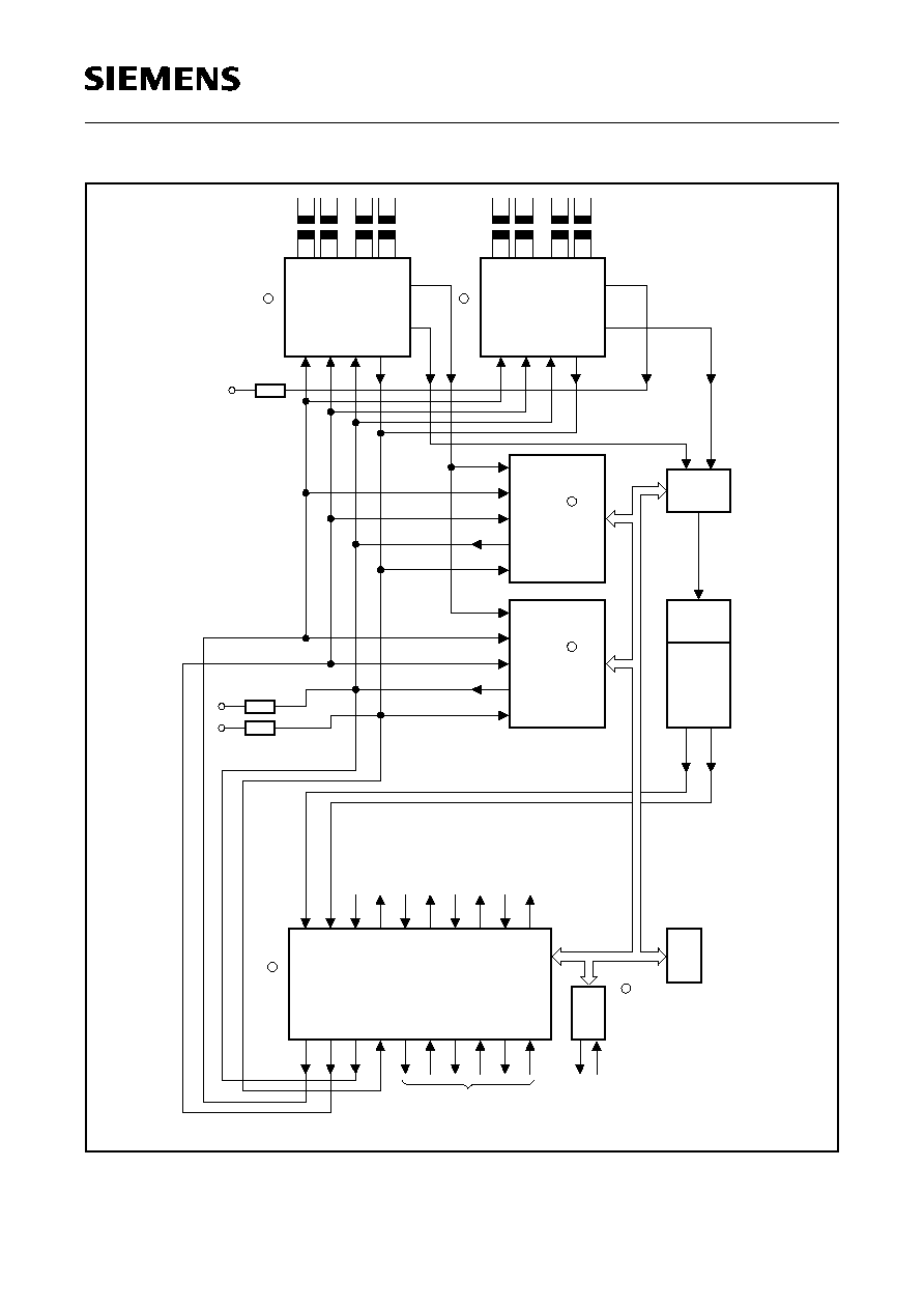
PEB 2055
PEF 2055
Application Hints
Semiconductor Group
235
Figure 82
PBX Trunk Card for Multiple Basic Rate Trunk Lines Using the QUAT
ģ
-S
ITS09554
1k
k
1
+5 V
+5 V
4096 kHz
8 kHz
2048 kbit/s or
4096 kbit/s
IOM -2
4x
P
PDC
PFS
3
DD
3
DU
DD
2
DU
2
1
DU
1
DD
0
DU
0
DD
FSC
DCL
EPIC
Layer 1
Interface
SD0X
ESC
DCL
CDR
SD0R
IDEC
IDEC
SD0R
CDR
DCL
ESC
SD0X
To PCM
Backplane
Clock
Generator
ID
ID
FSC
DCL
CLK
1
DRDY
LT-T
Mode
ISDN
T Interface
I
O
O
I
T Interface
ISDN
QUAT -S
Mode
LT-T
DRDY
1
CLK
DCL
FSC
ID
ID
2048 kbit/s
2048 kbit/s
+5 V
8 kHz
4096 kHz
4096 kHz
8 kHz
1536 kHz
Ports
k
1
Clock Source:
T Line with Layer 1
activated
RxD0
TxD0
TxD1
RxD1
TxD2
RxD2
TxD3
RxD3
HSCX
Highway
Signaling
M
U
X
P
L
L
Ķ
R
QUAT -S
R
R
R
R
R

PEB 2055
PEF 2055
Application Hints
Semiconductor Group
236
Initialization values for the IDEC that controls the lower 4 channels of the IOM-2
interface:
IDEC
ģ
CCR
= 1000 0010B =
82
H
IOM-2 mode, IOM ch. 0 - 3, double clock rate,
256 bits/frame
A_MODE
= 0000 1100B =
0C
H
uncond. trans., 16 kbit/s ch., channel and
receiver active
A_TSR
= 0000 1100B =
0C
H
ch. A time slot position: D channel of IOM ch. 0
B_MODE
= 0000 1100B =
0C
H
uncond. trans., 16 kbit/s ch., channel and
receiver active
B_TSR
= 0001 1100B =
1C
H
ch. B time slot position: D channel of IOM ch. 1
C_MODE
= 0000 1100B =
0C
H
uncond. trans., 16 kbit/s ch., channel and
receiver active
C_TSR
= 0010 1100B =
2C
H
ch. C time slot position: D channel of IOM ch. 2
D_MODE
= 0000 1100B =
0C
H
uncond. trans., 16 kbit/s ch., channel and
receiver active
D_TSR
= 0011 1100B =
3C
H
ch. D time slot position: D channel of IOM ch. 3
Initialization values for the IDEC that controls the upper 4 channels of the IOM-2
interface:
IDEC
ģ
CCR
= 1000 0010B =
A2
H
IOM-2 mode, IOM ch. 4-7, double clock rate,
256 bits/frame
A_MODE
= 0000 1100B =
0C
H
uncond. trans., 16 kbit/s ch., channel and
receiver active
A_TSR
= 0100 1100B =
4C
H
ch. A time slot position: D channel of IOM ch. 4
B_MODE
= 0000 1100B =
0C
H
uncond. trans., 16 kbit/s ch., channel and
receiver active
B_TSR
= 0101 1100B =
5C
H
ch. B time slot position: D channel of IOM ch. 5
C_MODE
= 0000 1100B =
0C
H
uncond. trans., 16 kbit/s ch., channel and
receiver active
C_TSR
= 0110 1100B =
6C
H
ch. C time slot position: D channel of IOM ch. 6
D_MODE
= 0000 1100B =
0C
H
uncond. trans., 16 kbit/s ch., channel and
receiver active
D_TSR
= 0111 1100B =
7C
H
ch. D time slot position: D channel of IOM ch. 7
The ELIC initialization is the same as for the IOM-2 application described previously in
this chapter.

PEB 2055
PEF 2055
Application Hints
Semiconductor Group
237
If the D-channel access procedure is programmed, the IDEC MODE registers must
additionally be programmed accordingly i.e. for each channel MODE = 2C
H
(instead
of 0C
H
).
Example
In a first step, the QUAT-S in IOM port 0, ch. 0 ... 3 is programmed via the IOM-2 monitor
handler to the LT-T mode:
W:OMDR
= EE
H
; activation ELIC with handshake protocol enabled
W:MFSAR
= 04
H
; monitor address of IOM port 0, channel 0
W:CMDR
= 01
H
; reset MFFIFO
R:STAR
= 25
H
; MFFIFO write access enabled
W:MFFIFO
= 81
H
; select QUAT-S Configuration Register
W:MFFIFO
= 41
H
; set LT-T mode, output CLK1
W:CMDR
= 04
H
; transmit MFFIFO content
R:ISTA
= 20
H
; MFFI interrupt
W:MFSAR
= 0C
H
; monitor address of IOM port 0, channel 1
W:CMDR
= 01
H
; reset MFFIFO
R:STAR
= 25
H
; MFFIFO write access enabled
W:MFFIFO
= 81
H
; select QUAT-S Configuration Register
W:MFFIFO
= 01
H
; set LT-T mode
W:CMDR
= 04
H
; transmit MFFIFO content
R:ISTA
= 20
H
; MFFI interrupt
W:MFSAR
= 14
H
; monitor address of IOM port 0, channel 2
W:CMDR
= 01
H
; reset MFFIFO
R:STAR
= 25
H
; MFFIFO write access enabled
W:MFFIFO
= 81
H
; select QUAT-S Configuration Register
W:MFFIFO
= 01
H
; set LT-T mode
W:CMDR
= 04
H
; transmit MFFIFO content
R:ISTA
= 20
H
; MFFI interrupt
W:MFSAR
= 1C
H
; monitor address of IOM port 0, channel 3
W:CMDR
= 01
H
; reset MFFIFO
R:STAR
= 25
H
; MFFIFO write access enabled
W:MFFIFO
= 81
H
; select QUAT-S Configuration Register
W:MFFIFO
= 01
H
; set LT-T mode
W:CMDR
= 04
H
; transmit MFFIFO content
R:ISTA
= 20
H
; MFFI interrupt

PEB 2055
PEF 2055
Application Hints
Semiconductor Group
238
5.9.2.2 Small PBX
Figure 83 shows a realization example of a small PBX. If the total number of lines
(internal or external) is smaller than the capacity of the EPIC (32
◊
(2
◊
B + D) or 64
◊
B),
the PCM interface of the EPIC need not to be connected to a switching network since all
the B (and D) channel switching can be done inside the EPIC. In this special case, it is
sufficient to apply only a PCM clock to the EPIC, the PCM frame synchronization signal
(8 kHz) can be omitted. The IOM-2 clock and framing signals DCL and FSC are still
generated correctly by the EPIC. The STAR:PSS bit should then not be evaluated: it
stays at logical 0 all the time.
The PBX shown in the figure 83 offers 8 analog (t/r) subscriber lines, realized with two
quadruple codec/filter devices SICOFI-4 (PEB 2465). These can of course be replaced
by any IOM-2 compatible layer-1 device if digital lines are required. Any mixture of
codecs and digital layer-1 devices is also feasible.
The figure 83 also shows a digital trunk line (external line) which is realized with a U
k
-
layer-1 device, IEC-Q (PEB 2091), operated in NT-PABX mode. The PBX can therefore
be connected directly to the U
k
interface coming from the CO. The NT-PABX mode of
the U
k
- layer-1 devices is similar to the LT-T mode of the S layer-1 devices: in both cases
the layer-1 device delivers a reference clock which is synchronous to the received S or
U
k
- frame and that can be used to synchronize the local PBX clock generator. Any phase
differences between the local IOM-2 frame and the received S or U
k
- frame are
compensated by an elastic buffer inside the layer-1 devices.
Since the digital trunk line also needs a D channel handler, an ISDN Communication
Controller (ICC; PEB 2070) is assigned to that IOM-2 channel.

PEB 2055
PEF 2055
Application Hints
Semiconductor Group
239
Figure 83
Small PBX with SICOFI
ģ
-4 and IEC-Q
ITS09555
EPIC
DCL
FSC
DD0
DU0
DD1
DU1
DU2
DD2
DU3
DD3
PFS
PDC
P
DCL
FSC
DIN
DOUT
Lines
Filter Device
DOUT
DIN
FSC
DCL
IEC-Q
DCL
FSC
D
D
IN
OUT
SICOFI -4
Quadruple Codec
Analog
Analog
Lines
Quadruple Codec
Filter Device
1 k
k
1
+5 V
+5 V
4096 kHz
8 kHz
2048 kbit/s
2048 kbit/s
PLL
CLS
NT-PABX
Mode
4096 kHz
ISDN
U
to Central
Office
Trunk Line
PCM
Interface:
Not Used
IOM -2 Ports
4 x
SICOFI -4
k
Interface
Controller
Layer-2
IDP0
IDP1
FSC
DCL
ICC
RxD0
TxD0
TxD1
RxD1
TxD2
RxD2
TxD3
RxD3
Ķ
R
R
R
R

PEB 2055
PEF 2055
Application Hints
Semiconductor Group
240
5.9.3
Miscellaneous
5.9.3.1 Interfacing the EPIC
ģ
to a MUSAC
TM
The PCM interface of the EPIC can easily be connected to the Multipoint Switching and
Conferencing circuit MUSAC (PEB 2245) when using the set-up and PCM timing as
shown in figure 84. This configuration can then for example be used in a PBX to
implement conferencing functions for up to 21 simultaneous conferences.
Figure 84
Interconnection Example EPIC
ģ
- MUSAC
TM
ITS09556
EPIC
DCL
FSC
DD0
DU0
DD1
DU1
DU2
DD2
DU3
DD3
4 x 2048 kbit/s
PFS
PDC
4 x IOM -2 Ports
4096 kbit/s
SP
CLK
OUT0
IN0
MUSAC
P
IN1
IN2
IN3
IN4
IN5
IN6
IN7
OUT3
OUT2
OUT1
PCM Backplane
4096 kHz
8 kHz
RxD0
TxD0
TxD1
RxD1
TxD2
RxD2
TxD3
RxD3
TM
Ķ
R
R

PEB 2055
PEF 2055
Application Hints
Semiconductor Group
241
Figure 85
Timing Example to Interconnect the EPIC
ģ
and the MUSAC
TM
on an IOM
ģ
-2 Line
Card
The following values must be programmed to the PCM and CFI registers of the EPIC
and to the MOD and CFR registers of the MUSAC to obtain the desired PCM and IOM-2
timing:
EPIC
ģ
PMOD
= 0100 0100
B
=
44
H
PCM mode 1, single rate clock, PFS
evaluated with falling clock edge, input
selection RxD0 and RxD3, PCM comparison
disabled
PBNR
= 1111 1111
B
=
FF
H
512 bits (64 ts) per PCM frame
POFD
= 1111 0000
B
=
F0
H
PFS marks downstream PCM TS0, bit 6
POFU
= 0001 1000
B
=
18
H
PFS marks upstream PCM TS0, bit 6
PCSR
= 0100 0101
B
=
45
H
PCM data received with falling, transmitted
with rising clock edge
CMD1
= 0010 0000
B
=
20
H
PDC/PFS clock source, PFS evaluated with
falling clock edge, prescaler = 1, CFI mode 0
CMD2
= 1101 0000
B
=
D0
H
FC mode 6, double rate clock, CFI data
transmitted with rising, received with falling
clock edge
CBNR
= 1111 1111
B
=
FF
H
256 bits (32 ts) per CFI frame
ITT09557
TS63, Bit 0
Bit 7
TS0,
MUSAC/EPIC :
SP/PFS
CLK/PDC
OUT#/TxD#
IN#/RxD#
TS0, Bit 6
TS0, Bit 5
TS0, Bit 4
TS0, Bit 3
Bit 3
TS0,
Bit 4
TS0,
Bit 5
TS0,
Bit 6
TS0,
TS0, Bit 7
Bit 0
TS63,
R

PEB 2055
PEF 2055
Application Hints
Semiconductor Group
242
CTAR
= 0000 0010
B
=
02
H
PFS marks downstream CFI TS0
CBSR
= 0010 0000
B
=
20
H
PFS marks downstream CFI bit 6, upstream
bits not shifted
CSCR
= 0000 0000
B
=
00
H
64, 32, 16 kbit/s channels located on CFI bits
7 ... 0, 7 ... 4, 7 ... 6
MUSAC
TM
MOD
= 0100 0100
B
=
03
H
input mode 8
◊
4M, output mode 4
◊
4M
CFR
= 1111 1111
B
=
DE
H
4.096 MHz device clock, conferencing
mode, A-law, even bits inverted
5.9.3.2 Space and Time Switch for 16 kbit/s Channels
The EPIC is optimized for the space and time switching of 64 kbit/s channels (8 bit time
slots). The switching of 32 and 16 kbit/s subchannels is also supported, but these
channels can only be freely selected at the PCM interface. At the CFI, only one
subchannel per 8 bit time slot can be switched (see chapter 5.4.2). Usually, this is
sufficient because on the IOM-2 interface, only one 16 kbit/s D channel per time slot
needs to be switched. Up to four D channels may then be combined into a single 8 bit
PCM time slot.
If a completely flexible space and time switch for contiguous 16 kbit/s channels is
required, the following method can be used:
The four CFI ports are connected in parallel as shown in figure 86. Each CFI port is
programmed via the CFI subchannel register (CSCR) to handle a different 2 bit subtime
slot position. With this configuration, any mixture of 16, 32 and 64 kbit/s channels may
be switched between the CFI and the PCM interfaces. Up to 128 16 kbit/s channels per
direction can be handled by the EPIC. The switching software must select the CFI port
number according to the required CFI subchannel position for each CFI - PCM
connection. The PCM subchannel position is selected via the control memory (CM) code
field (see table 24). For 32 and 64 kbit/s connections, only one CFI port of a given time
slot may be programmed in order to avoid collisions on the CFI "bus".

PEB 2055
PEF 2055
Application Hints
Semiconductor Group
243
Figure 86
Non-blocking Space and Time Switch for 16 kbit/s Channels
ITS09558
EPIC
DCL
FSC
DD0
DU0
DD1
DU1
DU2
DD2
DU3
DD3
DD
DU
128 x 16 kbit/s
PFS
PDC
128 x 16 kbit/s
SC01...00 = 11
DD0/DU0
DD1/DU1
10
=
SC11...10
SC21...20 = 01
DD2/DU2
DD3/DU3
00
=
SC31...30
CSCR = B
DD/DU
1 H
RxD3
TxD3
RxD2
TxD2
RxD1
TxD1
TxD0
RxD0
R
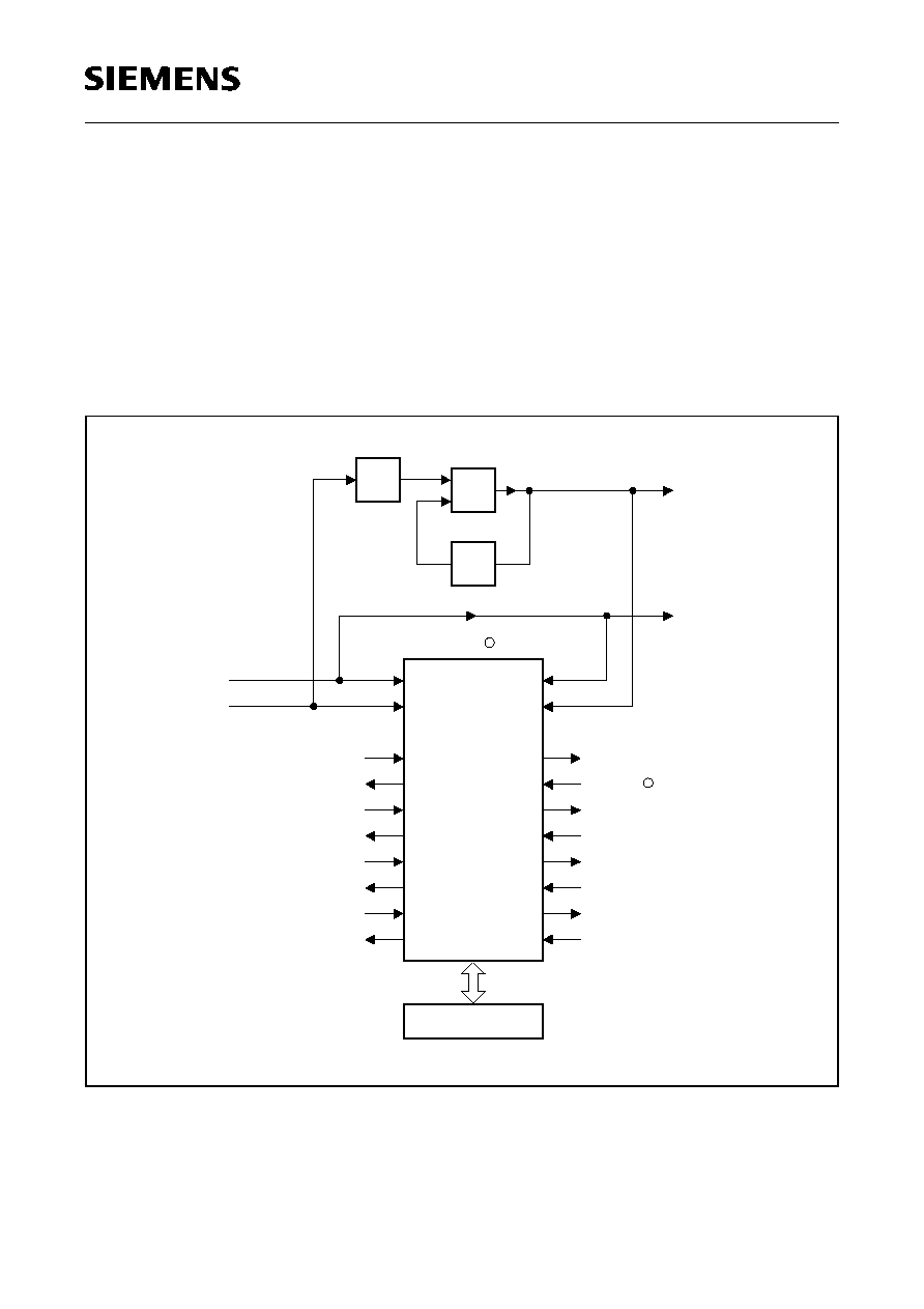
PEB 2055
PEF 2055
Application Hints
Semiconductor Group
244
5.9.3.3 Interfacing an IOM
ģ
-2 Terminal Mode Interface to a 2.048 Mbit/s PCM
Backplane
For some applications, it is necessary to connect IOM-2 terminal devices (e.g. ARCOFI,
PSB 2160) to a PCM backplane. In such a configuration, the EPIC can be used as a rate
adaptor between these two differing data rates. Since the internal prescalers of the EPIC
cannot be used to convert the 2.048 Mbit/s (PCM) into 768 kbit/s (IOM-2 terminal mode),
an external clock converting circuit as shown in figure 87 has to be built up. A PLL
controlled oscillator generates the IOM-2 data clock of 1.536 MHz by comparing the
PCM clock divided by 4 with the DCL clock divided by 3.
Figure 87
Interface Circuit to adapt the IOM
ģ
-2 (768 kbit/s) and PCM (2.048 Mbit/s) Data Rates
DD3
DU3
DD2
DU2
DD1
DU1
DU0
DD0
P
TxD3
ITS09559
RxD3
768 kbit/s
DCL
FSC
RxD2
TxD2
TxD1
RxD1
TxD0
RxD0
PDC
PFS
EPIC
8 kHz
2.048 MHz
2.048 Mbit/s
FSC
IOM -2 Ports
4 x
(terminal mode)
x
4
PLL
4
DCL
1.536 MHz
3
Ķ
R
R

PEB 2055
PEF 2055
Application Hints
Semiconductor Group
245
Figure 88
IOM
ģ
-2 (768 kbit/s) and PCM (2.048 Mbit/s) Timing Example
If the PCM input clock timing of figure 88 applies, the following values have to be written
to the EPIC to obtain the correct PCM and CFI timing:
EPIC
ģ
PMOD
= 0010 0000
B
=
20
H
PCM mode 0, single rate clock, PFS
evaluated with rising clock edge,
PCM comparison disabled
PBNR
= 1111 1111
B
=
FF
H
256 bits (32 ts) per PCM frame
POFD
= 1111 0000
B
=
F0
H
PFS marks downstream PCM TS0, bit 7
POFU
= 0001 1000
B
=
18
H
PFS marks upstream PCM TS0, bit 7
PCSR
= 0000 0001
B
=
01
H
PCM data received with falling, transmitted
with rising clock edge
CMD1
= 1110 0000
B
=
E0
H
DCL/FSC clock source, FSC evaluated with
rising clock edge, prescaler = 1, CFI mode 0
CMD2
= 0000 0000
B
=
00
H
CFI data transmitted with rising, received with
falling clock edge
CBNR
= 0101 1111
B
=
5F
H
96 bits (12 ts) per CFI frame
CTAR
= 0000 0010
B
=
02
H
PFS marks downstream CFI TS0
CBSR
= 0010 0000
B
=
20
H
PFS marks downstream CFI bit 7, upstream
bits not shifted
CSCR
= 0000 0000
B
=
00
H
64, 32, 16 kbit/s channels located on CFI bits
7 ... 0, 7 ... 4, 7 ... 6
ITT09560
PFS/FSC
PDC
TxD#
RxD#
DCL
DU#
DD#
TS0, Bit 7
TS31 Bit 0
,
, Bit 1
TS31
,Bit 7
TS0
TS0 Bit 6
,
TS0 Bit 5
,
TS0 Bit 4
,
TS0 Bit 3
,
TS0 Bit 2
,
TS0 Bit 1
,
TS0 Bit 0
,
TS0 Bit 7
,
TS0 Bit 6
,
Bit 4
TS0,
Bit 0
TS12,
Bit 6
TS0,
Bit 5
TS0,
,Bit 6
TS0
,Bit 7
TS0
,Bit 0
TS0
,Bit 1
TS0
,Bit 2
TS0
,Bit 3
TS0
,Bit 4
TS0
,Bit 5
TS0
,Bit 6
TS0
TS0 Bit 7
,
TS31 Bit 1
,
,Bit 0
TS31
TS0, Bit 5
TS0, Bit 6
TS12, Bit 0
TS0, Bit 4
Bit 7
TS0,
(8 kHz)
(2.048 MHz)
(2.048 Mbit/s)
(2.048 Mbit/s)
(1.536 MHz)
(768 kbit/s)
(768 kbit/s)

PEB 2055
PEF 2055
Electrical Characteristics
Semiconductor Group
246
6
Electrical Characteristics
Absolute Maximum Ratings
Note: Stresses above those listed here may cause permanent damage to the device.
Exposure to absolute maximum ratings conditions for extended periods may affect
device reliability.
Note: The listed characteristics are ensured over the operating range of the integrated
circuit. Typical characteristics specify mean values expected over the production
spread. If not otherwise specified, typical characteristics apply at
T
A
= 25
į
C and
the given supply voltage.
Parameter
Symbol
Limit Values
Unit
min.
max.
Ambient temperature under bias: PEB
PEF
T
A
T
A
0
≠ 40
70
85
į
C
į
C
Storage temperature
T
stg
-
65
125
į
C
Voltage on any pin with respect to ground
V
S
-
0.4
V
DD
+ 0.4
V
Maximum voltage on any pin
V
max
6
V
Parameter
Symbol
Limit Values
Unit Test Condition
min.
max.
L-input voltage
V
IL
-
0.4
0.8
V
H-input voltage
V
IH
2.2
V
DD
+ 0.4
L-output voltage
V
OL
0.45
V
I
OL
= 7 mA
(pins DU3..0,
DD3..0)
I
OL
= 2 mA
(all other)
H-output voltage
H-output voltage
V
OH
V
OH
2.4
V
DD
-
0.5
V
V
I
OH
=
-
400
Ķ
A
I
OH
=
-
100
Ķ
A
Power
supply
current
operational
I
CC
9.5
6.5
mA
mA
V
DD
= 5 V,
inputs at 0 V
or
V
DD
,
no output loads
PDC > 4.096 MHz
PDC
4.096 MHz
Input leakage current
Output leakage current
I
LI
I
LO
10
10
Ķ
A
Ķ
A
0 V <
V
IN
<
V
DD
to 0 V
0 V <
V
OUT
<
V
DD
to 0 V

PEB 2055
PEF 2055
Electrical Characteristics
Semiconductor Group
247
AC Characteristics
Ambient temperature under bias range,
V
DD
= 5 V
Ī
5 %.
Inputs are driven to 2.4 V for a logical "1" and to 0.4 V for a logical "0".
Timing measurements are made at 2.0 V for a logical "1" and at 0.8 V for a logical "0".
The AC-testing input/output wave forms are shown below.
Figure 89
I/O-Wave Form for AC-Test
Capacitances
Parameter
Symbol
Limit Values
Unit
min.
max.
Input capacitance
C
IN
10
pF
Output capacitance
C
OUT
15
pF
I/O
C
I/O
20
pF
Under
Device
Test
ITS05853
= 150 pF
C
L
2.4 V
0.4 V
Test Points
2.0 V
0.8 V
0.8 V
2.0 V

PEB 2055
PEF 2055
Electrical Characteristics
Semiconductor Group
248
Bus Interface Timing
Parameter
Symbol
Limit Values
Unit
min.
max.
R or W set-up to DS
t
DSD
0
ns
RD-pulse width
t
RR
120
ns
RD-control interval
t
RI
70
ns
Data output delay from RD
t
RD
100
ns
Data float delay from RD
t
DF
25
ns
WR-pulse width
t
WW
60
ns
WR-control interval
t
WI
70
ns
Data set-up time to WRxCS, DSxCS
t
DW
30
ns
Data hold time from WRxCS, DSxCS
t
WD
10
ns
ALE-pulse width
t
AA
30
ns
Address set-up time to ALE
t
AL
10
ns
Address hold time from ALE
t
LA
15
ns
ALE set-up time to WR, RD
t
ALS
0
ns
Address set-up time to WR, RD
t
AS
10
ns
Address hold time from WR
t
AH
40
ns
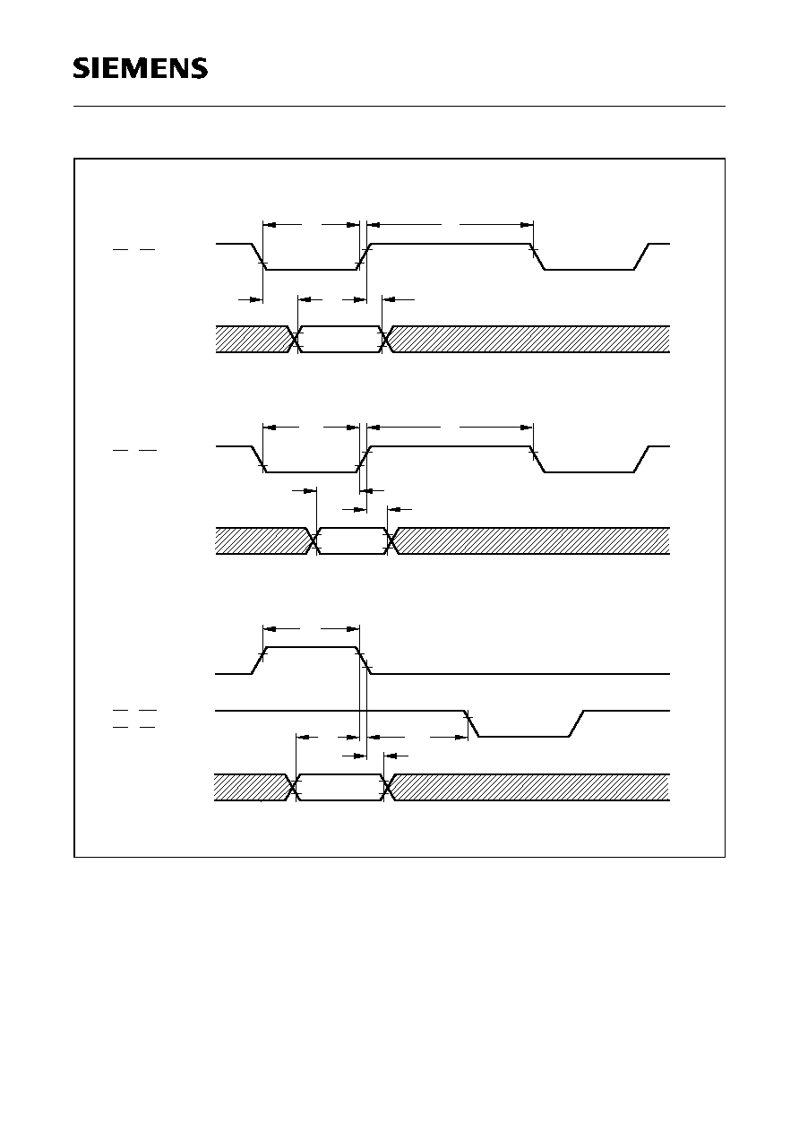
PEB 2055
PEF 2055
Electrical Characteristics
Semiconductor Group
249
Figure 90
Siemens/Intel Bus Mode
ITT09561
t
RR
t
RI
t
RD
t
DF
Data
CS x RD
mP Read Cycle
0-07
D
t
WW
t
WI
t
DW
t
WD
Data
mP Write Cycle
0-07
WR
x
CS
D
Address
t
AL
t
LA
WR
x
CS
CS x RD
Address Timing
Multiplexed Bus Mode
t
AA
t
ALS
ALE
AD0 - AD7
,

PEB 2055
PEF 2055
Electrical Characteristics
Semiconductor Group
250
Figure 91
Siemens/Intel Bus Mode
ITT09562
Address
t
AS
t
AH
Address Timing,
Demultiplexed Bus Mode
RD
x
CS
CS x WR
A0 - A3
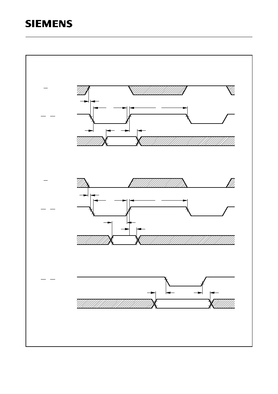
PEB 2055
PEF 2055
Electrical Characteristics
Semiconductor Group
251
Figure 92
Motorola Bus Mode
t
DSD
t
RR
t
RI
R/W
CS x DS
mP Read Cycle
Data
t
RD
t
DF
D0 - D7
- 7
D
Write Cycle
mP
0
D
W
/
R
Data
WD
t
DW
t
WI
t
WW
t
DSD
t
Address Timing
Address
AS
t
AH
t
ITT09563
A0 A3
-
DS
x
CS
DS
x
CS

PEB 2055
PEF 2055
Electrical Characteristics
Semiconductor Group
252
PCM and Configurable Interface Timing
1) Parameter can be estimated to: 20 ns + 0.25 ns x [C
L
]
2) The max. difference between T
DCD
and T
CDF
/ T
CDR
is 60 ns / 35 ns
Parameter
Symbol Limit Values Unit Test Condition
min.
max.
Clock period
t
CP
240
ns
Clock frequency
4096 kHz
Clock period low
t
CPL
80
ns
Clock period high
t
CPH
100
ns
Clock period
t
CP
120
ns
Clock frequency
> 4096 kHz
Clock period low
t
CPL
50
ns
Clock period high
t
CPH
50
ns
Frame set-up time to clock
t
FS
25
ns
Frame hold time from clock
t
FH
50
ns
Data clock delay
t
DCD
125
ns
2)
Serial data input set-up time
(falling clock edge)
t
S
7
ns
PCM-input data
frequency > 4096 kbit/s
Serial data input set-up time
(rising clock edge)
t
S
15
ns
Serial data hold time
t
H
35
ns
Serial data input set-up time
t
S
15
ns
PCM-input data
frequency
4096 kbit/s
Serial data hold time
t
H
55
ns
Serial data input set-up time
t
S
20
ns
CFI-input data
frequency > 4096 kbit/s
Serial data hold time
t
H
50
ns
Serial data input set-up time
t
S
0
ns
CFI-input data
frequency
4096 kbit/s
Serial data hold time
t
H
75
ns
PCM-serial data output delay
t
D
55
ns
1)
Tristate control delay
t
T
60
ns
1)
CFI-serial data output delay
t
CDF
65
ns
Falling clock edge
2)
CFI-serial data output delay
t
CDR
≠
90
ns
Rising clock edge
2)

PEB 2055
PEF 2055
Electrical Characteristics
Semiconductor Group
253
Figure 93
Configurable Interface Timing, CMD:CSP1,0 = 10 (prescaler divisor = 1)
ITD05868
1 Bit of Frame
st
t
FH
t
FH
t
FS
t
FS
t
FS
t
FH
t
FH
t
CDF
t
CDR
t
S
t
H
Last Bit of Frame
t
CDF
t
H
t
S
H
t
S
t
t
S
t
H
S
t
t
H
t
CP
t
CPL
CPH
t
t
FS
st
1 Bit of Frame
st
1 Bit of Frame
CDR
t
CDF
t
Last Bit of the Frame
CDF
t
t
CDR
DCD
t
DCD
t
DCD
t
PDC/DCL
CMD1 : CMD1, 0 = 01 or 10
PFS
FSC
(CMD1 : CSS, CSM = 1,0)
FSC
PFS
(PMOD : PSM = 0; CMD1 : CSS = 0)
DD (CMD2 : CXF = 0)
DCL
(CMD1 = 0x1000xx)
(CMD2 : DOC = 1)
FSC
(CMD2 : FC (2 : 0) = 011)
CMD1 : CMD1, 0 = 00
CMD1 : CMD1, 0 = 11
(PMOD : PSM = 1; CMD1 : CSS = 0)
(CMD1 : CSS, CSM = 1,1)
2 Bit of Frame
nd
3 Bit of Frame
rd
DU (CMD2 : CRR = 0)
DD (CMD2 : CXF = 1)
DU (CMD2 : CRR = 1)
DD (CMD2 : CXF = 0)
DU (CMD2 : CRR = 0)
DD (CMD2 : CXF = 1)
DU (CMD2 : CRR = 1)
1 Bit of Frame
st
1 Bit of Frame
st
1 Bit of Frame
st
1 Bit of Frame
st
1 Bit of Frame
st
1 Bit of Frame
st
1 Bit of Frame
st
DD (CMD2 : CXF = 1)
DU (CMD2 : CRR = 0)
DD (CMD2 : CXF = 0)

PEB 2055
PEF 2055
Electrical Characteristics
Semiconductor Group
254
Figure 94
Configurable Interface Timing, CMD:CSP1,0 = 01 (prescaler divisor = 1,5)
ITD05869
t
FS
t
FH
t
DF
t
S
t
H
t
DF
t
H
t
S
H
t
S
t
t
S
t
H
S
t
t
H
t
CP
t
CPL
CPH
t
DR
t
DF
t
DF
t
t
DR
DCD
t
DCD
t
t
FS
FH
t
FH
t
t
FS
t
FS
t
FH
t
DCD
1 Bit of Frame
st
Last Bit of Frame
st
1 Bit of Frame
1 Bit of Frame
Last Bit of the Frame
PDC/DCL
CMD1 : CMD1, 0 = 01 or 10
PFS
FSC
(CMD1 : CSS, CSM = 1,0)
FSC
PFS
(PMOD : PSM = 0; CMD1 : CSS = 0)
DD (CMD2 : CXF = 0)
DCL
(CMD1 = 0x1000xx)
(CMD2 : COC = 1)
FSC
CMD1 : CMD1, 0 = 00
CMD1 : CMD1, 0 = 11
(PMOD : PSM = 1; CMD1 : CSS = 0)
(CMD : CSS, CSM = 1,1)
2 Bit of Frame
nd
3 Bit of Frame
rd
DU (CMD2 : CRR = 0)
DD (CMD2 : CXF = 1)
DU (CMD2 : CRR = 1)
DD (CMD2 : CXF = 0)
DU (CMD2 : CRR = 0)
DD (CMD2 : CXF = 1)
DU (CMD2 : CRR = 1)
1 Bit of Frame
1 Bit of Frame
1 Bit of Frame
st
1 Bit of Frame
1 Bit of Frame
st
1 Bit of Frame
st
1 Bit of Frame
st
DD (CMD2 : CXF = 1)
DU (CMD2 : CRR = 0)
DD (CMD2 : CXF = 0)
st
st
st
st

PEB 2055
PEF 2055
Electrical Characteristics
Semiconductor Group
255
Figure 95
Configurable Interface Timing, CMD:CSP1,0 = 00 (prescaler divisor = 2)
ITD05870
t
FH
t
FS
t
FH
t
FH
t
DR
t
CR
t
S
t
H
t
DR
t
H
t
S
H
t
S
t
t
S
t
H
S
t
t
H
t
FS
DR
t
DR
t
DR
t
t
DR
DCD
t
DCD
t
DCD
t
CP
t
CPL
t
t
CPH
t
FS
t
FS
FH
t
1 Bit of Frame
st
Last Bit of Frame
st
1 Bit of Frame
1 Bit of Frame
Last Bit of the Frame
PDC/DCL
CMD1 : CMD1, 0 = 01 or 10
PFS
FSC
(CMD1 : CSS, CSM = 1,0)
FSC
PFS
(PMOD : PSM = 0; CMD1 : CSS = 0)
DD (CMD2 : CXF = 0)
DCL
(CMD1 = 0x1000xx)
COC = 1
FSC
CMD1 : CMD1, 0 = 00
CMD1 : CMD1, 0 = 11
(PMO D : PSM = 1; CMD1 : CSS = 0)
(CMD1 : CSS, CSM = 1,1)
2 Bit of Frame
nd
3 Bit of Frame
rd
DU (CMD2 : CRR = 0)
DD (CMD2 : CXF = 1)
DU (CMD2 : CRR = 1)
DD (CMD2 : CXF = 0)
DU (CMD2 : CRR = 0)
DD (CMD2 : CXF = 1)
DU (CMD2 : CRR = 1)
1 Bit of Frame
1 Bit of Frame
1 Bit of Frame
st
1 Bit of Frame
1 Bit of Frame
st
1 Bit of Frame
st
1 Bit of Frame
st
DD (CMD2 : CXF = 1)
DU (CMD2 : CRR = 0)
DD (CMD2 : CXF = 0)
st
st
st
st

PEB 2055
PEF 2055
Electrical Characteristics
Semiconductor Group
256
Figure 96
PCM-Interface Timing
ITD05871
1 Bit of Frame
st
2 Bit of Frame
nd
3 Bit of Frame
rd
t
FH
t
FH
t
FS
t
FS
t
FS
t
FH
t
FH
t
D
t
t
H
t
T
t
H
t
S
H
t
S
t
t
S
t
H
t
CP
t
CPL
CPH
t
t
FS
D
t
D
t
PDC
PMOD : PCR = 0
PFS (PMOD : PSM = 0)
D
t
S
t
T
t
T
t
T
PFS (PMOD : PSM = 1)
TxD (PCSR : URE = 1)
TSC (PCSR : URE = 1)
RxD (PCSR : 'DRE' = 0)
TxD (PCSR : URE = 0)
TSC (PCSR : URE = 0)
TxD (PCSR : URE = 1)
TSC (PCSR : URE = 1)
RxD (PCSR : 'DRE' = 0)
TxD (PCSR : URE = 0)
TSC (PCSR : URE = 0)
RxD (PCSR : 'DRE' = 1)
PMOD : PCR = 0
RxD (PCSR : 'DRE' = 1)
1 Bit of Frame
st
1 Bit of Frame
st
1 Bit of Frame
st
1 Bit of Frame
st
1 Bit of Frame
st
1 Bit of Frame
st
1 Bit of Frame
st
1 Bit of Frame
st
1 Bit of Frame
st
1 Bit of Frame
st

PEB 2055
PEF 2055
Package Outlines
Semiconductor Group
257
7
Package Outlines
G
P
M05249
P-LCC-44-1
(Plastic Leaded Chip Carrier)
Sorts of Packing
Package outlines for tubes, trays etc. are contained in our
Data Book "Package Information"
Dimensions in mm
SMD = Surface Mounted Device

PEB 2055
PEF 2055
Appendix
Semiconductor Group
258
8
Appendix
8.1
Working Sheets
The following pages contain some working sheets to facilitate the programming of the
EPIC. For several tasks (i.e. initialization, time slot switching, ...) the corresponding
registers are summarized in a way the programmer gets a quick overview on the
registers he has to use.
8.1.1
Register Summary for EPIC
ģ
Initialization
Figure 97
EPIC
ģ
Initialization Register Summary (working sheet)
PCM Interface
PMOD
PCM Mode Register
RW, 20
H
(0
H
+ RBS = 1), reset-val. = 00
PMD0..1 = PCM Mode, 00 = 0, 01 = 1, 10 = 2
PCR = PCM Clock Rate:
0 = equal to PCM data rate
1 = double PCM data rate (not for mode 2)
PSM = PCM Synchron Mode:
0 = frame synchr. with falling edge,
1 = rising edge of PDC
AIS0..1 = Alternative Input Section: (PCM mode dependent)
Mode 0:
AIS = 0
Mode 1:
AIS0 = 0: RXD1 = IN0, AIS0 = 1: RXD0 = IN0
AIS1 = 0: RXD3 = IN1, AIS1 = 1: RXD2 = IN1
Mode 2:
AIS0 = 0
AIS1 = 0: RXD3 = IN, AIS = 1: RXD2 = IN
AIC0..1 = Alternative Input Comparison: (PCM mode dependent)
Mode 0, 1: AIC0 = 0: no comparison, AIC0 = 1: RXD0 == RXD1
AIC1 = 0: no comparison, AIC1 = 1: RXD2 == RXD3
Mode 2:
AIC0 = 0:
AIC1 = 0: no comparison, AIC1 = 1: RXD2 == RXD3
PBNR
PCM Bit Number Register
RW, 22
H
(1
H
+ RBS = 1), reset-val. = FF
BNR0..7 = Bit Number per Frame (mode dependent)
Mode 0: BNR = number of bits ≠ 1
Mode 1: BNR = (number of bits)/2 ≠ 1
Mode 2: BNR = (number of bits)/4 ≠ 1
PMD
PCR
PSM
AIS
AIC
BNR

PEB 2055
PEF 2055
Appendix
Semiconductor Group
259
Figure 98
EPIC
ģ
Initialization Register Summary (working sheet)
POFD
PCM Offset Downstream Register RW, 24
H
(2
H
+ RBS = 1), reset-val. = 0
OFD2..9 = Offset Downstream (see PCSR for OFD0..1)
Mode 0: (BND ≠ 17 + BPF) mod BPF --> OFD2..9
Mode 1: (BND ≠ 33 + BPF) mod BPF --> OFD1..9
Mode 2: (BND ≠ 65 + BPF) mod BPF --> OFD0..9
BND = number of bits + 1 that the downstream frame start is left shifted relative to the
frame sync
BPF = number of bits per frame
Unused bits must be set to 0 !
POFU
PCM Offset Upstream Register
RW, 26
H
(3
H
+ RBS = 1), reset-val. = 0
OFU2..9 = Offset Upstream (see PCSR for OFU0..1)
Mode 0: (BND + 23 + BPF) mod BPF --> OFU2..9
Mode 1: (BND + 47 + BPF) mod BPF --> OFU1..9
Mode 2: (BND + 95 + BPF) mod BPF --> OFU0..9
BND = number of bits + 1 that the upstream frame is left shifted relative to the frame start
BPF = number of bits per frame
Unused bits must be set to 0 !
PCSR
PCM Clock Shift Register
RW, 28
H
(4
H
+ RBS = 1), reset-val. = 0
OFD0..1 = Offset Downstream (see POFD)
DRE = Downstream Rising Edge,
0 = receive data on falling edge,
1 = receive data on rising edge
OFU0..1 = Offset Upstream (see POFU)
URE = Upstream Rising Edge,
0 = send data on falling edge,
1 = send data on rising edge
OFD9..2
OFU9..2
0
OFD1..0
DRE
0
OFU1..0
URE

PEB 2055
PEF 2055
Appendix
Semiconductor Group
260
Figure 99
EPIC
ģ
Initialization Register Summary (working sheet)
CFI Interface
CMD1
CFI Mode Register 1
RW, 2C
H
(6
H
+ RBS = 1), reset-val. = 00
CSS = Clock Source Select,
0 = PDC/PFS used for CFI,
1= DCL/FSC are inputs
CSM = CFI Synchronization Mode:
1 = frame syncr. with rising edge,
0 = falling edge of DCL
if CSS = 0 ==> CMD1:CSM = PMOD:PSM !
CSP0..1 = Clock Source Prescaler: 00 = 1/2, 01 = 1/1.5, 10 = 1/1
CMD0..1 = CFI Mode: 00 = 0, 01 = 1, 10 = 2, 11 = 3
CIS0..1 = CFI Alternative Input Section
Mode 0, 3: CIS0..1 = 0
Mode 1, 2: CIS0: 0 = IN0 = DU0, 1 = IN0 = DU2
Mode 1: CIS1: 0 = IN1 = DU1, 1 = IN1 = DU3
CMD2
CFI Mode Register 2
RW, 2E
H
(7
H
+ RBS = 1), reset-val. = 00
For IOM
ģ
-2 CMD2 can be set to D0
H
FC0..2 = Framing Signal Output Control (CMD1:CSS = 0)
= 010 suitable for PBC, = 011 for IOM-2, = 110 IOM-2 and SLD
COC = Clock Output Control (CMD1:CSS = 0)
= 0 DCL = data rate,
= 1 DCL 2
◊
data rate (only mode 0 and 3 !)
CXF = CFI Transmit on Falling Edge: 0 = send on rising edge, 1 = send on falling DCL edge
CRR = CFI Receive on Rising Edge: 0 = receive on falling edge, 1 = send on rising DCL
edge
CBN8..9 = CFI Bit Number (see CBNR)
CBNR
CFI Bit Number Register
RW, 30
H
(8
H
+ RBS = 1), reset-val. = FF
CBN0..7 = CFI Bit Number per Frame ≠ 1 (see CMD2:CBN8..9)
CSS
CSM
CSP1..0
CMD1..0
CIS1..0
FC2..0
COC
CXF
CRR
CBN9..8
CBN

PEB 2055
PEF 2055
Appendix
Semiconductor Group
261
Figure 100
EPIC
ģ
Initialization Register Summary (working sheet)
CTAR
CFI Time Slot Adjustment Register RW, 32
H
(9
H
+ RBS = 1), reset-val. = 00
TSN0..6 = (number of time slots + 2) the DU and DD frame is left shifted relative to frame
start (see also CBSR)
CBSR
CFI Bit Shift Register
RW, 34
H
(A
H
+ RBS = 1), reset-val. = 00
CDS2..0: CFI Downstream/Upstream Bit Shift
Shift DU and DD frame:
000 = 2 bits right
001 = 1 bit right
010 = 6 bits left
011 = 5 bits left
100 = 4 bits left
101 = 3 bits left
110 = 2 bits left
111 = 1 bit left
Relative to PFS (if CMD1:CSS = 0)
Relative to FSC (if CMD1:CSS = 1)
CSCR
CFI Subchannel Register
RW, 36
H
(A
H
+ RBS = 1), reset-val. = 00
SC3 0..1 control port 3 (+ port 7 for CFI mode 3 (SLD))
SC2 0..1 control port 2 (+ port 6 for CFI mode 3 (SLD))
SC1 0..1 control port 1 (+ port 5 for CFI mode 3 (SLD))
SC0 0..1 control port 0 (+ port 4 for CFI mode 3 (SLD))
for 64 kBit/s channel: 00/01/10/11 = bits 7..0
for 32 kBit/s channel: 00/10 = bits 7..4,
01/11 = bits 3..0
0
TSN
0
CDS2..0
CUS3..0
CS3
CS2
CS1
CS0

PEB 2055
PEF 2055
Appendix
Semiconductor Group
262
8.1.2
Switching of PCM Time Slots to the CFI Interface (data downstream)
Figure 101
Switching of PCM Time Slots to the CFI Interface (working sheet)
ITD08110
Data Memory
PCM TS
ELIC,
R
EPIC
R
0
.
.
.
.
.
.
.
MAAR
CFI Port, TS
MADR
.
.
.
.
.
.
.
.
PCM Port, TS
Switching Command
0 1 1 1 0 0 0 1
MACR
Switching of 8 Bit Channels:
1
1 0 =
1 1 = 7, 6
0 0 1 0 =
=
1
1
0
0
MACR
.
.
.
.
1
1
1
0
.
.
.
.
.
.
.
.
MADR
MAAR
.
.
.
.
.
.
.
0
=
1
0
0 0 =
5, 4
3, 2
1, 0
Loop
0
Output
Disable
CFI TS
Loop
Direct
Switching of Subchannels:
0 1
0 1
0 1
0 1
Switched
TS Width
and PCM
Bit Position
.
.
.
.
.
.
.
.
CSCR
3
2
1
0
CFI Port
0
0
= 7 ... 4 or 7, 6 (default for D channel)
=
0 1
=
1 0
=
1 1
CFI Bit Position
Writing 8 Bit CFI Idle Codes by the mP :
MACR
1
0
0
1
1
1
1
0
Write Value to CM Data
Value of Idle Code (W)
.
.
.
.
.
.
.
.
MADR
MAAR
.
.
.
.
.
.
.
0
0
.
.
.
.
.
.
.
MAAR
MADR
.
.
.
.
.
.
.
.
Value of Idle Code (R)
Read Value to CM Data
1 1 0 0 1 0 0 0
MACR
Reading back a previously written 8
0
.
.
.
.
.
.
.
MAAR
Select
0 1 1 1 1 0 0 1
MACR
Reading PCM Data switched to CFI:
0
.
.
.
.
.
.
.
MAAR
MADR
.
.
.
.
.
.
.
.
Value (R)
Read Data Memory:
1
.
.
.
.
0 0 0
MACR
Position
and Bit
TS Width
Desired
Tristating a CFI Output TS:
0
.
.
.
.
.
.
.
MAAR
0 1 1 1 0 0 0 0
MACR
Port
MAAR
.
.
.
.
.
X
MADR
TS
TS
MADR
X
.
.
.
.
.
.
MAAR
.
.
.
.
.
.
X
TS
TS
MADR
X
.
.
.
.
.
.
.
MAAR
ĶP Access
Switching Command
ĶP Access
CFI + PCM Mode 0
PCM Mode 1
CFI Mode 1
CFI + PCM Mode 2
.
For MADR/MAAR setings see loewr box
For MADR/MAAR setings see loewr box
.
CFI Port, TS
PCM Port, TS
...
...
3 ... 0 or 5, 4
...
7 ... 4 or 3, 2
...
3 ... 0 or 1, 0
...
7 ... 4
3 ... 0
...
.
For MAAR setings see lower box
CFI Port, TS
CFI Port, TS
PCM Port, TS
PCM Port, TS
Bit CFI Idle Codes by the mP :
CFI Port, TS
3 ... 0
7 ... 4
1
0
1
0
1
0
1
0
1, 0
3, 2
5, 4
=
0
0
0 1 =
0 0 1 1 =
=
0
1
0
0
7, 6
=
1
1
=
0
1
=
1
0
0
0
7 ... 0
Port
Port
Select ĶP Access
.
.
.
.

PEB 2055
PEF 2055
Appendix
Semiconductor Group
263
8.1.3
Switching of CFI Time Slots to the PCM Interface (data upstream)
Figure 102
Switching of CFI Time Slots to the PCM Interface (working sheet)
ITD08111
Data Memory
PCM TS
ELIC,
R
EPIC
R
1
.
.
.
.
.
.
.
MAAR
CFI Port, TS
MADR
.
.
.
.
.
.
.
.
PCM Port, TS
Switching Command
0 1 1 1 0 0 0 1
MACR
Switching of 8 BIt Channels:
1 0 =
1 1 = 7, 6
0 0 1 0 =
=
1
1
0
0
MACR
.
.
.
.
1
1
1
0
.
.
.
.
.
.
.
.
MADR
MAAR
.
.
.
.
.
.
.
1
=
1
0
0 0 =
5, 4
3, 2
1, 0
Loop
CFI TS
Loop
Direct
Switching of Subchannels:
0 1
0 1
0 1
0 1
Switched
TS Width
and PCM
Bit Position
.
.
.
.
.
.
.
.
CSCR
3
2
1
0
CFI Port
0
0
= 7 ... 4 or 7, 6 (default for D channel)
=
0 1
=
1 0
=
1 1
CFI Bit Position
Enable/Tristate PCM Output TS:
MACR
0
0
0
Command
Select Bit Position
.
.
.
.
MADR
MAAR
.
.
.
.
.
.
.
1
Writing/Reading back PCM Idle Codes and reading switched CFI Data:
1
.
.
.
.
.
.
.
MAAR
MADR
.
.
.
.
.
.
.
Disable Switching Connection
0 1 1 1
0 0 0
MACR
Position
and Bit
TS Width
Desired
Reading a CFI TS by the mP (no connection to PCM):
1
.
.
.
.
.
.
.
MAAR
0 1 1 1
0 0
MACR
Port
MAAR
.
.
.
.
.
X
MADR
TS
TS
MADR
X
.
.
.
.
.
.
MAAR
.
.
.
.
.
.
X
TS
TS
MADR
X
.
.
.
.
.
.
.
MAAR
ĶP Access
Switching Command
Access
P
Ķ
Select
CFI + PCM Mode 0
PCM Mode 1
CFI Mode 1
CFI + PCM Mode 2
.
For MADR/MAAR setings see loewr box
For MADR/MAAR setings see loewr box
.
CFI Port, TS
PCM Port, TS
3 ... 0 or 5, 4
7 ... 4 or 3, 2
3 ... 0 or 1, 0
7 ... 4
3 ... 0
.
For MAAR setings see lower box
CFI Port, TS
3 ... 0
7 ... 4
1
0
1
0
1
0
1
0
1, 0
3, 2
5, 4
=
0
0
0 1 =
0 0 1 1 =
=
0
1
0
0
7, 6
=
1
1
=
0
1
=
1
0
0
0
7 ... 0
1
0
Enable/
Disable
PCM Port, TS
1 1 1 1
.
.
.
.
7, 6
3, 2
1, 0
4, 5
0
0 = Tristate
1 = Driver enabled
1
0 = One TS
0
0
1
=
1
1 = All TS
1
PCM Port, TS
MACR
0
0
0
.
.
.
.
Read/Write Data Memory
Value or Idle Code
.
.
.
.
.
.
.
.
MADR
MAAR
.
.
.
.
.
.
.
1
CFI Port, TS
PCM Port, TS
1
0
.
=
1 = Read CFI Value
0 = Write Idle Code
Read Back Idle Code
for writing idle
codes,
connection to
Neccessary only
exists!
PCM TS already
if a
For MAAR setings see lower box
.
MADR
.
.
.
.
.
.
.
.
TS Value (R)
1
1
CFI Port, TS
MAAR
.
.
.
.
.
.
.
1
1
MACR
0
0
1 0
Read Value to CM Data
0
0
1
Port
Port
.
.
.
.

PEB 2055
PEF 2055
Appendix
Semiconductor Group
264
8.1.4
Preparing EPIC
ģ
s C/I Channels
Figure 103
Preparing EPIC
ģ
s C/I Channels (working sheet)
ITD08112
C/I-FIFO
CM Data
Pointer
Data Memory
PCM TS
ELIC,
R
EPIC
R
CFI Mode 0
IOM -2
R
0
.
.
.
1
.
.
0
MAAR
Port
IOM -2 Channel
R
MADR
1
1
.
.
.
.
.
.
C/I Idle Code
Mode Selection
0
1 1 1
.
.
.
.
MACR
1 1
4 Bit C/I
6 Bit C/I
Initialization of the C/I Channels Data Downstream:
D
C/I
1 0 0 0 = Decentral
Central
=
0
1
0
1
=
0
1
0
1
ELIC SACCO-A
=
0
1
0
1
6 Bits Analog C/I
1 0 =
1 1 = PCM TS Bit 7, 6
0
1 X X =
=
1
1
0
1
MACR
.
.
.
.
1
1
1
0
Mode Selection
PCM Port, TS
0
.
.
.
.
.
.
.
MADR
Port
MAAR
1
.
.
1
.
.
.
0
=
1
0
0 0 =
1 0
1 1 = Analog C/I
=
1
1
0
1
R
R
ELIC SACCO-A
Only for central
D Channel Handling !
ELIC SACCO-A
R
R
0 0 0 0 =
Analog C/I
=
0
1
0
1
=
0
0
0
1 =
1
.
.
.
1
.
.
1
MAAR
Port
MADR
.
.
.
.
.
.
.
1
PCM Port, TS
Mode Selection
0
1 1 1
.
.
.
.
MACR
0 0 0 0 =
=
X
X
1
0
PCM TS Bit 7, 6
=
1
1
=
0
1
6 Bit Analog C/I
1 0 0 0 = ELIC SACCO-A
1 0
1 0 =
1 0 0 0 =
=
0
0
0
1
Initialization of the C/I Channels Data Upstream:
Expected C/I-Value
MACR
.
.
.
.
1
1
1
0
Mode Selection
C/I Idle Code
.
.
.
.
.
.
1 1
MADR
Port
MAAR
0
.
.
1
.
.
.
1
Expectend C/I Value
.
.
.
.
.
.
1 1
MADR
Only analog
6 Bit C/I Handling !
R
IOM -2 Channel
D Channel Handling
D Channel Handling
D Channel Handling
D Channel Handling
Central
Decentral
D Channel Handling !
Only for central
Decentral
Central
D Channel Handling
D Channel Handling
Decentral
Central
D Channel Handling
D Channel Handling
D Channel Handling
D Channel Handling
D Channel Handling
IOM -2 Channel
R
PCM TS Bit 5, 4
PCM TS Bit 3, 2
PCM TS Bit 1, 0
IOM -2 Channel
R
PCM TS Bit 5, 4
PCM TS Bit 3, 2
PCM TS Bit 1, 0
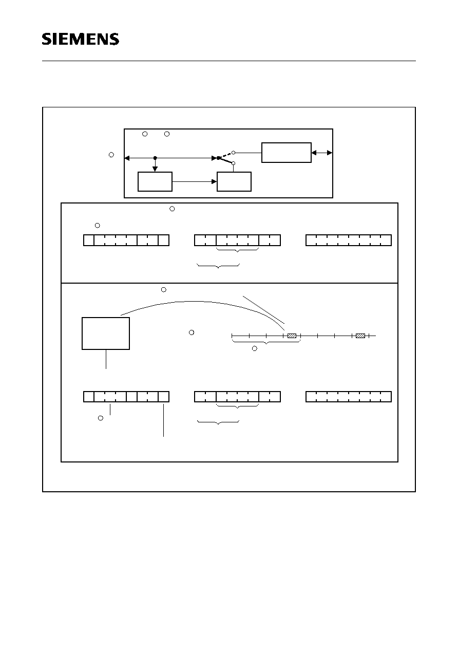
PEB 2055
PEF 2055
Appendix
Semiconductor Group
265
8.1.5
Receiving and Transmitting IOM
ģ
-2 C/I-Codes
Figure 104
Receiving and Transmitting IOM
ģ
-2 C/I-Codes (working sheet)
ITD08113
0
.
.
.
1
.
.
0
MAAR
Port
IOM -2 Channel
R
MADR
1
1
.
.
.
.
.
.
C/I Value (W)
Write Command
0
1 0 0
1 0 0 0
MACR
1 1
4 Bit C/I
6 Bit C/I Value
Transmitting a C/I Code on IOM -2 Data Downstream:
Receiving a C/I Code on IOM -2 Data Upstream:
C/I-FIFO
1. ...
2. ...
3. ...
IOM -2 Frame
R
B1
B2
M
C/I
B1
B2
M
C/I
R
IOM -2 Channel
C/I change detected
Interrupt : ISTA : SFI
Read CFIFO and copy value to MAAR
6 Bit C/I Value
4 Bit C/I Value
MACR
0
0
0
1
0
0
1
1
Read Command
C/I Value (R)
.
.
.
.
.
.
1 1
MADR
C/I FIFO
Port
MAAR
.
.
1
.
.
.
1
C/I
D
R
IOM -2
CFI Mode 0
R
EPIC
R
ELIC,
PCM TS
Data Memory
Pointer
CM Data
C/I-FIFO
R
R
IOM -2 Channel
R
4 Bit C/I Value : 0
6 Bit C/I Value : 1

PEB 2055
PEF 2055
Appendix
Semiconductor Group
266
8.2
Development Tools
The SIPB 5000 system can be used as a platform for all development steps. In a later
stage it is of course necessary to make a cost optimized design. For this, a subset of the
board design can be used. All the wiring diagrams are shipped with the board to speed
up this process.
Siemens offers a very convenient menu driven testing and debugging software. The
package that is delivered with the user board, allows a direct access to the chip registers
using symbolic names. Subsequent access may be written to a file and run as a track
file. Example track files are delivered in the package and will be a great help to the user.
8.2.1
SIPB 5000 Mainboard
Figure 105
SIPB_5000 Mainboard
The SIPB 5000 Mainboard is the general backbone of the SIPB 5XXX user board
system. It is designed as a standard PC interface card, and it contains basically a
80C188 CPU system with 7 interfaces. The interface to the PC is realized both as a Dual
Port Ram and as an additional DMA interface. Up to three daughter modules (see dotted
blocks) can be added to the Mainboard. They typically carry the components under
evaluation. The interfaces which are accessible from the back side of the PC have a
connection to the daughter modules as well. This is to allow access to the components
under evaluation while the complete board system is hidden inside the PC.
Description
Part Number
Ordering Code
SIPB Mainboard
SIPB 5000
Q67100-H8647
ITB05758
System
80C188 CPU
SAC 1
SAC 2
SAC 3
AMC 3
AMC 2
RAM
Interface
AMC 1
Dual Port
PC
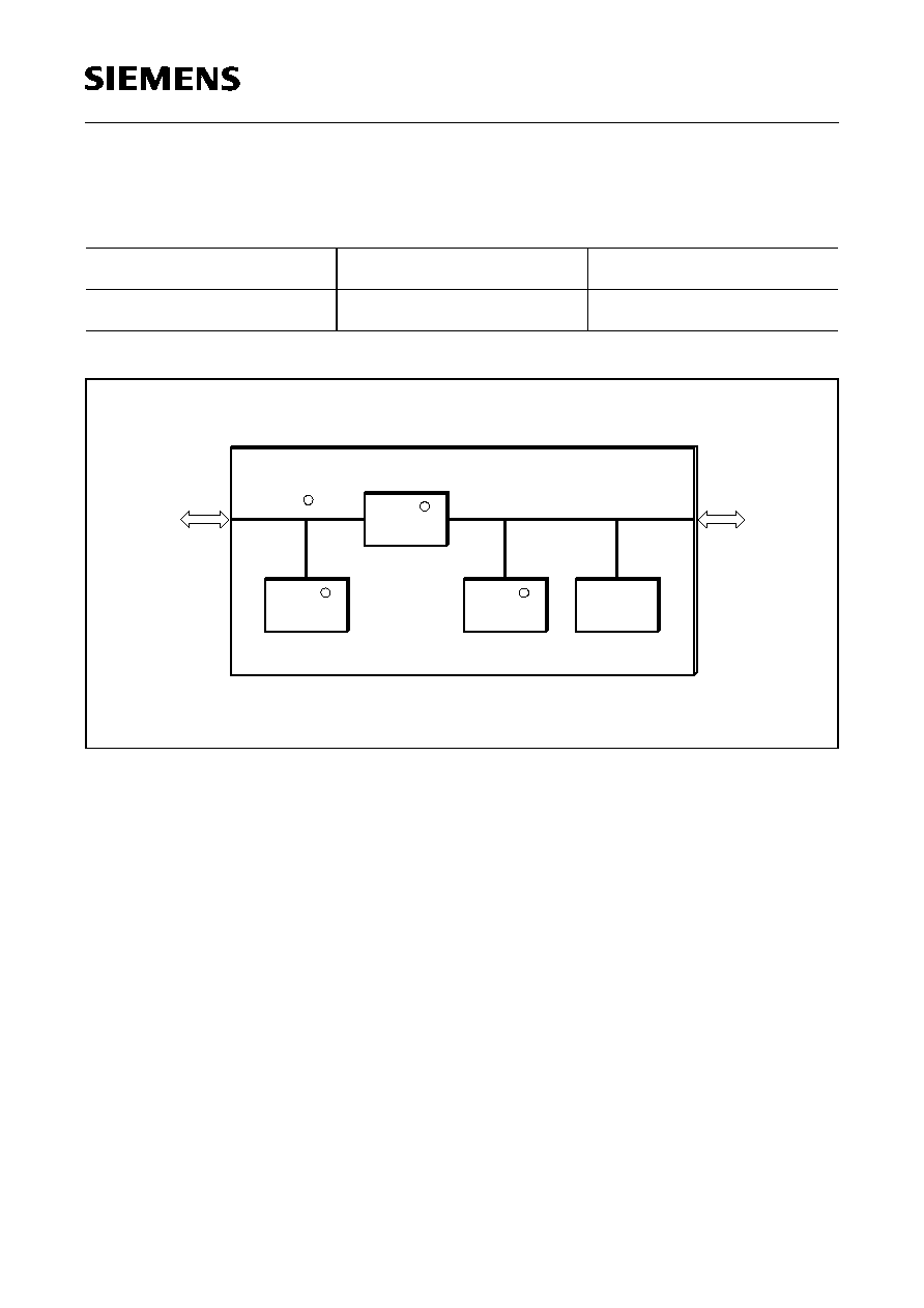
PEB 2055
PEF 2055
Appendix
Semiconductor Group
267
8.2.2
SIPB 5121 IOM
ģ
-2 Line Card (EPIC
ģ
/IDEC
ģ
)
Figure 106
SIPB 5121 IOM
ģ
-2 Line Card (EPIC
ģ
/IDEC
ģ
)
The Line Card Module SIBP 5121 is designed to be used with the ISDN User Board
SIPB 5000. It serves as an evaluation tool for various line card architectures using the
Enhanced PCM Interface Controller EPIC PEB 2055.
Some possible applications are e.g.:
≠ Centralized / decentralized D-channel handling of signaling and packet data
≠ Emulation of a PABX with primary rate module SIPB 7200
≠ Emulation of a small PABX using two line cards
≠ Emulation of a digital or analog line card using appropriate layer-1 and/or CODEC
filter modules
Description
Part Number
Ordering Code
IOM-2 Line Card Module
SIPB 5121
Q67100-H8656
ITB05759
EPIC
PEB 2055
AMC
SAC
AMC
2075
PEB
IDEC
2075
PEB
IDEC
HSCX
SAB 82525
PCM
SLD / IOM /PCM
R
R
R
R

PEB 2055
PEF 2055
Appendix
Semiconductor Group
268
8.2.3
EPIC
ģ
Configurator
Figure 107
EPIC
ģ
Configuration Tool: Screen Shot
The EPIC Configurator is an expert system which helps to initialize the IOM-2
controllers:
∑ PEB 2015 (MICO)
∑ PEB 2054 (EPIC-S)
∑ PEB 2055 (EPIC-1)
∑ PEB 2055 (ELIC) (only functional units: EPIC, SACCO-A + arbiter)
A menu driven software allows the user to define the system requirements on a
functional level.
The Configurator then generates a programming sequence in C code for initializing the
EPIC, providing all required register values.

PEB 2055
PEF 2055
Lists
Semiconductor Group
269
9
Lists
9.1
Glossary
ARCOFI
ģ
Audio ringing codec filter
BPF
Bits per PCM frame
CFI
Configurable interface
CM
Control memory
CO
Central office
DCL
Data clock
EPIC
ģ
Extended PCM interface controller
ETSI
European telecommunication standards institute
FIFO
First-in first-out (memory)
FSC
Frame synchronisation clock
HDLC
High-level data link control
IC
Integrated circuit
ID
Identifier
IOM
ģ
ISDN oriented modular
ISAC
ģ
-P
ISDN subscriber access controller on U-interface
OCTAT
ģ
-P Octal transceiver for U
PN
-interfaces
PBC
Peripheral bus controller
PBX
Private branch exchange
PCM
Pulse code modulation
PDC
PCM interface data clock
PFS
PCM interface frame synchronisation
TE
Terminal equipment
U
PN
U-interface in private network (PBX)