 | –≠–ª–µ–∫—Ç—Ä–æ–Ω–Ω—ã–π –∫–æ–º–ø–æ–Ω–µ–Ω—Ç: PT4800 | –°–∫–∞—á–∞—Ç—å:  PDF PDF  ZIP ZIP |
PT4800/PT4800F/PT4810/PT4810F/PT4850F
PT4800/PT4800F/PT4810
PT4810F/PT4850F
s Absolute Maximum Ratings
( Ta = 25∞C)
s
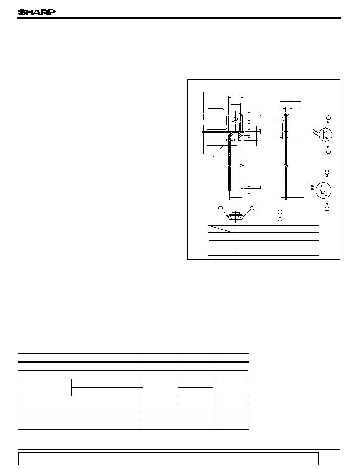
Outline Dimensions
*1 For 3 seconds at the position of 1.8mm from the bottom face of resin package
Thin Type Phototransistor
s
Features
s
Applications
PT4800F/PT4810F/PT4850F
PT4800/PT4800F/PT4850F
PT4810/PT4810F
4. Thin type
2. Floppy disk drives
1
2
1
2
2
1
1.5
0.8
2
-
0.25
0.7
PT4810/F
2.54
1.0
3.5
1.7
1.8
0.8
0.8
2
-
0.45
1. VCRs
PT4800/F
PT4850F
2
-
0.9
Rest of gate
2
-
C0.5
g
Epoxy resin
3.0
1.6
PT4810F
Mark(blue)
PT4850F
Mark(black)
1 Emitter
2 Collector
PT4800
PT4810
F type
data books, etc. Contact SHARP in order to obtain the latest version of the device specification sheets before using any SHARP's device.
"
"
In the absence of confirmation by device specification sheets, SHARP takes no responsibility for any defects that occur in equipment using any of SHARP's devices, shown in catalogs,
1. Thin type package ( Thickness : 1.5mm )
2. Visible light cut-off type :
3. Single phototransistor output :
Darlington phototransistor output:
( Unit : mm)
g
Epoxy resin
Transparent resin
Transparent blue resin
Visible light cut-off resin (black )
Parameter
Symbol
Rating
Unit
Collector-emitter voltage
V
CEO
35
V
Emitter-collector voltage
V
ECO
6
V
Collector current
PT4800/PT4800F/PT4850F
I
C
20
mA
PT4810/PT4810F
50
Collector power dissipation
P
C
75
mW
Operating temperature
T
opr
- 25 to + 85
∞C
Storage temperature
T
stg
- 40 to + 85
∞C
*1
Soldering temperature
T
sol
260
∞C
:
0.3
MAX
Burry's dimensions
:
0.3
MAX
17.5
±
0.5
0.5
MIN.
0.8
PT4800/PT4800F/PT4810/PT4810F/PT4850F
s
Electro-optical Characteristics
*2 E
e
: Irradiance by CIE standard light source A ( tungsten lamp)
Parameter
Symbol
Conditions
MIN.
TYP.
MAX.
Unit
*2
Collector current
PT4800
I
C
E
e
= 1mW/cm
2
V
CE
= 5V
0.12
0.4
1.0
mA
PT4800F
0.08
0.25
0.75
mA
PT4850F
0.12
-
0.56
mA
PT4810
E
e
= 0.1mW/cm
2
0.45
-
7.0
mA
PT4810F
0.27
-
6.0
mA
V
CE
= 2V
Collector dark current
PT4800/PT4800F
I
CEO
E
e
= 0, V
CE
= 20V
-
-
0.1
m A
PT4850F
PT4810/PT4810F
E
e
= 0, V
CE
= 10V
-
-
1.0
m A
voltage
PT4800/PT4800F
V
CE
(sat)
E
e
= 10mW/cm
2
-
-
0.4
V
PT4850F
I
C
= 0.5mA
PT4810/PT4810F
E
e
= 1mW/cm
2
-
-
1.0
V
I
C
= 2.5mA
Collector-emitter breakdown voltage
BV
CEO
I
C
= 0.1mA
35
-
-
V
E
e
= 0
Emitter-collector breakdown voltage
BV
ECO
I
E
= 0.01mA
6
-
-
V
E
e
= 0
Peak sensitivity
wavelength
PT4800
p
-
800
-
nm
PT4800F
-
860
-
nm
PT4850F
-
-
860
-
nm
PT4810
-
800
-
nm
PT4810F
-
860
-
nm
t
r
V
CE
= 2V, I
C
= 2mA
-
3.0
-
µ
s
R
L
= 100
V
CE
= 2V
I
C
= 10mA
R
L
= 100
-
80
400
µ
s
t
f
V
CE
= 2V, I
C
= 2mA
-
3.5
-
µ
s
R
L
= 100
V
CE
= 2V
I
C
= 10mA
R
L
= 100
-
70
350
µ
s
Half intensity angle
-
-
± 35
-
PT4800/PT4800F
PT4850F
PT4810/PT4810F
PT4800/PT4800F
PT4850F
PT4810/PT4810F
*2
Collector-emitter saturation
( Ta = 25∞C)
- 25
0
25
50
75
100
0
20
40
60
80
100
85
0
25
50
75
100
2
5
2
5
2
5
2
5
Collector power dissipation P
C
(
mW
)
Ambient temperature T
a
(∞C)
Ambient temperature T
a
(∞C)
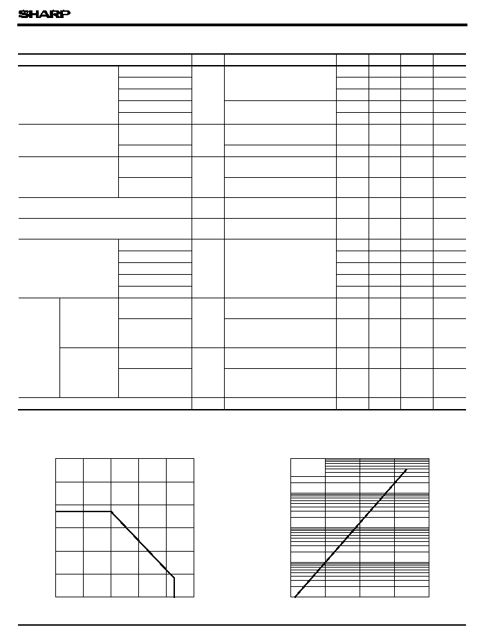
Fig. 1 Collector Power Dissipation vs.
Ambient Temperature
Collector dark current I
CEO
(
A
)
(PT4800/PT4800F/PT4850F )
Response
time
Rise time
Fall time
Fig. 2-a Collector Dark Current vs.
Ambient Temperature
V
CE
= 20V
10
- 6
10
- 7
10
- 8
10
- 9
10
- 10
∞
PT4800/PT4800F/PT4810/PT4810F/PT4850F
Ambient temperature T
a
(∞C)
- 25
0
25
50
75
100
10
- 11
5
10
- 10
5
10
- 9
5
10
- 8
5
10
- 7
5
10
- 6
5
10
- 5
5
10
- 4
5
= 10V
40
0
0
20
10
20
30
40
70
50
60
160
100
60
80
120
140
Ambient temperature T
a
(∞C)
Relative collector current
(
%
)
150
125
100
75
50
- 25
Relative collector current
(
%
)
50
0
25
75
100
Collector current I
C
(
mA
)
1
10
1
10
0.1
0.2
0.5
2
5
20
0.1
0.2
0.5
2
5
20
Collector current I
C
(
mA
)
1
10
0.1
1
0.1
0.2
0.5
2
5
20
0.05
0.2
0.5
2
5
10
Collector current I
C
(
mA
)
1
2
5
2
5
0.1
0.2
0.5
2
5
PT4810
PT4810F
(PT4800/PT4800F/PT4850F )
Collector dark current I
CEO
(
A
)
Ambient temperature T
a
(∞C)
( PT4810/PT4810F )
( PT4810/PT4810F )
( PT4810/PT4810F )
(PT4800 )
( PT4800F/PT4850F )
Irradiance E
e
( mW/cm
2
)
Irradiance E
e
( mW/cm
2
)
Irradiance E
e
( mW/cm
2
)
Fig. 2-b Collector Dark Current vs. Ambient
Temperature
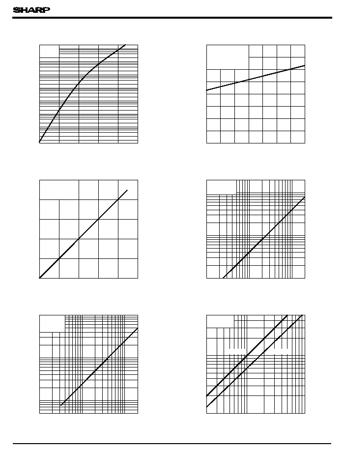
Fig. 3-a Relative Collector Current vs.
Ambient Temperature
Fig. 4-a Collector Current vs.
Irradiance
Fig. 3-b Relative Collector Current vs.
Ambient Temperature
Fig. 4-b Collector Current vs. Irradiance
Fig. 4-c Collector Current vs. Irradiance
V
CE
E
e
= 1mW/cm
2
V
CE
= 5V
V
CE
= 5V
T
a
= 25∞C
E
e
= 0.1mW/cm
2
V
CE
= 2V
V
CE
= 5V
T
a
= 25∞C
V
CE
= 2V
T
a
= 25∞C
10
-1
175
1

PT4800/PT4800F/PT4810/PT4810F/PT4850F
Collector-emitter voltage V
CE
(V)
Collector current I
C
(
mA
)
0
5
10
15
20
25
30
35
0
0.1
0.2
0.3
0.4
0.5
0.6
Collector-emitter voltage V
CE
(V)
Collector current I
C
(
mA
)
0
2
4
6
8
10
12
14
0
0.2
0.4
0.6
0.8
1.0
1.2
Collector current I
C
(
mA
)
0
1
2
3
4
5
6
0
0.4
0.8
1.2
1.6
2.0
2.4
Collector current I
C
(
mA
)
0
1
2
3
4
5
6
0
0.2
0.4
0.6
0.8
1.0
1.2
Wavelength
( nm )
Relative sensitivity
(
%
)
400
500
600
700
800
900
0
20
40
60
80
100
PT4800
PT4810 PT4800F
PT4801F
PT4850F
1
10
0.1
0.2
0.5
2
5
10
1
2
5
20
50
100
Collector-emitter voltage V
CE
(V)
Collector-emitter voltage V
CE
(V)
)
(PT4800 )
(PT4800F/PT4850F )
(PT4810 )
(PT4810F )
Response time t
r
, t
f
(
µ
s
)
Fig. 5-a Collector Current vs.
Collector-emitter Voltage
0.1mW/cm
2
Fig. 5-b Collector Current vs.
Collector-emitter Voltage
Fig. 5-c Collector Current vs.
Collector-emitter Voltage
Fig. 6 Spectral Sensitivity
Fig. 5-d Collector Current vs.
Collector-emitter Voltage
T
a
= 25∞C
E
e
= 1.0mW/cm
2
0.75mW/cm
2
0.5mW/cm
2
0.25mW/cm
2
T
a
= 25∞C
E
e
= 3mW/cm
2
2.5mW/cm
2
2.0mW/cm
2
1.5mW/ cm
2
1.0mW/cm
2
0.8mW/cm
2
0.6mW/cm
2
T
a
= 25∞C
E
e
= 0.2mW/cm
2
0.15mW/cm
2
0.1mW/cm
2
0.08mW/cm
2
0.06mW/cm
2
0.04mW/cm
2
0.02mW/cm
2
T
a
= 25∞C
E
e
= 0.2mW/cm
2
0.15mW/cm
2
0.1mW/cm
2
0.08mW/cm
2
0.06mW/cm
2
0.04mW/cm
2
0.02mW/cm
2
T
a
= 25∞C
1100
1000
V
CE
= 2V
I
C
= 2mA
T
a
= 25∞C
t
f
t
r
t
r
t
f
PT4800/PT4800F/PT4850F
(
Fig. 7-a Response Time vs. Load Resistance
Load resistance R
L
( k
)

L
(
)
Response time
(
µ
s
)
10
100
10
100
1
t
r
Output
Test Circuit for Response Time
V
CC
R
L
Output Input
10
%
t
f
90
%
Angular displacement
0
Test Circuit for Response Time
t
d
t
r
Output
V
CC
Output
R
L
Input
t
f
10
%
t
s
90
%
1
0
0.2
0.4
0.6
0.8
1.0
1.2
1.4
1.6
1.8
2.0
2.2
0.1
0.2
0.5
2
5
10
0.1mA
0.5mA
1.0mA
1.5mA
1
10
0
0.2
0.4
0.6
0.8
1.0
1.2
1.4
1.6
1.8
2.0
2.2
0.1
0.2
0.5
2
5
20
0.1mA
0.5mA
1.0mA
2.0mA
1.5mA
( T
a
= 25∞C)
- 80∞
- 90∞
- 60∞
- 70∞
- 50∞
- 40∞
- 30∞
Relative sensitivity
(%
)
+ 80∞
+ 90∞
+ 10∞
80
20
40
60
- 10∞
- 20∞
0∞
100
+ 70∞
+ 60∞
+ 50∞
+ 40∞
+ 20∞
+ 30∞
(PT4800 )
(PT4800F/ PT4850F)
( PT4810 / PT4810F)
( PT4800 / PT4800F/ PT4850F)
( PT4810 / PT4810F)
PT4800/PT4800F/PT4810/PT4810F/PT4850F
Irradiance E
e
( mW/cm
2
)
Irradiance E
e
( mW/cm
2
)
Collector-emitter saturation voltage
V
CE
( sat
)
Collector-emitter saturation voltage
V
CE
( sat
)
(
V
)
Fig. 8 Sensitivity Diagram
Fig. 9-a Collector-emitter Saturation
Voltage vs. Irradiance
Fig. 9-b Collector-emitter Saturation
Voltage vs. Irradiance
V
CE
= 2V
I
C
= 10mA
T
a
= 25∞C
t
r
t
f
t
d
t
s
T
a
= 25∞C
I
C
=
0.05mA
T
a
= 25∞C
I
C
=
0.05mA
1000
1000
5000
Fig. 7-b Response Time vs. Load Resistance
Load resistance R