Overview
The LC378000RP is an 8-Mbit mask ROM that can be
switched between byte mode, which provides an 8-bit
◊
1,048,576-word structure, and word mode, which provides
a 16-bit
◊
524,288-word structure. Since this device
operates over the wide supply voltage range of 2.6 to
5.5 V and achieves access times (t
AA
) of 100 ns (at V
CC
=
4.5 to 5.5 V) and 200 ns (at V
CC
= 2.6 to 5.5 V), it can be
used in a wide range of systems, from 5-V systems
requiring high-speed access to 3-V battery operated
systems.
Features
∑ Supply voltage range: 2.6 to 5.5 V
∑ Access time (t
AA
): 100 ns (V
CC
= 4.5 to 5.5 V)
(t
CA
): 110 ns (V
CC
= 4.5 to 5.5 V)
200 ns (V
CC
= 2.6 to 5.5 V)
∑ Switchable between 8-bit and 16-bit data path widths
Byte mode: 1,048,576 words
◊
8 bits
Word mode: 524,288 words
◊
16 bits
∑ Operating current drain: 90 mA (maximum)
∑ Standby current: 30 µA (maximum)
∑ Fully static operation (internal synchronization)
∑ Three-state outputs
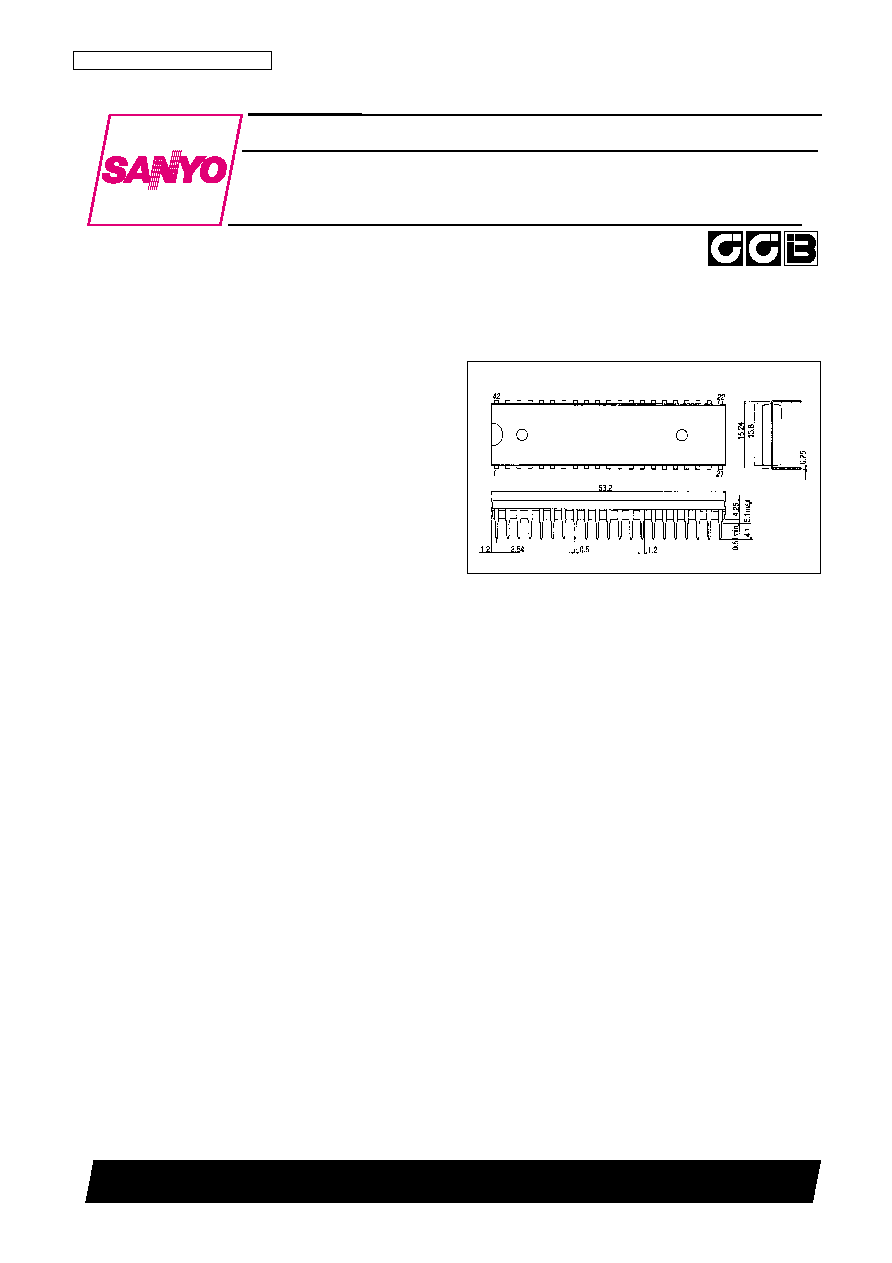
∑ Package: 42-pin DIP (600 mil) plastic package
Package Dimensions
unit: mm
3014A-DIP42
CMOS IC
42098RM (OT) No. 5793-1/4
Preliminary
SANYO: DIP42
[LC378000RP]
SANYO Electric Co.,Ltd. Semiconductor Bussiness Headquarters
TOKYO OFFICE Tokyo Bldg., 1-10, 1 Chome, Ueno, Taito-ku, TOKYO, 110-8534 JAPAN
Internally Synchronized Silicon Gate 8M (1,048,576-
word
◊
8-bit, 524,288-word
◊
16-bit) Mask ROM
LC378000RP
Ordering number : EN
*
5793

Pin Assignment
No. 5793-2/4
LC378000RP
Block Diagram
Pin Functions
D15/A-1:In byte mode, this pin functions as
the A-1 address input, and in word
mode, it functions as the D15 data
output pin.
A0 to A19
Address inputs
D0 to D15/A-1
Data outputs
CE
Chip enable input
OE
Output enable input
BYTE
Byte/word mode switching
V
CC
Power
V
SS
Ground
Function Logic Table
Note: X: A high-level or low-level input
D8 to 14 are high impedance and D15 functions as the A-1 address input.
CE
OE
BYTE
Output pin state
Current drain
H
X
L
High impedance
Standby mode level
L
H
L
High impedance
Operating mode level
L
L
L
DOUT
◊
8 (BYTE MODE)
*
Operating mode level
H
X
H
High impedance
Standby mode level
L
H
H
High impedance
Operating mode level
L
L
H
DOUT
◊
16 (WORD MODE)
Operating mode level
Address buffer
Row decoder
Memory array
Column decoder
+ bias circuit
Sense amplifier
Byte/word output
switching circuit
Output buffer
A-1 buffer
CE buffer
BYTE buffer
OE buffer
Internal timing
generator

No. 5793-3/4
LC378000RP
Parameter
Symbol
Conditions
Ratings
Unit
Supply voltage
V
CC
≠0.3 to +7.0
V
Input pin voltage
V
IN
≠0.3
*
to V
CC
+ 0.3
V
Output pin voltage
V
OUT
≠0.3 to V
CC
+ 0.3
V
Allowable power dissipation
Pd max
Ta = 25∞C
1.0
W
Operating temperature
Topr
≠10 to +70
∞C
Storage temperature
Tstg
≠55 to +125
∞C
Note: Application of stresses greater than or equal to the maximum ratings may lead to device destruction.
*
: Minimum value minus 3.0 V for pulses with widths of 30 ns or less.
Note: These parameters are not tested in all units, but rather are sampled in a subset of units produced.
Note: Values in parentheses are guaranteed at Ta = 25∞C.
Note: t
OD
is stipulated as the time from the rise of either CE or OE (whichever occurs first) to the point when the output goes to the high-impedance state.
These parameters are not tested in all units, but rather are sampled in a subset of units produced.
Values in parentheses are for V
CC
= 4.5 to 5.5 V.
Specifications
Absolute Maximum Ratings
*
Parameter
Symbol
Conditions
Ratings
Unit
min
typ
max
Input pin capacitance
C
IN
V
IN
= 0 V. Reference value using the Sanyo DIP.
8
pF
Output pin capacitance
C
OUT
V
OUT
= 0 V. Reference value using the Sanyo DIP.
10
pF
Capacitance Characteristics
* at Ta = 25∞C, f = 1.0 MHz
Parameter
Symbol
Conditions
Ratings
Unit
min
typ
max
Supply voltage
V
CC
max
2.6
5.0
5.5
V
Input high-level voltage
V
IH
2.2
V
CC
+ 0.3
V
Input low-level voltage
V
IL
≠0.3
0.6
V
DC Allowable Operating Ranges
at Ta = ≠10 to +70∞C
Parameter
Symbol
Conditions
Ratings
Unit
min
typ
max
Operating current drain
I
CCA1
CE = 0.2 V, V
I
= V
CC
≠ 0.2 V/0.2 V
30
mA
I
CCA2
CE = V
IL
, I
O
= 0 mA, V
I
= V
IH
/V
IL
, f = 10 MHz
90
mA
Standby current drain
I
CCS1
CE = V
CC
≠ 0.2 V
30 (1.0)
µA
I
CCS2
CE = V
IH
1.0 (0.3)
mA
Input leakage current
I
LI
V
IN
= 0 to V
CC
±1.0
µA
Output leakage current
I
LO
CE or OE = V
IH
, V
OUT
= 0 to V
CC
±1.0
µA
Output high-level voltage
V
OH
I
OH
= ≠0.5 mA
0.8 V
CC
V
Output low-level voltage
V
OL
I
OL
= 0.5 mA
0.2
V
DC Electrical Characteristics
at Ta = ≠10 to +70∞C, V
CC
= 2.6 to 5.5 V
Parameter
Symbol
Conditions
Ratings
Unit
min
typ
max
Cycle time
t
CYC
200 (100)
ns
Address access time
t
AA
200 (100)
ns
CE enable time
t
CEON
200 (135)
ns
CE access time
t
CA
200 (110)
ns
OE access time
t
OA
100 (40)
ns
Output hold time
t
OH
20
ns
Output disable time
*
t
OD
100
ns
AC Characteristics
at Ta = ≠10 to +70∞C, V
CC
= 2.6 to 5.5 V

PS No. 5793-4/4
LC378000RP
This catalog provides information as of April, 1998. Specifications and information herein are subject to change
without notice.
s
No products described or contained herein are intended for use in surgical implants, life-support systems, aerospace
equipment, nuclear power control systems, vehicles, disaster/crime-prevention equipment and the like, the failure of
which may directly or indirectly cause injury, death or property loss.
s
Anyone purchasing any products described or contained herein for an above-mentioned use shall:
Accept full responsibility and indemnify and defend SANYO ELECTRIC CO., LTD., its affiliates, subsidiaries and
distributors and all their officers and employees, jointly and severally, against any and all claims and litigation and all
damages, cost and expenses associated with such use:
Not impose any responsibility for any fault or negligence which may be cited in any such claim or litigation on
SANYO ELECTRIC CO., LTD., its affiliates, subsidiaries and distributors or any of their officers and employees
jointly or severally.
s
Information (including circuit diagrams and circuit parameters) herein is for example only; it is not guaranteed for
volume production. SANYO believes information herein is accurate and reliable, but no guarantees are made or implied
regarding its use or any infringements of intellectual property rights or other rights of third parties.
Test Conditions
Timing Waveforms
Output Load
Input voltage amplitude
0.4 V to 2.8 V
Rise and fall times
5 ns
Input discrimination level
1.5 V
Output discrimination level
1.5 V
Output load
See figure.
*
: Includes the oscilloscope and
jig capacitances.
Note: Items in parentheses are for byte mode operation.
Notes on System Design
This IC adopts the ATD technique, in which operation starts when a change in either the CE or address inputs is detected.
This means that the output data immediately after power is applied is invalid. When using this IC as program memory for
the Z80 and similar microprocessors, applications must take into account the fact that valid data will not be output after
power is first applied unless the value of either the CE line or at least one of the address lines is changed after the power
supply has stabilized.
Another point due to the use of the ATD technique is that this IC is sensitive to input noise. Do not apply voltages
outside the allowable DC input levels for extended periods and do not apply input voltages with large noise components.
Address input
Data output
t
CEON