
144 RGB Segment & 177 Common Driver For 65,536 Color STN LCD
August. 12. 2002
Ver. 1.1
S6B33B0A
Contents in this document are subject to change without notice. No part of this document may be reproduced or
transmitted in any form or by any means, electronic or mechanical, for any purpose, without the express written
permission of LCD Driver IC Team.
Precautions for Light
Light has characteristics to move electrons in the integrated circuitry of semiconductors, therefore may change
the characteristics of semiconductor devices when irradiated with light. Consequently, the users of the
packages which may expose chips to external light such as COB, COG, TCP and COF must consider effective
methods to block out light from reaching the IC on all parts of the surface area, the top, bottom and the sides
of the chip. Follow the precautions below when using the products.
1. Consider and verify the protection of penetrating light to the IC at substrate (board or glass) or product
design stage.
2. Always test and inspect products under the environment with no penetration of light.

144 RGB SEGMENT & 177 COMMON DRIVER FOR 65,536 COLOR STN LCD S6B33B0A PRELIMINARY VER 1.1
2
S6B33B0A Specification Revision History
Version
Content
Date
0.0
Original
Neglect the more past version than version 0.0
Mar. 2002
0.1
Add the schottky barrier diode connection between VEE and VSS
at the system application diagram
May. 2002
0.2
Append the schottky barrier diode specification
Append the addressing condition for the 256 color and 4.096 color mode
June. 2002
0.3
Append the power on/off sequences.
June. 2002
1.0
Definition of TBD items
July. 2002
1.1
Modify REG_OUT range: 1.8 to 1.9V -> 1.8 to 2.2V
Add the DC spec for VIN2, DC2IN, VIN45.
Aug. 2002

S6B33B0A PRELIMINARY VER 1.1 144 RGB SEGMENT & 177 COMMON DRIVER FOR 65,536 COLOR STN LCD
3
CONTENTS
INTRODUCTION ............................................................................................................................................ 1
FEATURES .................................................................................................................................................... 1
BLOCK DIAGRAM ......................................................................................................................................... 2
PAD CONFIGURATION ................................................................................................................................. 3
PIN CONFIGURATION................................................................................................................................... 5
PAD CENTER COORDINATES ...................................................................................................................... 6
PIN DESCRIPTION .......................................................................................................................................11
PIN DESCRIPTION .......................................................................................................................................12
FUNCTIONAL DESCRIPTION .......................................................................................................................15
MPU INTERFACE ..................................................................................................................................15
DISPLAY DATA RAM .............................................................................................................................19
INSTRUCTION DESCRIPTION ......................................................................................................................28
INSTRUCTION PARAMETER ........................................................................................................................56
POWER ON/OFF SEQENCE .........................................................................................................................59
SPECIFICATIONS .........................................................................................................................................61
ABSOLUTE MAXIMUM RATINGS ...........................................................................................................61
OPERATING VOLTAGE .........................................................................................................................61
DC CHARACTERISTICS (1) ...................................................................................................................62
DC CHARACTERISTICS (2) ...................................................................................................................63
DC CHARACTERISTICS (3) ...................................................................................................................64
DC CHARACTERISTICS (4) ...................................................................................................................65
DC CHARACTERISTICS (5) ...................................................................................................................66
AC CHARACTERISTICS .........................................................................................................................67
SYSTEM APPLICATION DIAGRAM ...............................................................................................................71


S6B33B0A PRELIMINARY VER 1.1 144 RGB SEGMENT & 177 COMMON DRIVER FOR 65,536 COLOR STN LCD
1
INTRODUCTION
S6B33B0A is a mid-display-size-compatible driver for liquid crystal dot matrix gray-scale graphic systems. With on-
chip CR oscillator circuit, the display-timing signal is generated without being sent from MPU. Also, it is capable of
using 8bit/16bit data bus alternatively and operating with 68/80-series MPU in asynchronous. Due to the LCD
driving signal (144 RGB X 177 output) corresponding to the display data and the internal bit-map display RAM of
144
�
176
�
16-bit, S6B33B0A is capable of operating max. 144 RGB x 177 dot LCD panels in low-power
consumption. Being the segment RGB 3-output, one pixel is 16-bit data and S6B33B0A can max display 65,536
color.
FEATURES
Driver Output
-
144 RGB x 177
Gray Scale Function
-
65,536 color display of R: 32 gray scale, G: 64 gray scale, B: 32 gray scale
-
4,096 color display of R: 16 gray scale, G: 16 gray scale, B: 16 gray scale
-
256 color display of R: 8 gray scale, G: 8 gray scale, B: 4 gray scale
On-chip Display Data RAM
-
Capacity: 144 x 16 x 176 = 405.504k bits
-
Burst RAM write function
Display Mode
-
Normal display mode: Entire duty displaying
-
Partial display mode: Partial duty displaying
-
Standby mode: Internal display clocks off
-
Area scroll mode: Particular area scrolling
Microprocessor Interface
-
8-bit/16 bit parallel bi-directional interface with 6800-series or 8080-series
-
3/4 Pin SPI (only write operation)
On-chip Low Power Analog Circuit
-
On-chip CR oscillator (Internal cap. & external resistor), external clock available
-
Voltage converter / Voltage regulator / Voltage follower
-
On-chip electronic contrast control (256 steps)
Operating Voltage Range
-
VDD
:
1.8 to 3.3 [V] (without Internal Regulator), 2.4 to 3.3 [V] (With internal Regulator)
-
VIN1: 2.4 to 3.6 [V]
-
Display operating voltage(V1): 2.0 to 4.0 V
-
LCD Operating Voltage Range : Max. 20 V
Low Power Consumption
-
650
�
A Typ. (Refer to DC CHARACTERISTICS (2))
Package Type
-
COG (Output Pad Pitch Min. 40
�
m)

144 RGB SEGMENT & 177 COMMON DRIVER FOR 65,536 COLOR STN LCD S6B33B0A PRELIMINARY VER 1.1
2
BLOCK DIAGRAM
COM
Driving Circuit
LCD
System
Control
Circuit
Bus
Holder
MPU INTERFACE
CS2
CS1B
DB<15:0>
Display data RAM
176 X 2304
MPU System
Control Circuit
Instruction Decoder
SEG
Driving Circuit
Y - Address
Control
Circuit
I/O Buffer
X - Address
Control
Circuit
Status
Oscillator
Circuit
Voltage
Converter/
Voltage
Regulator/
Voltage
Follower
PS
RSTB
VRN
VMIN
VRP
V1IN
REG_ENB
REG_OUT
Power
Regulator
Circuit
Decoder Circuit
2304
432
176
PM
FR
CL
VSS
VEE
VCC
VIN2
VIN45
VOUT45
C11P
C11M
C12M
C12P
VIN1
V1T
C21P
C22M
C22P
C21M
C23P
C23M
C24P
C24M
C31P
C31M
INTRS
VDD3, VDD3R
VDD,VDDO
V0IN
VMOUT
V1OUT
OSC5
OSC2
OSC3
OSC4
OSC1
SEGA0
SEGB0 - - -
SEGC0
COM0 - - - COM176
SEGA143
SEGB143
SEGC143
DC2OUT
DC2IN
MPU[1:0]
WRB
D/I(RS)
RDB
CDIR
VSS,VSSA,VSSB,VSSO
Figure 1. Block Diagram

S6B33B0A PRELIMINARY VER 1.1 144 RGB SEGMENT & 177 COMMON DRIVER FOR 65,536 COLOR STN LCD
3
PAD CONFIGURATION
.......................
..
............
.
X
Y
(0,0) S6B33B0
PAD
777
1
219
279
220
278
836
778
TOM
ALIGN KEY
Figure 2. S6B33B0A Chip Pad Configuration
Table 1. S6B33B0A Pad Dimensions
Size
Item
Pad No.
X
Y
Unit
Chip size
(with S/L 120
�
m)
20644
2870
1 to 219
90
Pad pitch
220 to 278, 279 to 777, 778 to 836
40
1 to 219
70
70
220 to 278, , 778 to 836
150
25
Bumped
pad size
279 to 777
25
150
Bumped pad height
All pad
17
�
m

144 RGB SEGMENT & 177 COMMON DRIVER FOR 65,536 COLOR STN LCD S6B33B0A PRELIMINARY VER 1.1
4
COG Align Key Coordinate ILB Align Key Coordinate
30
�
m 30
�
m 30
�
m
30
�
m 30
�
m 30
�
m
30
�
m
30
�
m
30
�
m
60
�
m
30
�
m
42
�
m
108
�
m
42
�
m
108
�
m
42
�
m
108
�
m
42
�
m
108
�
m
(-8100,780)
(8618,-855)
(-8270,-928)
(8670,820)
Figure 3. COG Align Key Coordinate
Figure 4. ILB Align Key Coordinate
TOM(TEG On Main chip) Coordinate
COF Align Key Coordinate
220um
(
-
8270
,
-
40)
(
-
8050
,
540
)
58
0u
m
(
-
8000
,
-
670
)
(
-
7780
,
-
90
)
58
0u
m
220um
(
-
8000
,
-
40)
(
-
7780
,
540
)
70um
70um
70
um
(-10085,1268)
(-10155,1198)
(10155,1268)
(10085,1198)
50um
20um
S6B33B0A PRELIMINARY VER 1.1 144 RGB SEGMENT & 177 COMMON DRIVER FOR 65,536 COLOR STN LCD
5
PIN CONFIGURATION
COM0
COM1
COM2
COM54
COM55
COM56
:
:
:
:
:
:
:
:
:
:
:
:
SEGC0
SEGB0
SEGA0
SEGC1
SEGB1
SEGA1
SEGC2
SEGB2
SEGA2
:
:
:
:
:
:
:
:
:
:
:
:
:
:
:
:
:
:
:
:
:
:
:
SEGC141
SEGB141
SEGA141
SEGC142
SEGB142
SEGA142
SEGC143
SEGB143
SEGA143
S6B33B0 (Top View)
C21M
C21P
DC2IN
DC2OUT
VMIN
VMOUT
V1T
V1OUT
V1IN
C12M
C12P
C11M
C11P
VOUT45
VIN45
VIN2
VIN1(VIN1A)
VDD1(VDD3=VDD3R)
REG_OUT
VDD(VDDO)
OSC1
DB15
DB14
DB13
DB12
DB11
DB10
DB9
DB8
DB7
DB6
DB5
DB4
DB3
DB2
DB1
OSC2
OSC3
OSC4
OSC5
INTRS
REG_ENB
VSS
DB0
RDB
WRB
RS
RSTB
PM
FR
CL
TEST0
TEST1
TEST2
CS2
CS1B
CDIR
MPU0
MPU1
PS
VOIN
C22M
C22P
C23M
C23P
C24M
C24P
C21M
VEE
VRM
VRP
VCC
C31M
C31P
VOIN
COM87
COM88
COM89
COM141
COM142
COM143
:
:
:
:
:
:
:
:
:
:
:
:
:
:
:
COM57
COM58
COM59
COM84
COM85
COM86
:
:
:
COM176
COM175
COM174
COM146
COM145
COM144
:
:
:
Figure 5. S6B33B0A Chip Pin Configuration

144 RGB SEGMENT & 177 COMMON DRIVER FOR 65,536 COLOR STN LCD S6B33B0A PRELIMINARY VER 1.1
6
PAD CENTER COORDINATES
Table 2. Pad Center Coordinates
[Unit:
�
m]
No
X
Y
NAME
No
X
Y
NAME
No
X
Y
NAME
1
-9808
-1320
DUMMY<0>
51
-5308
-1320
VSS
101
-808
-1320
VDD3
2
-9718
-1320
DUMMY<1>
52
-5218
-1320
VSS
102
-718
-1320
VDD3
3
-9628
-1320
V0IN
53
-5128
-1320
VSS
103
-628
-1320
VDD3
4
-9538
-1320
V0IN
54
-5038
-1320
VSS
104
-538
-1320
VDD3
5
-9448
-1320
V0IN
55
-4948
-1320
VSSA
105
-448
-1320
VDD3
6
-9358
-1320
V0IN
56
-4858
-1320
VSSA
106
-358
-1320
VIN1
7
-9268
-1320
VSS
57
-4768
-1320
VSSA
107
-268
-1320
VIN1
8
-9178
-1320
PS
58
-4678
-1320
VSSA
108
-178
-1320
VIN1
9
-9088
-1320
VDD3
59
-4588
-1320
VSSO
109
-88
-1320
VIN1
10
-8998
-1320
MPU1
60
-4498
-1320
VSSO
110
2
-1320
VIN1
11
-8908
-1320
VSS
61
-4408
-1320
VSSB
111
92
-1320
VIN1
12
-8818
-1320
MPU0
62
-4318
-1320
VSSB
112
182
-1320
VIN1
13
-8728
-1320
VDD3
63
-4228
-1320
VSSB
113
272
-1320
VIN1
14
-8638
-1320
CDIR
64
-4138
-1320
VSSB
114
362
-1320
VIN1
15
-8548
-1320
VSS
65
-4048
-1320
VSSB
115
452
-1320
VIN1
16
-8458
-1320
CS1B
66
-3958
-1320
VSSB
116
542
-1320
VIN1
17
-8368
-1320
CS2
67
-3868
-1320
VSSB
117
632
-1320
VIN1
18
-8278
-1320
TEST2
68
-3778
-1320
VSSB
118
722
-1320
VIN1A
19
-8188
-1320
TEST1
69
-3688
-1320
VSSB
119
812
-1320
VIN1A
20
-8098
-1320
TEST0
70
-3598
-1320
VSSB
120
902
-1320
VIN1A
21
-8008
-1320
VDD3
71
-3508
-1320
REG_ENB
121
992
-1320
VIN1A
22
-7918
-1320
CL
72
-3418
-1320
VDD3
122
1082
-1320
VIN2
23
-7828
-1320
FR
73
-3328
-1320
INTRS
123
1172
-1320
VIN2
24
-7738
-1320
PM
74
-3238
-1320
OSC5
124
1262
-1320
VIN2
25
-7648
-1320
RSTB
75
-3148
-1320
VSS
125
1352
-1320
VIN2
26
-7558
-1320
RS
76
-3058
-1320
OSC4
126
1442
-1320
VIN2
27
-7468
-1320
VSS
77
-2968
-1320
OSC3
127
1532
-1320
VIN45
28
-7378
-1320
WRB
78
-2878
-1320
OSC2
128
1622
-1320
VIN45
29
-7288
-1320
RDB
79
-2788
-1320
OSC1
129
1712
-1320
VIN45
30
-7198
-1320
VDD3
80
-2698
-1320
VDDO
130
1802
-1320
VOUT45
31
-7108
-1320
DB0
81
-2608
-1320
VDDO
131
1892
-1320
VOUT45
32
-7018
-1320
DB1
82
-2518
-1320
VDD
132
1982
-1320
VOUT45
33
-6928
-1320
DB2
83
-2428
-1320
VDD
133
2072
-1320
C11P
34
-6838
-1320
DB3
84
-2338
-1320
VDD
134
2162
-1320
C11P
35
-6748
-1320
DB4
85
-2248
-1320
VDD
135
2252
-1320
C11P
36
-6658
-1320
DB5
86
-2158
-1320
VDD
136
2342
-1320
C11M
37
-6568
-1320
DB6
87
-2068
-1320
VDD
137
2432
-1320
C11M
38
-6478
-1320
DB7
88
-1978
-1320
REG_OUT
138
2522
-1320
C11M
39
-6388
-1320
DB8
89
-1888
-1320
REG_OUT
139
2612
-1320
C12P
40
-6298
-1320
DB9
90
-1798
-1320
REG_OUT
140
2702
-1320
C12P
41
-6208
-1320
DB10
91
-1708
-1320
REG_OUT
141
2792
-1320
C12P
42
-6118
-1320
DB11
92
-1618
-1320
REG_OUT
142
2882
-1320
C12M
43
-6028
-1320
DB12
93
-1528
-1320
REG_OUT
143
2972
-1320
C12M
44
-5938
-1320
DB13
94
-1438
-1320
VDD3R
144
3062
-1320
C12M
45
-5848
-1320
DB14
95
-1348
-1320
VDD3R
145
3152
-1320
V1IN
46
-5758
-1320
DB15
96
-1258
-1320
VDD3R
146
3242
-1320
V1IN
47
-5668
-1320
VSS
97
-1168
-1320
VDD3R
147
3332
-1320
V1IN
48
-5578
-1320
VSS
98
-1078
-1320
VDD3R
148
3422
-1320
V1OUT
49
-5488
-1320
VSS
99
-988
-1320
VDD3R
149
3512
-1320
V1OUT
50
-5398
-1320
VSS
100
-898
-1320
VDD3
150
3602
-1320
V1OUT

S6B33B0A PRELIMINARY VER 1.1 144 RGB SEGMENT & 177 COMMON DRIVER FOR 65,536 COLOR STN LCD
7
Table 2. Pad Center Coordinates (Continued)
[Unit:
�
m]
No
X
Y
NAME
No
X
Y
NAME
No
X
Y
NAME
151
3692
-1320
V1T
201
8192
-1320
VCC
251
10120
0
COM<30>
152
3782
-1320
V1T
202
8282
-1320
VCC
252
10120
40
COM<31>
153
3872
-1320
VMOUT
203
8372
-1320
VCC
253
10120
80
COM<32>
154
3962
-1320
VMOUT
204
8462
-1320
VRP
254
10120
120
COM<33>
155
4052
-1320
VMOUT
205
8552
-1320
VRP
255
10120
160
COM<34>
156
4142
-1320
VMOUT
206
8642
-1320
VRP
256
10120
200
COM<35>
157
4232
-1320
VMIN
207
8732
-1320
C31P
257
10120
240
COM<36>
158
4322
-1320
VMIN
208
8822
-1320
C31P
258
10120
280
COM<37>
159
4412
-1320
VMIN
209
8912
-1320
C31P
259
10120
320
COM<38>
160
4502
-1320
VMIN
210
9002
-1320
C31M
260
10120
360
COM<39>
161
4592
-1320
DC2OUT
211
9092
-1320
C31M
261
10120
400
COM<40>
162
4682
-1320
DC2OUT
212
9182
-1320
C31M
262
10120
440
COM<41>
163
4772
-1320
DC2OUT
213
9272
-1320
DUMMY<4>
263
10120
480
COM<42>
164
4862
-1320
DC2IN
214
9362
-1320
VSS
264
10120
520
COM<43>
165
4952
-1320
DC2IN
215
9452
-1320
V0IN
265
10120
560
COM<44>
166
5042
-1320
DC2IN
216
9542
-1320
V0IN
266
10120
600
COM<45>
167
5132
-1320
C21P
217
9632
-1320
V0IN
267
10120
640
COM<46>
168
5222
-1320
C21P
218
9722
-1320
DUMMY<5>
268
10120
680
COM<47>
169
5312
-1320
C21P
219
9812
-1320
DUMMY<6>
269
10120
720
COM<48>
170
5402
-1320
C21M
220
10120
-1240
DUMMY<7>
270
10120
760
COM<49>
171
5492
-1320
C21M
221
10120
-1200
COM<0>
271
10120
800
COM<50>
172
5582
-1320
C21M
222
10120
-1160
COM<1>
272
10120
840
COM<51>
173
5672
-1320
C22P
223
10120
-1120
COM<2>
273
10120
880
COM<52>
174
5762
-1320
C22P
224
10120
-1080
COM<3>
274
10120
920
COM<53>
175
5852
-1320
C22P
225
10120
-1040
COM<4>
275
10120
960
COM<54>
176
5942
-1320
C22M
226
10120
-1000
COM<5>
276
10120
1000
COM<55>
177
6032
-1320
C22M
227
10120
-960
COM<6>
277
10120
1040
COM<56>
178
6122
-1320
C22M
228
10120
-920
COM<7>
278
10120
1080
DUMMY<8>
179
6212
-1320
C23P
229
10120
-880
COM<8>
279
9960
1233
DUMMY<9>
180
6302
-1320
C23P
230
10120
-840
COM<9>
280
9920
1233
COM<57>
181
6392
-1320
C23P
231
10120
-800
COM<10>
281
9880
1233
COM<58>
182
6482
-1320
C23M
232
10120
-760
COM<11>
282
9840
1233
COM<59>
183
6572
-1320
C23M
233
10120
-720
COM<12>
283
9800
1233
COM<60>
184
6662
-1320
C23M
234
10120
-680
COM<13>
284
9760
1233
COM<61>
185
6752
-1320
C24P
235
10120
-640
COM<14>
285
9720
1233
COM<62>
186
6842
-1320
C24P
236
10120
-600
COM<15>
286
9680
1233
COM<63>
187
6932
-1320
C24P
237
10120
-560
COM<16>
287
9640
1233
COM<64>
188
7022
-1320
C24M
238
10120
-520
COM<17>
288
9600
1233
COM<65>
189
7112
-1320
C24M
239
10120
-480
COM<18>
289
9560
1233
COM<66>
190
7202
-1320
C24M
240
10120
-440
COM<19>
290
9520
1233
COM<67>
191
7292
-1320
VRN
241
10120
-400
COM<20>
291
9480
1233
COM<68>
192
7382
-1320
VRN
242
10120
-360
COM<21>
292
9440
1233
COM<69>
193
7472
-1320
VRN
243
10120
-320
COM<22>
293
9400
1233
COM<70>
194
7562
-1320
VEE
244
10120
-280
COM<23>
294
9360
1233
COM<71>
195
7652
-1320
VEE
245
10120
-240
COM<24>
295
9320
1233
COM<72>
196
7742
-1320
VEE
246
10120
-200
COM<25>
296
9280
1233
COM<73>
197
7832
-1320
VEES
247
10120
-160
COM<26>
297
9240
1233
COM<74>
198
7922
-1320
VEES
248
10120
-120
COM<27>
298
9200
1233
COM<75>
199
8012
-1320
DUMMY<2>
249
10120
-80
COM<28>
299
9160
1233
COM<76>
200
8102
-1320
DUMMY<3>
250
10120
-40
COM<29>
300
9120
1233
COM<77>

144 RGB SEGMENT & 177 COMMON DRIVER FOR 65,536 COLOR STN LCD S6B33B0A PRELIMINARY VER 1.1
8
Table 2. Pad Center Coordinates (Continued)
[Unit:
�
m]
No
X
Y
NAME
No
X
Y
NAME
No
X
Y
NAME
301
9080
1233
COM<78>
351
7080
1233
SEGB<13>
401
5080
1233
SEGC<30>
302
9040
1233
COM<79>
352
7040
1233
SEGA<13>
402
5040
1233
SEGB<30>
303
9000
1233
COM<80>
353
7000
1233
SEGC<14>
403
5000
1233
SEGA<30>
304
8960
1233
COM<81>
354
6960
1233
SEGB<14>
404
4960
1233
SEGC<31>
305
8920
1233
COM<82>
355
6920
1233
SEGA<14>
405
4920
1233
SEGB<31>
306
8880
1233
COM<83>
356
6880
1233
SEGC<15>
406
4880
1233
SEGA<31>
307
8840
1233
COM<84>
357
6840
1233
SEGB<15>
407
4840
1233
SEGC<32>
308
8800
1233
COM<85>
358
6800
1233
SEGA<15>
408
4800
1233
SEGB<32>
309
8760
1233
COM<86>
359
6760
1233
SEGC<16>
409
4760
1233
SEGA<32>
310
8720
1233
DUMMY<10>
360
6720
1233
SEGB<16>
410
4720
1233
SEGC<33>
311
8680
1233
SEGC<0>
361
6680
1233
SEGA<16>
411
4680
1233
SEGB<33>
312
8640
1233
SEGB<0>
362
6640
1233
SEGC<17>
412
4640
1233
SEGA<33>
313
8600
1233
SEGA<0>
363
6600
1233
SEGB<17>
413
4600
1233
SEGC<34>
314
8560
1233
SEGC<1>
364
6560
1233
SEGA<17>
414
4560
1233
SEGB<34>
315
8520
1233
SEGB<1>
365
6520
1233
SEGC<18>
415
4520
1233
SEGA<34>
316
8480
1233
SEGA<1>
366
6480
1233
SEGB<18>
416
4480
1233
SEGC<35>
317
8440
1233
SEGC<2>
367
6440
1233
SEGA<18>
417
4440
1233
SEGB<35>
318
8400
1233
SEGB<2>
368
6400
1233
SEGC<19>
418
4400
1233
SEGA<35>
319
8360
1233
SEGA<2>
369
6360
1233
SEGB<19>
419
4360
1233
SEGC<36>
320
8320
1233
SEGC<3>
370
6320
1233
SEGA<19>
420
4320
1233
SEGB<36>
321
8280
1233
SEGB<3>
371
6280
1233
SEGC<20>
421
4280
1233
SEGA<36>
322
8240
1233
SEGA<3>
372
6240
1233
SEGB<20>
422
4240
1233
SEGC<37>
323
8200
1233
SEGC<4>
373
6200
1233
SEGA<20>
423
4200
1233
SEGB<37>
324
8160
1233
SEGB<4>
374
6160
1233
SEGC<21>
424
4160
1233
SEGA<37>
325
8120
1233
SEGA<4>
375
6120
1233
SEGB<21>
425
4120
1233
SEGC<38>
326
8080
1233
SEGC<5>
376
6080
1233
SEGA<21>
426
4080
1233
SEGB<38>
327
8040
1233
SEGB<5>
377
6040
1233
SEGC<22>
427
4040
1233
SEGA<38>
328
8000
1233
SEGA<5>
378
6000
1233
SEGB<22>
428
4000
1233
SEGC<39>
329
7960
1233
SEGC<6>
379
5960
1233
SEGA<22>
429
3960
1233
SEGB<39>
330
7920
1233
SEGB<6>
380
5920
1233
SEGC<23>
430
3920
1233
SEGA<39>
331
7880
1233
SEGA<6>
381
5880
1233
SEGB<23>
431
3880
1233
SEGC<40>
332
7840
1233
SEGC<7>
382
5840
1233
SEGA<23>
432
3840
1233
SEGB<40>
333
7800
1233
SEGB<7>
383
5800
1233
SEGC<24>
433
3800
1233
SEGA<40>
334
7760
1233
SEGA<7>
384
5760
1233
SEGB<24>
434
3760
1233
SEGC<41>
335
7720
1233
SEGC<8>
385
5720
1233
SEGA<24>
435
3720
1233
SEGB<41>
336
7680
1233
SEGB<8>
386
5680
1233
SEGC<25>
436
3680
1233
SEGA<41>
337
7640
1233
SEGA<8>
387
5640
1233
SEGB<25>
437
3640
1233
SEGC<42>
338
7600
1233
SEGC<9>
388
5600
1233
SEGA<25>
438
3600
1233
SEGB<42>
339
7560
1233
SEGB<9>
389
5560
1233
SEGC<26>
439
3560
1233
SEGA<42>
340
7520
1233
SEGA<9>
390
5520
1233
SEGB<26>
440
3520
1233
SEGC<43>
341
7480
1233
SEGC<10>
391
5480
1233
SEGA<26>
441
3480
1233
SEGB<43>
342
7440
1233
SEGB<10>
392
5440
1233
SEGC<27>
442
3440
1233
SEGA<43>
343
7400
1233
SEGA<10>
393
5400
1233
SEGB<27>
443
3400
1233
SEGC<44>
344
7360
1233
SEGC<11>
394
5360
1233
SEGA<27>
444
3360
1233
SEGB<44>
345
7320
1233
SEGB<11>
395
5320
1233
SEGC<28>
445
3320
1233
SEGA<44>
346
7280
1233
SEGA<11>
396
5280
1233
SEGB<28>
446
3280
1233
SEGC<45>
347
7240
1233
SEGC<12>
397
5240
1233
SEGA<28>
447
3240
1233
SEGB<45>
348
7200
1233
SEGB<12>
398
5200
1233
SEGC<29>
448
3200
1233
SEGA<45>
349
7160
1233
SEGA<12>
399
5160
1233
SEGB<29>
449
3160
1233
SEGC<46>
350
7120
1233
SEGC<13>
400
5120
1233
SEGA<29>
450
3120
1233
SEGB<46>
S6B33B0A PRELIMINARY VER 1.1 144 RGB SEGMENT & 177 COMMON DRIVER FOR 65,536 COLOR STN LCD
9
Table 2. Pad Center Coordinates (Continued)
[Unit:
�
m]
No
X
Y
NAME
No
X
Y
NAME
No
X
Y
NAME
451
3080
1233
SEGA<46>
501
1080
1233
SEGB<63>
551
-920
1233
SEGC<80>
452
3040
1233
SEGC<47>
502
1040
1233
SEGA<63>
552
-960
1233
SEGB<80>
453
3000
1233
SEGB<47>
503
1000
1233
SEGC<64>
553
-1000
1233
SEGA<80>
454
2960
1233
SEGA<47>
504
960
1233
SEGB<64>
554
-1040
1233
SEGC<81>
455
2920
1233
SEGC<48>
505
920
1233
SEGA<64>
555
-1080
1233
SEGB<81>
456
2880
1233
SEGB<48>
506
880
1233
SEGC<65>
556
-1120
1233
SEGA<81>
457
2840
1233
SEGA<48>
507
840
1233
SEGB<65>
557
-1160
1233
SEGC<82>
458
2800
1233
SEGC<49>
508
800
1233
SEGA<65>
558
-1200
1233
SEGB<82>
459
2760
1233
SEGB<49>
509
760
1233
SEGC<66>
559
-1240
1233
SEGA<82>
460
2720
1233
SEGA<49>
510
720
1233
SEGB<66>
560
-1280
1233
SEGC<83>
461
2680
1233
SEGC<50>
511
680
1233
SEGA<66>
561
-1320
1233
SEGB<83>
462
2640
1233
SEGB<50>
512
640
1233
SEGC<67>
562
-1360
1233
SEGA<83>
463
2600
1233
SEGA<50>
513
600
1233
SEGB<67>
563
-1400
1233
SEGC<84>
464
2560
1233
SEGC<51>
514
560
1233
SEGA<67>
564
-1440
1233
SEGB<84>
465
2520
1233
SEGB<51>
515
520
1233
SEGC<68>
565
-1480
1233
SEGA<84>
466
2480
1233
SEGA<51>
516
480
1233
SEGB<68>
566
-1520
1233
SEGC<85>
467
2440
1233
SEGC<52>
517
440
1233
SEGA<68>
567
-1560
1233
SEGB<85>
468
2400
1233
SEGB<52>
518
400
1233
SEGC<69>
568
-1600
1233
SEGA<85>
469
2360
1233
SEGA<52>
519
360
1233
SEGB<69>
569
-1640
1233
SEGC<86>
470
2320
1233
SEGC<53>
520
320
1233
SEGA<69>
570
-1680
1233
SEGB<86>
471
2280
1233
SEGB<53>
521
280
1233
SEGC<70>
571
-1720
1233
SEGA<86>
472
2240
1233
SEGA<53>
522
240
1233
SEGB<70>
572
-1760
1233
SEGC<87>
473
2200
1233
SEGC<54>
523
200
1233
SEGA<70>
573
-1800
1233
SEGB<87>
474
2160
1233
SEGB<54>
524
160
1233
SEGC<71>
574
-1840
1233
SEGA<87>
475
2120
1233
SEGA<54>
525
120
1233
SEGB<71>
575
-1880
1233
SEGC<88>
476
2080
1233
SEGC<55>
526
80
1233
SEGA<71>
576
-1920
1233
SEGB<88>
477
2040
1233
SEGB<55>
527
40
1233
SEGC<72>
577
-1960
1233
SEGA<88>
478
2000
1233
SEGA<55>
528
0
1233
SEGB<72>
578
-2000
1233
SEGC<89>
479
1960
1233
SEGC<56>
529
-40
1233
SEGA<72>
579
-2040
1233
SEGB<89>
480
1920
1233
SEGB<56>
530
-80
1233
SEGC<73>
580
-2080
1233
SEGA<89>
481
1880
1233
SEGA<56>
531
-120
1233
SEGB<73>
581
-2120
1233
SEGC<90>
482
1840
1233
SEGC<57>
532
-160
1233
SEGA<73>
582
-2160
1233
SEGB<90>
483
1800
1233
SEGB<57>
533
-200
1233
SEGC<74>
583
-2200
1233
SEGA<90>
484
1760
1233
SEGA<57>
534
-240
1233
SEGB<74>
584
-2240
1233
SEGC<91>
485
1720
1233
SEGC<58>
535
-280
1233
SEGA<74>
585
-2280
1233
SEGB<91>
486
1680
1233
SEGB<58>
536
-320
1233
SEGC<75>
586
-2320
1233
SEGA<91>
487
1640
1233
SEGA<58>
537
-360
1233
SEGB<75>
587
-2360
1233
SEGC<92>
488
1600
1233
SEGC<59>
538
-400
1233
SEGA<75>
588
-2400
1233
SEGB<92>
489
1560
1233
SEGB<59>
539
-440
1233
SEGC<76>
589
-2440
1233
SEGA<92>
490
1520
1233
SEGA<59>
540
-480
1233
SEGB<76>
590
-2480
1233
SEGC<93>
491
1480
1233
SEGC<60>
541
-520
1233
SEGA<76>
591
-2520
1233
SEGB<93>
492
1440
1233
SEGB<60>
542
-560
1233
SEGC<77>
592
-2560
1233
SEGA<93>
493
1400
1233
SEGA<60>
543
-600
1233
SEGB<77>
593
-2600
1233
SEGC<94>
494
1360
1233
SEGC<61>
544
-640
1233
SEGA<77>
594
-2640
1233
SEGB<94>
495
1320
1233
SEGB<61>
545
-680
1233
SEGC<78>
595
-2680
1233
SEGA<94>
496
1280
1233
SEGA<61>
546
-720
1233
SEGB<78>
596
-2720
1233
SEGC<95>
497
1240
1233
SEGC<62>
547
-760
1233
SEGA<78>
597
-2760
1233
SEGB<95>
498
1200
1233
SEGB<62>
548
-800
1233
SEGC<79>
598
-2800
1233
SEGA<95>
499
1160
1233
SEGA<62>
549
-840
1233
SEGB<79>
599
-2840
1233
SEGC<96>
500
1120
1233
SEGC<63>
550
-880
1233
SEGA<79>
600
-2880
1233
SEGB<96>

144 RGB SEGMENT & 177 COMMON DRIVER FOR 65,536 COLOR STN LCD S6B33B0A PRELIMINARY VER 1.1
10
Table 2. Pad Center Coordinates (Continued)
[Unit:
�
m]
No
X
Y
NAME
No
X
Y
NAME
No
X
Y
NAME
601
-2920
1233
SEGA<96>
651
-4920
1233
SEGB<113>
701
-6920
1233
SEGC<130>
602
-2960
1233
SEGC<97>
652
-4960
1233
SEGA<113>
702
-6960
1233
SEGB<130>
603
-3000
1233
SEGB<97>
653
-5000
1233
SEGC<114>
703
-7000
1233
SEGA<130>
604
-3040
1233
SEGA<97>
654
-5040
1233
SEGB<114>
704
-7040
1233
SEGC<131>
605
-3080
1233
SEGC<98>
655
-5080
1233
SEGA<114>
705
-7080
1233
SEGB<131>
606
-3120
1233
SEGB<98>
656
-5120
1233
SEGC<115>
706
-7120
1233
SEGA<131>
607
-3160
1233
SEGA<98>
657
-5160
1233
SEGB<115>
707
-7160
1233
SEGC<132>
608
-3200
1233
SEGC<99>
658
-5200
1233
SEGA<115>
708
-7200
1233
SEGB<132>
609
-3240
1233
SEGB<99>
659
-5240
1233
SEGC<116>
709
-7240
1233
SEGA<132>
610
-3280
1233
SEGA<99>
660
-5280
1233
SEGB<116>
710
-7280
1233
SEGC<133>
611
-3320
1233
SEGC<100>
661
-5320
1233
SEGA<116>
711
-7320
1233
SEGB<133>
612
-3360
1233
SEGB<100>
662
-5360
1233
SEGC<117>
712
-7360
1233
SEGA<133>
613
-3400
1233
SEGA<100>
663
-5400
1233
SEGB<117>
713
-7400
1233
SEGC<134>
614
-3440
1233
SEGC<101>
664
-5440
1233
SEGA<117>
714
-7440
1233
SEGB<134>
615
-3480
1233
SEGB<101>
665
-5480
1233
SEGC<118>
715
-7480
1233
SEGA<134>
616
-3520
1233
SEGA<101>
666
-5520
1233
SEGB<118>
716
-7520
1233
SEGC<135>
617
-3560
1233
SEGC<102>
667
-5560
1233
SEGA<118>
717
-7560
1233
SEGB<135>
618
-3600
1233
SEGB<102>
668
-5600
1233
SEGC<119>
718
-7600
1233
SEGA<135>
619
-3640
1233
SEGA<102>
669
-5640
1233
SEGB<119>
719
-7640
1233
SEGC<136>
620
-3680
1233
SEGC<103>
670
-5680
1233
SEGA<119>
720
-7680
1233
SEGB<136>
621
-3720
1233
SEGB<103>
671
-5720
1233
SEGC<120>
721
-7720
1233
SEGA<136>
622
-3760
1233
SEGA<103>
672
-5760
1233
SEGB<120>
722
-7760
1233
SEGC<137>
623
-3800
1233
SEGC<104>
673
-5800
1233
SEGA<120>
723
-7800
1233
SEGB<137>
624
-3840
1233
SEGB<104>
674
-5840
1233
SEGC<121>
724
-7840
1233
SEGA<137>
625
-3880
1233
SEGA<104>
675
-5880
1233
SEGB<121>
725
-7880
1233
SEGC<138>
626
-3920
1233
SEGC<105>
676
-5920
1233
SEGA<121>
726
-7920
1233
SEGB<138>
627
-3960
1233
SEGB<105>
677
-5960
1233
SEGC<122>
727
-7960
1233
SEGA<138>
628
-4000
1233
SEGA<105>
678
-6000
1233
SEGB<122>
728
-8000
1233
SEGC<139>
629
-4040
1233
SEGC<106>
679
-6040
1233
SEGA<122>
729
-8040
1233
SEGB<139>
630
-4080
1233
SEGB<106>
680
-6080
1233
SEGC<123>
730
-8080
1233
SEGA<139>
631
-4120
1233
SEGA<106>
681
-6120
1233
SEGB<123>
731
-8120
1233
SEGC<140>
632
-4160
1233
SEGC<107>
682
-6160
1233
SEGA<123>
732
-8160
1233
SEGB<140>
633
-4200
1233
SEGB<107>
683
-6200
1233
SEGC<124>
733
-8200
1233
SEGA<140>
634
-4240
1233
SEGA<107>
684
-6240
1233
SEGB<124>
734
-8240
1233
SEGC<141>
635
-4280
1233
SEGC<108>
685
-6280
1233
SEGA<124>
735
-8280
1233
SEGB<141>
636
-4320
1233
SEGB<108>
686
-6320
1233
SEGC<125>
736
-8320
1233
SEGA<141>
637
-4360
1233
SEGA<108>
687
-6360
1233
SEGB<125>
737
-8360
1233
SEGC<142>
638
-4400
1233
SEGC<109>
688
-6400
1233
SEGA<125>
738
-8400
1233
SEGB<142>
639
-4440
1233
SEGB<109>
689
-6440
1233
SEGC<126>
739
-8440
1233
SEGA<142>
640
-4480
1233
SEGA<109>
690
-6480
1233
SEGB<126>
740
-8480
1233
SEGC<143>
641
-4520
1233
SEGC<110>
691
-6520
1233
SEGA<126>
741
-8520
1233
SEGB<143>
642
-4560
1233
SEGB<110>
692
-6560
1233
SEGC<127>
742
-8560
1233
SEGA<143>
643
-4600
1233
SEGA<110>
693
-6600
1233
SEGB<127>
743
-8600
1233
DUMMY<11>
644
-4640
1233
SEGC<111>
694
-6640
1233
SEGA<127>
744
-8640
1233
COM<176>
645
-4680
1233
SEGB<111>
695
-6680
1233
SEGC<128>
745
-8680
1233
COM<175>
646
-4720
1233
SEGA<111>
696
-6720
1233
SEGB<128>
746
-8720
1233
COM<174>
647
-4760
1233
SEGC<112>
697
-6760
1233
SEGA<128>
747
-8760
1233
COM<173>
648
-4800
1233
SEGB<112>
698
-6800
1233
SEGC<129>
748
-8800
1233
COM<172>
649
-4840
1233
SEGA<112>
699
-6840
1233
SEGB<129>
749
-8840
1233
COM<171>
650
-4880
1233
SEGC<113>
700
-6880
1233
SEGA<129>
750
-8880
1233
COM<170>

S6B33B0A PRELIMINARY VER 1.1 144 RGB SEGMENT & 177 COMMON DRIVER FOR 65,536 COLOR STN LCD
11
Table 2. Pad Center Coordinates (Continued)
[Unit:
�
m]
No
X
Y
NAME
No
X
Y
NAME
751
-8920
1233
COM<169>
801
-10120
160
COM<121>
752
-8960
1233
COM<168>
802
-10120
120
COM<120>
753
-9000
1233
COM<167>
803
-10120
80
COM<119>
754
-9040
1233
COM<166>
804
-10120
40
COM<118>
755
-9080
1233
COM<165>
805
-10120
0
COM<117>
756
-9120
1233
COM<164>
806
-10120
-40
COM<116>
757
-9160
1233
COM<163>
807
-10120
-80
COM<115>
758
-9200
1233
COM<162>
808
-10120
-120
COM<114>
759
-9240
1233
COM<161>
809
-10120
-160
COM<113>
760
-9280
1233
COM<160>
810
-10120
-200
COM<112>
761
-9320
1233
COM<159>
811
-10120
-240
COM<111>
762
-9360
1233
COM<158>
812
-10120
-280
COM<110>
763
-9400
1233
COM<157>
813
-10120
-320
COM<109>
764
-9440
1233
COM<156>
814
-10120
-360
COM<108>
765
-9480
1233
COM<155>
815
-10120
-400
COM<107>
766
-9520
1233
COM<154>
816
-10120
-440
COM<106>
767
-9560
1233
COM<153>
817
-10120
-480
COM<105>
768
-9600
1233
COM<152>
818
-10120
-520
COM<104>
769
-9640
1233
COM<151>
819
-10120
-560
COM<103>
770
-9680
1233
COM<150>
820
-10120
-600
COM<102>
771
-9720
1233
COM<149>
821
-10120
-640
COM<101>
772
-9760
1233
COM<148>
822
-10120
-680
COM<100>
773
-9800
1233
COM<147>
823
-10120
-720
COM<99>
774
-9840
1233
COM<146>
824
-10120
-760
COM<98>
775
-9880
1233
COM<145>
825
-10120
-800
COM<97>
776
-9920
1233
COM<144>
826
-10120
-840
COM<96>
777
-9960
1233
DUMMY<12>
827
-10120
-880
COM<95>
778
-10120
1080
DUMMY<13>
828
-10120
-920
COM<94>
779
-10120
1040
COM<143>
829
-10120
-960
COM<93>
780
-10120
1000
COM<142>
830
-10120
-1000
COM<92>
781
-10120
960
COM<141>
831
-10120
-1040
COM<91>
782
-10120
920
COM<140>
832
-10120
-1080
COM<90>
783
-10120
880
COM<139>
833
-10120
-1120
COM<89>
784
-10120
840
COM<138>
834
-10120
-1160
COM<88>
785
-10120
800
COM<137>
835
-10120
-1200
COM<87>
786
-10120
760
COM<136>
836
-10120
-1240
DUMMY<14>
787
-10120
720
COM<135>
788
-10120
680
COM<134>
789
-10120
640
COM<133>
790
-10120
600
COM<132>
791
-10120
560
COM<131>
792
-10120
520
COM<130>
793
-10120
480
COM<129>
794
-10120
440
COM<128>
795
-10120
400
COM<127>
796
-10120
360
COM<126>
797
-10120
320
COM<125>
798
-10120
280
COM<124>
799
-10120
240
COM<123>
800
-10120
200
COM<122>

144 RGB SEGMENT & 177 COMMON DRIVER FOR 65,536 COLOR STN LCD S6B33B0A PRELIMINARY VER 1.1
12
PIN DESCRIPTION
Table 3. Power Supply Pins
Name
I/O
Description
VDD3
Supply Main power supply
VDD3R
Supply Internal regulator power supply
This pin is connected to VDD3.
VDD
Supply
Regulated power supply input pin for internal digital and DDRAM block.
This pin is connected to REG_OUT outside the chip with stabilization capacitor.
When the internal regulator is not used, VDD1 should be tied to VDD directly.
VDDO
Supply Internal oscillator power supply
This pin is connected to VDD.
VSS VSSO
VSSA VSSB
GND Ground
V1IN
I
LCD segment high selected driving voltage input pin
V1OUT
O
LCD segment high driving voltage output pin
VMIN
I
LCD common/segment non-selected driving voltage input pin
VMOUT
O
LCD common/segment non-selected driving voltage output pin
V0IN
I
LCD segment low selected driving voltage input pin
VCC
I
LCD common high selected driving voltage input pin
VRP
O
LCD common high selected driving voltage output pin
VEE VEES
I
LCD common low selected driving voltage input pin
The relationship between VCC, V1, VM, V0 and VEE:
VCC > V1 > VM > V0(=VSS) > VEE (V1 - VM = VM � V0, VCC �VM = VM - VEE)
VRN
O
LCD common low selected driving voltage output pin
VIN1 VIN1A
I
Power supply for 1'st booster circuit and VM amp
VIN2
I
Power supply for 2'nd booster circuit
VOUT45
O
1'st booster output pin
VIN45
I
Power supply for V1. Connect to VOUT45 or VIN1
C11P C11M
C12P C12M
O
External capacitor connection pins used for 1'st booster circuit
V1T
I
Thermistor resistor connection pin
INTRS
I
External resister select pin for temperature compensation circuit
- INTRS = L : External resistor mode, INTRS = H : Internal resistor mode
DC2IN
I
Power supply for 2'nd booster. Connect to DC2OUT pin
DC2OUT
O
Power output pin for 2'nd booster input
C21P C21M
C22P C22M
C23P C23M
C24P C24M
O
External capacitor connection pins used for 2'nd booster circuit
C31P C31M
O
External capacitor connection pins used for 3'rd booster circuit

S6B33B0A PRELIMINARY VER 1.1 144 RGB SEGMENT & 177 COMMON DRIVER FOR 65,536 COLOR STN LCD
13
Table 4. MPU Interface Pins
Name
I/O
Description
RSTB
I
Reset input pin.
When RSTB is "L", initialization is executed.
MPU interface select pin
PS
MPU[1]
MPU[0]
Description
H
L
L
8080-series 8bit interface
H
L
H
8080-series 16bit interface
H
H
L
6800-series 8bit interface
H
H
H
6800-series 16bit interface
L
L
X
3 pin SPI(Write only)
PS
MPU[1:0]
I
L
H
X
4 pin SPI(Write only)
CS1B
CS2
I
Chip select input pins
Data / instruction I/O is enabled only when CS1B is "L" and CS2 is "H". When chip
select is non-active, DB0 to DB15 may be high impedance.
D/I
(RS)
I
Data / Instruction select input pin
-
D/I = "H": DB0 to DB15 are display data
-
D/I = "L": DB0 to DB7 are instruction data
Read / Write execution control pin
PS
MPU
MPU Type
WRB
Description
H
H
6800-series
R/W
ReadWRBite control input pin
-
R/W = "H": read
-
R/W = "L": write
WRB
(R/W)
I
H
L
8080-series
WRB
Write enable clock input pin
The data on DB0 to DB15 are latched at the
rising edge of the WRB signal.
Read / Write execution control pin
MPU[1]
MPU type
RDB
Description
H
6800-
series
E
Read / Write control input pin
-
R/W = "H": When E is "H", DB0 to DB15
are in an output status.
-
R/W = "L": The data on DB0 to DB15 are
latched at the falling edge of the E signal.
RDB
(E)
I
L
8080-
series
RDB
Read enable clock input pin
When RDB is "L", DB0 to DB15 are in an output
status.
DB[15:8]
DB[7]/SDI
DB[6]/SCL
DB[5:0]
I/O
-DB[15:0]: 16-bit bi-directional data bus.
-SDI: Serial data input pin. The data is latched at the rising edge of SCL.
-SCL: Serial clock input pin.
CDIR
I
Common direction select pin.

144 RGB SEGMENT & 177 COMMON DRIVER FOR 65,536 COLOR STN LCD S6B33B0A PRELIMINARY VER 1.1
14
Table 5. Oscillator and Power Regulator Pins
Name
I/O
Description
OSC1
OSC2
OSC3
OSC4
O
CR oscillator output pin
When the internal CR oscillator is used, connect to OSC1, OSC3 through a resistor.
OSC1 � OSC2: Using in normal display mode, partial display mode 0
OSC3 � OSC4: Using in partial display mode 1
When an external oscillator is used, OSC1 pin is connected to VDD or VSS.
OSC5
I
External clock input pin
When an external input is used, it is input to this pin. But the internal oscillator is used,
this pin is connected to VDD or VSS.
REG_ENB
I
Internal regulator enable/disable input pin
- REG_ENB = "L" (tied to VSS) : enable internal regulator
- REG_ENB = "H" (tied to VDD) : disable internal regulator
REG_OUT
O
Internal voltage regulator output pin
The regulator output port from this pin is used as a power supplier for an internal digital
block via VDD pins.
Table 6. Timing signal Pins for monitoring
Name
I/O
Description
CL
O
Shift clock output pin
PM
O
Field delimiter output pin
FR
O
Liquid crystal alternating current output pin
Table 7. LCD driver output pins
Name
I/O
Description
SEGA0 to 143
O
LCD driving segment output (Red or Blue)
SEGB0 to 143
O
LCD driving segment output (Green)
SEGC0 to143
O
LCD driving segment output (Blue or Red)
COM0 to 176
O
LCD common outputs
Table 8. Test pins
Name
I/O
Description
TEST[2:0]
I
Don't use these pins. IC maker's test pins
These pins must be tied to VDD.

S6B33B0A PRELIMINARY VER 1.1 144 RGB SEGMENT & 177 COMMON DRIVER FOR 65,536 COLOR STN LCD
15
FUNCTIONAL DESCRIPTION
MPU INTERFACE
Chip Select Input
There are CS1B and CS2 pins for chip selection. The S6B33B0A can interface with an MPU only when CS1B is "L"
and CS2 is "H". When these pins are set to any other combination, D/I, RDB, and WRB inputs are disabled and DB0
to DB15 are to be high impedance. And, in case of serial interface, the internal shift register and the counter are
reset.
Parallel/Serial Interface
The S6B33B0A has four types of interface with an MPU, which are two serial and two parallel interfaces. This
parallel or serial interface is determined by PS pin as shown in Table9.
Table 9. Parallel / Serial Interface Mode.
PS
MPU[1]
CS1B
CS2
MPU bus type
L
8080-Series MPU
H
H
CS1B
CS2
6800-Series MPU
L
3�Pin SPI
L
H
CS1B
CS2
4-Pin SPI
Parallel Interface (PS="H")
The 8-bit/16-bit bi-directional data bus is used in parallel interface. The type of MPU is selected by MPU[1] and the
mode of data-bus is controlled by MPU[0] as shown in below. In accessing internal registers (D/I = "L"), only DB[7:0]
are valid.
Table 10. Microprocessor Selection for Parallel Interface
MPU[1]
MPU[0]
CS1B
CS2
RDB
WRB
Data Bus
MPU bus type
L
DB[7:0]
L
H
CS1B
CS2
RDB
WRB
DB[15:0]
8080-series MPU
L
DB[7:0]
H
H
CS1B
CS2
E
R/W
DB[15:0]
6800-series MPU
Table 11. Parallel Data Transfer
6800-series
8080-series
D/I
RDB
WRB
RDB
WRB
Description
H
H
H
L
H
Read display data
H
H
L
H
L
Write display data
L
H
H
L
H
Read out internal status register
L
H
L
H
L
Write instruction data

144 RGB SEGMENT & 177 COMMON DRIVER FOR 65,536 COLOR STN LCD S6B33B0A PRELIMINARY VER 1.1
16
/CS1
CS2
D/I
R/W
E
DB
Command Write
Data Write
Status Read
Data Read
Figure 6. 6800-Series MPU Interface protocol (MPU[1]="H")
/CS1
CS2
D/I
/WR
/RD
DB
Command Write
Data Write
Status Read
Data Read
Figure 7. 8080-Series MPU Interface Protocol (MPU[1]="L")

S6B33B0A PRELIMINARY VER 1.1 144 RGB SEGMENT & 177 COMMON DRIVER FOR 65,536 COLOR STN LCD
17
Serial Interface(PS="L")
Communication with the microprocessor occurs via a clock-synchronized serial peripheral interface when PS is low.
When using the serial interface, read operations are not allowed. When the chip select inputs are valid (CS1B = "L"
& CS2 = "H"), the serial data is sent most significant bit first on the rising edge of a serial clock going into DB6 and
processed as 8 bit parallel data on the eighth clock. Since the clock signal is easy to be affected by the external
noise caused by the line length, the operation check on the actual machine is recommended. And Invalid, the
internal shift register and the counter are reset.
The serial interface type is selected by setting PS as shown in Table12.
Table 12. Microprocessor Selection for Serial Interface
PS
MPU[1]
CS1B
CS2
D/I
Serial Data
Serial Clock
SPI Mode
L
CS1B
CS2
By S/W
3-Pin
L
H
CS1B
CS2
D/I
DB[7]
DB[6]
4-Pin
3-Pin SPI Interface (PS = "L" & MPU[1] = "L")
In 3-Pin SPI Interface mode, the pre-defined instruction called Display Data Length is used to indicate whether serial
data input is display or instruction data instead of D/I pin. The data is handled as instruction data until the Display
Data Length instruction is issued. This Display Data Length instruction consists of three bytes instruction. The first
byte instruction enables the next instruction to be valid, and data of the second two bytes indicate that a specifi ed
number of display data bytes(1 to 65536) are to be transmitted. Next two bytes after the display data string is
handled as instruction data. For details, refer the Figure 8.
Chip Select
SCL(DB6)
SDI(DB7)
Internal D/I
/CS1 = L, CS2 = H
1
24
DDL_H
DDL_L
2
23
1 2
160
159
10 pixel display data
DDL_L = 09H
User's display data (Max. 50688(176x144) bytes)
20 bytes(2)
3 bytes (1)
DDC
DDL_H = 00H
DDL = 0009H(9D)
(1) Set DDC(Display Data Command) and DDL(Display Data Length)
Set DDC(3 Pin SPI mode only) : 1 1 1 1 1 1 0 0 (FCH)
Set DDL(2 Bytes) : (1'st byte) D7 D6 D5 D4 D3 D2 D1 D0 (DDL_L)
(2'nd byte) D7 D6 D5 D4 D3 D2 D1 D0 (DDL_H)
(2) DDL Register Value
Number of Display data : (DDL + 1) Pixel Data ((DDL+1) x 2 byte)
Necessary clock pulse number : 8 x [(DDL+1) x 2]
Figure 8. 3-Pin SPI Timing (D/I is not used)

144 RGB SEGMENT & 177 COMMON DRIVER FOR 65,536 COLOR STN LCD S6B33B0A PRELIMINARY VER 1.1
18
4-Pin Serial Interface (PS="L" & MPU[1]="H")
In 4-pin SPI interface mode, D/I pin is used for indicating whether serial data input is display or instruction data.
Data is display data when D/I is high and instruction data when D/I is low.
Serial data can be read on the rising edge of serial clock going into DB6 and processed as 8-bit parallel data on the
eighth serial clock.
l
Chip Select
SID(DB7)
SCL(DB6)
D/I
DB0
DB1
DB4
DB6
DB7
DB3
/CS1=L, CS2=H
DB5
DB2
DB7
DB6
Figure 9. 4-Pin Serial Interface Timing
S6B33B0A PRELIMINARY VER 1.1 144 RGB SEGMENT & 177 COMMON DRIVER FOR 65,536 COLOR STN LCD
19
DISPLAY DATA RAM
The on-chip display data RAM of S6B33B0A is a static RAM that is stored the data for the display. It is a 2,304 x
176 structure. It is controlled by 2 addresses, X and Y. And, RAM area selection and automatic address count up
functions are accomplished by the internal instructions.
DDRAM Address Area Selection
A part of DDRAM address area of S6B33B0A can be accessed by X and Y address area settings. After setting RAM
area, the addresses become the start address.
X-address
area
Y-address
area
Figure 10. DDRAM Address Area
Table 13. X address Control
DB7
DB6
DB5
DB4
DB3
DB2
DB1
DB0
Code
0
0
1
0
0
0
0
1
P1
X start address set(Initial Status = 00H)
P2
X end address set(Initial Status = AFH)
Table 14. Y address Control
DB7
DB6
DB5
DB4
DB3
DB2
DB1
DB0
Code
0
0
1
1
0
0
0
1
P1
Y start address set (Initial status = 00H)
P2
Y end address set (Initial status =8FH)

144 RGB SEGMENT & 177 COMMON DRIVER FOR 65,536 COLOR STN LCD S6B33B0A PRELIMINARY VER 1.1
20
RAM Addressing Count up
By selecting the X address and Y address area by the internal instructions, the address counts up from its start
address to end address after data access operation. When one address is equal to the end address, it returns to the
start address. At this time, the other address is increased by 1.
Y address count mode (Y address = 00h to 8Fh, X address = 00h to AFh)
Y-address
1
2
3
4
5
6
7
8
9
00h 01h 02h 03h 04h 05h
07h 08h
06h
X-address
00h
01h
02h
03h
AFh
145
289
25201
144
8Fh
288
432
576
25344
433
Figure 11. Y address count mode
X address count mode (Y address =00h to 8Fh, X address = 00h to AFh)
Y-address
1
177 324 486 648 810 972 1134 1296
21222
00h 01h 02h 03h 04h 05h
8Fh
07h 08h
06h
X-address
00h
01h
02h
03h
AFh
2
3
4
176 352 528 704 880 1056 1232 1408 1584
25344
Figure 12. X address count mode

S6B33B0A PRELIMINARY VER 1.1 144 RGB SEGMENT & 177 COMMON DRIVER FOR 65,536 COLOR STN LCD
21
XA
Address
YA Address
00H
01H
02H
03H
04H
05H
06H
07H
08H
09H
0AH
0BH
0CH
0DH
0EH
0FH
00H 01H 02H 03H 04H 05H 06H 07H
89H 8AH 8BH 8CH 8DH 8EH 8FH
08H - - - - - - -
- - - - - - -
- - - - - - -
- - - - - - -
- - - - - - -
- - - - - - -
- - - - - - -
- - - - - - -
- - - - - - -
- - - - - - -
- - - - - - -
- - - - - - -
- - - - - - -
- - - - - - -
- - - - - - -
- - - - - - -
- - - - - - -
A0H
A1H
A2H
A3H
A4H
A5H
A6H
A7H
A8H
A9H
AAH
ABH
ACH
ADH
AEH
AFH
- - - - - - -
- - - - - - -
- - - - - - -
- - - - - - -
- - - - - - -
- - - - - - -
- - - - - - -
- - - - - - -
- - - - - - -
- - - - - - -
- - - - - - -
- - - - - - -
- - - - - - -
- - - - - - -
- - - - - - -
- - - - - - -
- - - - -
- - - - -
D15D14 D13 D12D11 D10 D9 D8 D7 D6 D5 D4 D3 D2 D1 D0
Red
Green
Blue
Figure 13. Display Data RAM Map

144 RGB SEGMENT & 177 COMMON DRIVER FOR 65,536 COLOR STN LCD S6B33B0A PRELIMINARY VER 1.1
22
Partial Display Mode
The S6B33B0A realizes the partial display function with low duty driving for saving power consumption and showing
the various display duties. It is set as display start/end line number.
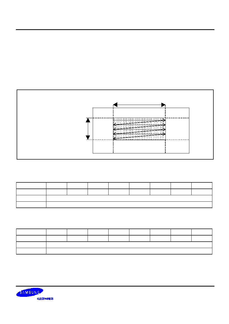
Area Scroll Function
The S6B33B0A realizes the specific area scroll function. (1/176 duty case).
0
15
161
175
Fixed area
Scroll area
Display area
LCD Panel
Fixed 15 lines
146 Lines
14
Fixed 15 lines
0
160
161
175
14
Example of Scrolling down
Example of Scrolling up
15
Figure 14. Area scroll examples (duty = 1/176, center scroll mode)

S6B33B0A PRELIMINARY VER 1.1 144 RGB SEGMENT & 177 COMMON DRIVER FOR 65,536 COLOR STN LCD
23
Display Direction
SDIR
The SDIR flag of Driver Output Mode Set instruction selects the direction of segment display.
x = 0
Y = 1
Y = 143
Y = 0
SEGA0
SEGB0
SEGC0
SEGA1
SEGB1
SEGC1
SEGA143
SEGB143
SEGC1 43
(D7~D0)
(D7~D0)
(D7~D0)
(D7~D0)
(D7~D0)
(D7~D0)
1st
2nd
Figure 15. 8-bit data bus mode when SDIR = L
Y = 1
Y = 143
Y = 0
SEGA0
SEGB0
SEGC0
SEGA1
SEGB1
SEGC1
SEGA143
SEGB143
SEGC143
(D15~D0)
(D15~D0)
(D15~D0)
X=0
Figure 16. 16-bit data bus mode when SDIR = L
x = 0
Y = 142
Y = 0
Y = 143
SEGA0
SEGB0
SEGC0
SEGA1
SEGB1
SEGC1
SEGA143
SEGB143
1
SEGC143
(D7~D0)
(D7~D0)
(D7~D0)
(D7~D0)
(D7~D0)
(D7~D0)
1st
2nd
Figure 17. 8-bit data bus mode when SDIR = H
Y = 142
Y = 0
Y = 143
SEGA0
SEGB0
SEGC0
SEGA1
SEGB1
SEGC1
SEGA143
SEGB143
SEGC1 43
(D15~D0)
(D15~D0)
(D15~D0)
x = 0
Figure 18. 16-bit data bus mode when SDIR = H

144 RGB SEGMENT & 177 COMMON DRIVER FOR 65,536 COLOR STN LCD S6B33B0A PRELIMINARY VER 1.1
24
CDIR
The direction of common scanning is selected by CDIR pin.
COM 0
COM 62
Line number 0
Line number 62
Line number 63
Display Area
128 Display Lines (DLN=00)
<CDIR=0>
Display Area
COM 87
COM 151
Line number 127
COM 1
COM 62
Line number 127
Line number 66
Line number 65
Display Area
<CDIR=1>
Display Area
COM 87
Line number 0
COM 0
COM 71
Line number 0
Line number 71
Line number 72
Display Area
144 Display Lines (DLN=01)
<CDIR=0>
Display Area
COM 87
COM 158
Line number 143
COM 0
COM 71
Line number 143
Line number 72
Line number 71
Display Area
<CDIR=1>
Display Area
COM 87
COM 158
Line number 0
COM 0
COM 80
Line number 0
Line number 80
Line number 81
Display Area
160 Display Lines (DLN=10)
<CDIR=0>
Display Area
COM 87
COM 165
Line number 159
COM 2
COM 80
Line number 159
Line number 81
Line number 80
Display Area
<CDIR=1>
Display Area
COM 87
COM 167
Line number 0
COM 0
Line number 0
Display Area
176 Display Lines (DLN=11)
<CDIR=0>
COM 175
Line number 175
COM 1
Line number 175
Display Area
<CDIR=1>
COM 176
Line number 0
COM 152
Driver
SEG144
COM176
COM 86
COM 0
COM87

S6B33B0A PRELIMINARY VER 1.1 144 RGB SEGMENT & 177 COMMON DRIVER FOR 65,536 COLOR STN LCD
25
SWP
The SWP flag of Driver Output Mode Set instruction selects the swapping of segment display.
SEGAi
SEGBi
SEGCi
RED
GREEN
BLUE
Color
SWP = 0
D15 ~ D11
D10~ D5
D4 ~ D0
Assigned Bit
BLUE
GREEN
RED
Color
SWP = 1
D4~ D0
D10 ~ D5
D15 ~ D11
Assigned Bit
Figure 19. The relationship between SEG outputs and RGB color
SWP=1
* i = 0 to 143
R control
B control
G control
D15 D14
D12 D11
D9 D8
D6 D5
D4 D3 D2
D0
RAM
DATA
SWP=0
* i = 0 to 143
B control
R control
G control
SEGAi
SEGBi
SEGCi
D4 D3
D1 D0
D9 D8 D7
D5 D15 D14 D13
D11
MPU I/F
DATA
RAM
DATA
MPU I/F
DATA
SEGAi
SEGBi
SEGCi
D2
D13
D10
D6
D12
D10
D7
D1
D15 D14
D12 D11
D9 D8
D6 D5
D4 D3 D2
D0
D13
D10
D7
D1
D15 D14
D12 D11
D9 D8
D6 D5
D4 D3 D2
D0
D13
D10
D7
D1

144 RGB SEGMENT & 177 COMMON DRIVER FOR 65,536 COLOR STN LCD S6B33B0A PRELIMINARY VER 1.1
26
On-Chip Regulator Configuration
The output voltage of regulator circuit(REG_OUT) is ranging from 1.8V to 2.2V and nominal value is 1.8V.
REG_ENB
REG_OUT
VDD
/VDDO
VDD3
/VDD3R
C1
VDD3
REG_ENB
REG_OUT
Floating
VDD3
VDD3
Value of external Capacitance
Item
Value
Unit
C1
1.0 to 4.7
�
F
VDD3: 2.4 to 3.3V
REG_OUT : 1.8V
VDD3: 1.8 to 3.3V
VDD
/VDDO
VDD3
/VDD3R
Figure 20. Regulator Application
Oscillator Circuit
When internal oscillator is used(EXT=0), the selection of oscillator resistor is determined by display mode.
-
Normal display mode/ Partial display mode 0 : resistor1 between OSC1 and OSC2
-
Partial display mode 1 : resistor2 between OSC3 and OSC4
When external clock is used (EXT=1), clock frequency should be adjusted to display mode which is selected
.
Example of external oscillator application
OSC4
OSC2
OSC3
OSC5
External clock
OSC1
VSS
Figure 21. External oscillator application

S6B33B0A PRELIMINARY VER 1.1 144 RGB SEGMENT & 177 COMMON DRIVER FOR 65,536 COLOR STN LCD
27
Example of internal oscillator application
OSC4
OSC2
OSC3
R1
OSC5
VSS/VDD3
OSC1
OSC4
OSC2
OSC3
OSC5
OSC1
VSS/VDD3
R2
R1
When partial display mode 1 is not used. When partial display mode 1 is used.
Figure 22. Internal oscillator application
Discharge Circuit
Driving voltage level discharge time at standby ON.
The relation between voltage level and discharge time from when "Standby ON" command is inputted.
LEVEL
CONDITION
T[ms]
V+,
V-[mV]
100
< 50
+VR,V1,VM,-VR
+VR=12.0V, V1=3.0V, VM=1.5V, -VR=-9.0V
at T=0
300
< 20
VM
VSS
-VR
V1
+VR
Internal STB signal
T[ms]
V+[mV]
V-[mV]

144 RGB SEGMENT & 177 COMMON DRIVER FOR 65,536 COLOR STN LCD S6B33B0A PRELIMINARY VER 1.1
28
INSTRUCTION DESCRIPTION
Table 15. Instruction Table
Instruction Name
D/I WRB RDB DB15
~ DB8 DB7
DB6
DB5 DB4
DB3
DB2 DB1 DB0 Hex. Parameter
Non Operation
0
0
1
*
0
0
0
0
0
0
0
0
00
Oscillation Mode Set
0
0
1
*
0
0
0
0
0
0
1
0
02
1Byte
Driver Output Mode Set
0
0
1
*
0
0
0
1
0
0
0
0
10
1Byte
DC-DC Select
0
0
1
*
0
0
1
0
0
0
0
0
20
1Byte
Bias Set
0
0
1
*
0
0
1
0
0
0
1
0
22
1Byte
DCDC Clock Division Set
0
0
1
*
0
0
1
0
0
1
0
0
24
1Byte
DCDC and AMP ON/OFF set
0
0
1
*
0
0
1
0
0
1
1
0
26
1Byte
Temperature Compensation Set
0
0
1
*
0
0
1
0
1
0
0
0
28
1Byte
Contrast Control(1)
0
0
1
*
0
0
1
0
1
0
1
0
2A
1Byte
Contrast Control(2)
0
0
1
*
0
0
1
0
1
0
1
1
2B
1Byte
Standby Mode OFF
0
0
1
*
0
0
1
0
1
1
0
0
2C
-
Standby Mode ON
0
0
1
*
0
0
1
0
1
1
0
1
2D
-
DDRAM Burst Mode OFF
0
0
1
*
0
0
1
0
1
1
1
0
2E
-
DDRAM Burst Mode ON
0
0
1
*
0
0
1
0
1
1
1
1
2F
-
Addressing Mode Set
0
0
1
*
0
0
1
1
0
0
0
0
30
1Byte
ROW Vector Mode Set
0
0
1
*
0
0
1
1
0
0
1
0
32
1Byte
N-line Inversion Set
0
0
1
*
0
0
1
1
0
1
0
0
34
1Byte
Entry Mode Set
0
0
1
*
0
1
0
0
0
0
0
0
40
1Byte
X-address Area Set
0
0
1
*
0
1
0
0
0
0
1
0
42
2Byte
Y-address Area Set
0
0
1
*
0
1
0
0
0
0
1
1
43
2Byte
RAM Skip Area Set
0
0
1
*
0
1
0
0
0
1
0
1
45
1Byte
Display OFF
0
0
1
*
0
1
0
1
0
0
0
0
50
-
Display ON
0
0
1
*
0
1
0
1
0
0
0
1
51
-
Specified Display Pattern Set
0
0
1
*
0
1
0
1
0
0
1
1
53
1Byte
Partial Display Mode Set
0
0
1
*
0
1
0
1
0
1
0
1
55
1Byte
Partial Display Start Line Set
0
0
1
*
0
1
0
1
0
1
1
0
56
1Byte
Partial Display End Line Set
0
0
1
*
0
1
0
1
0
1
1
1
57
1Byte
Area Scroll Mode Set
0
0
1
*
0
1
0
1
1
0
0
1
59
4Byte
Scroll Start Line Set
0
0
1
*
0
1
0
1
1
0
1
0
5A
1Byte
Set Display Data Length
X
X
X
*
1
1
1
1
1
1
0
0
FC
1Byte
Display Data Write
1
0
1
Display Data Write
-
-
Display Data Read
1
1
0
Display Data Read
-
-
Status Read
0
1
0
0
Status Data Read
-
-
Test Mode1
0
0
1
*
1
1
1
1
1
1
1
1
FF
-
Test Mode2
0
0
1
*
1
1
1
1
1
1
1
0
FE
-
Test Mode3
0
0
1
*
1
1
1
1
1
1
0
1
FD
-
Test Mode4
0
0
1
*
1
1
1
1
1
0
1
1
FB
-
Test Mode5
0
0
1
*
1
1
1
1
1
0
1
0
FA
-
Test Mode6
0
0
1
*
1
1
1
1
1
0
0
1
F9
-
*: Don't care
Parameter: The number of parameter bytes that follows instruction data.

S6B33B0A PRELIMINARY VER 1.1 144 RGB SEGMENT & 177 COMMON DRIVER FOR 65,536 COLOR STN LCD
29
Non Operation (00H)
This instruction is Non operation.
D/I
WRB
RDB
DB7
DB6
DB5
DB4
DB3
DB2
DB1
DB0
0
0
1
0
0
0
0
0
0
0
0
Oscillation Mode Set (02H)
Setting internal function mode.
D/I
WRB
RDB
DB7
DB6
DB5
DB4
DB3
DB2
DB1
DB0
0
0
0
0
0
0
1
0
0
0
1
0
0
0
0
0
0
EXT
OSC
EXT: External clock selecting
EXT = 0: Internal clock mode (Initial status)
EXT = 1: External clock mode
OSC: Internal oscillator ON/OFF
OSC = 0: Internal oscillator OFF(Initial status)
OSC = 1: Internal oscillator ON
Driver Output Mode Set(10H)
This instruction sets the display direction.
D/I
WRB
RDB
DB7
DB6
DB5
DB4
DB3
DB2
DB1
DB0
0
0
0
1
0
0
0
0
0
0
1
0
0
DLN
0
SDIR
SWP
0
DLN: Display Line number selecting
DB5
DB4
Display Duty
0
0
1/128
0
1
1/144
1
0
1/160
1
1
1/176
SDIR: Segment direction
This bit is for controlling the direction of segment driver.
SDIR = 0 (Initial status)
SWP: Swap segment output SEGAi and SEGCi
This bit is for swapping the output of segment driver.
SWP = 0 (Initial status)

144 RGB SEGMENT & 177 COMMON DRIVER FOR 65,536 COLOR STN LCD S6B33B0A PRELIMINARY VER 1.1
30
DC-DC Select (20H)
Selects DC-DC step-up of the common driver in normal and partial mode
D/I
WRB
RDB
DB7
DB6
DB5
DB4
DB3
DB2
DB1
DB0
0
0
1
0
0
0
0
0
0
0
1
0
0
0
0
DC(2)
DC(1)
DC(1) : 1'st DC-DC booster boosting step select for V1 generation in normal mode and partial mode 0.
DC(2) : 1'st DC-DC booster boosting step select for V1 generation in partial mode 1.
DC(2) : In partial mode 1
DC(1) : In normal mode, partial mode 0
DB3
DB2
DC-DC step up
DB1
DB0
DC-DC step up
0
0
X1.0
0
0
X1.0
0
1
X1.5
0
1
X1.5
1
0
X2.0
1
0
X2.0
1
1
X2.0
1
1
X2.0

S6B33B0A PRELIMINARY VER 1.1 144 RGB SEGMENT & 177 COMMON DRIVER FOR 65,536 COLOR STN LCD
31
DC-DC Select and power supply for V1 Op-Amp.
Even if VIN45 is connected to VOUT45 or VIN1, a setup by software must be able to be performed.
Power supply for V1 Op.Amp. is decided by Hardware setting and Software setting.
The example of usage is shown below.
Hardware setting : VIN45 connected to (1) VIN1 (when 1'st boosting is not used)
(2) VOUT45 (when 1'st boosting is used)
Software setting : DC-DC Select(20H) - DC(1), DC(2)
Set value "00" Power supply for V1 Op.Amp. uses VIN1 directly.
Set value "01" or "10" Power supply for V1 Op.Amp. uses VOUT45.
1st
Booster
Circuit
Reference
voltage
generator
&
Temperature
Compensation
Control Circuit
VIN1
V1
+
C11-
C11+
C12-
C12+
VOUT45
VIN45
-
R1
EV_256
R1
Software Setting
Hardware Setting
V1 generation circuit
Figure28. Example : Hardware Setting
Software Setting
: VIN45 connected to VOUT45
: Power supply for V1 Op.Amp. uses VIN1 ( not VOUT45).
VSS

144 RGB SEGMENT & 177 COMMON DRIVER FOR 65,536 COLOR STN LCD S6B33B0A PRELIMINARY VER 1.1
32
Bias Set (22H)
This instruction set up the value of bias in normal mode and in partial mode.
D/I
WRB
RDB
DB7
DB6
DB5
DB4
DB3
DB2
DB1
DB0
0
0
1
0
0
0
1
0
0
0
1
0
0
Bias(2)
0
0
Bias(1)
Bias(1): Bias value selecting in normal mode and partial mode0.
Bias(2): Bias value selecting in partial mode1.
Bias (2) : In partial mode 1
Bias (1) : In normal mode, partial mode 0
DB5
DB4
Bias(2) 2'nd boosting step DB1
DB0
Bias(1)
2'nd boosting step
0
0
1/4
x(-3)
0
0
1/4
x(-3)
0
1
1/5
x(-4)
0
1
1/5
x(-4)
1
0
1/6
x(-4)
1
0
1/6
x(-4)
1
1
1/7
x(-5)
1
1
1/7
x(-5)
DCDC Clock Division Set(24H)
This instruction sets the internal booster clock frequency.
D/I
WRB
RDB
DB7
DB6
DB5
DB4
DB3
DB2
DB1
DB0
0
0
1
0
0
1
0
0
0
0
1
0
0
DIV(2)
0
0
DIV(1)
DIV(1) : DC-DC Charge Pump Division Ratio in Normal Mode Display and Partial Display Mode0
- DIV(1) = 10 (Initial status)
DIV(2) : Division Ratio in Partial Display Mode1
- DIV(2) = 10 (Initial status)
DB5
DB4
DIV(2)
DB1
DB0
DIV(1)
0
0
fPCK = fOSC/4
0
0
fPCK = fOSC/4
0
1
fPCK = fOSC/8
0
1
fPCK = fOSC/8
1
0
fPCK = fOSC/16
1
0
fPCK = fOSC/16
1
1
fPCK = fOSC/32
1
1
fPCK = fOSC/32
Note: fOSC = ( ROUNDUP (Duty/3) + dummy) x 4 x 8 x frame frequency

S6B33B0A PRELIMINARY VER 1.1 144 RGB SEGMENT & 177 COMMON DRIVER FOR 65,536 COLOR STN LCD
33
DC/DC and AMP ON/OFF Set (26H)
This instruction set up the DC/DC and Op-amp in common start up setting.
D/I
WRB
RDB
DB7
DB6
DB5
DB4
DB3
DB2
DB1
DB0
0
0
1
0
0
1
1
0
0
0
1
0
0
0
0
AMP
DCDC3 DCDC2 DCDC1
AMP: Built-in OP-AMP ON/OFF.
- AMP=0: OP-AMP OFF (Initial status)
- AMP=1: OP-AMP ON
DCDC1: Built-in 1'st Booster ON/OFF
- DCDC1= 0: 1'st Booster OFF (Initial status)
- DCDC1= 1: 1'st Booster ON
DCDC2: Built-in 2'nd Booster ON/OFF
- DCDC2= 0: 2'nd Booster OFF (Initial status)
- DCDC2= 1: 2'nd Booster ON
DCDC3: Built-in 3'rd Booster ON/OFF
- DCDC3= 0: 3'rd Booster OFF (Initial status)
- DCDC3= 1: 3'rd Booster ON
Temperature Compensation Set (28H)
This Instruction sets up the driving voltage slope for temperature compensation.
D/I
WRB
RDB
DB7
DB6
DB5
DB4
DB3
DB2
DB1
DB0
0
0
1
0
1
0
0
0
0
0
1
0
0
0
0
0
0
TCS
TCS: Temperature compensation slope set
-
TCS = 00 : 0.00%/degC (Initial status)
-
TCS = 01 : -0.05%/degC
-
TCS = 10 : -0.10%/degC
-
TCS = 11 : -0.15%degC
00: 0.00 %/degC
Driving
voltage
01: -0.05 %/degC
10: -0.10 %/degC
11: -0.15 %/degC
Temperature
25degC

144 RGB SEGMENT & 177 COMMON DRIVER FOR 65,536 COLOR STN LCD S6B33B0A PRELIMINARY VER 1.1
34
Temperature Compensation
If external temperature compensation is needed, circuit diagram is described as below.
To use temperature compensation, two resistors and one thermistor are needed.
External
Chip
Internal
V1IN
+
-
V1OUT
V1T
INTRS

S6B33B0A PRELIMINARY VER 1.1 144 RGB SEGMENT & 177 COMMON DRIVER FOR 65,536 COLOR STN LCD
35
Contrast Control (1) (2AH)
This instruction updates the contrast control value in normal display mode and partial display mode 0.
D/I
WRB
RDB
DB7
DB6
DB5
DB4
DB3
DB2
DB1
DB0
0
0
1
0
1
0
1
0
0
0
1
Contrast control value (0 to 255)
The relation between V1 voltage (typ.) and Contrast(1) set value ( 3bit step case)
Contrast(1)
(HEX)
V1
[V]
Contrast(1)
(HEX)
V1
[V]
Contrast(1)
(HEX)
V1
[V]
Contrast(1)
(HEX)
V1
[V]
Contrast(1)
(HEX)
V1
[V]
Contrast(1)
(HEX)
V1
[V]
00h
2.000
30h
2.376
60h
2.753
90h
3.129
C0h
3.506
F0h
3.882
08h
2.063
38h
2.439
68h
2.816
98h
3.192
C8h
3.569
F8h
3.945
10h
2.125
40h
2.502
70h
2.878
A0h
3.255
D0h
3.631
FFh
4.000
18h
2.188
48h
2.565
78h
2.941
A8h
3.318
D8h
3.694
20h
2.251
50h
2.627
80h
3.004
B0h
3.380
E0h
3.757
28h
2.314
58h
2.690
88h
3.067
B8h
3.443
E8h
3.820
Contrast Control (2) (2BH)
This instruction updates the contrast control value in partial display mode 1.
D/I
WRB
RDB
DB7
DB6
DB5
DB4
DB3
DB2
DB1
DB0
0
0
1
0
1
0
1
1
0
0
1
Contrast control value (0 to 255)
The relation between V1 voltage (typ.) and Contrast(2) set value ( 3 bit step case)
Contrast(2)
(HEX)
V1
[V]
Contrast(2)
(HEX)
V1
[V]
Contrast(2)
(HEX)
V1
[V]
Contrast(2)
(HEX)
V1
[V]
Contrast(2)
(HEX)
V1
[V]
Contrast(2)
(HEX)
V1
[V]
00h
2.000
30h
2.376
60h
2.753
90h
3.129
C0h
3.506
F0h
3.882
08h
2.063
38h
2.439
68h
2.816
98h
3.192
C8h
3.569
F8h
3.945
10h
2.125
40h
2.502
70h
2.878
A0h
3.255
D0h
3.631
FFh
4.000
18h
2.188
48h
2.565
78h
2.941
A8h
3.318
D8h
3.694
20h
2.251
50h
2.627
80h
3.004
B0h
3.380
E0h
3.757
28h
2.314
58h
2.690
88h
3.067
B8h
3.443
E8h
3.820
Note :
S6B33B0A has a hardware protection for "2VR < 20V". It means the limitation of contrast value in each bias.
If 1/6 bias is set, max contrast value is limited to A9h, and if 1/7 bias is set, max contrast value is limited to 6Dh.

144 RGB SEGMENT & 177 COMMON DRIVER FOR 65,536 COLOR STN LCD S6B33B0A PRELIMINARY VER 1.1
36
Standby Mode OFF (2CH)
This instruction releases the standby mode.
D/I
WRB
RDB
DB7
DB6
DB5
DB4
DB3
DB2
DB1
DB0
0
0
1
0
0
1
0
1
1
0
0
The internal statuses during standby off are as following:
-
All common and segment output: VSS or V1
-
Oscillator circuit: On (EXT = 0, OSC=1),OFF (others)
-
Displaying clocks (FR, PM, CL): In operation
Function and Pin condition at standby OFF
Function/Pin
Condition
DC/DC
booster(1'st,2'nd,3'rd)
ON(Operate)
COM outputs
+VR or VM or VSS or -VR
SEG outputs
V1 or VSS
Standby Mode ON (2DH)
This instruction enters the standby mode to reduce the power consumption to the static power consumption
value (Initial status). The following instructions, standby off and display on, cause returning to the normal
operation status.
D/I
WRB
RDB
DB7
DB6
DB5
DB4
DB3
DB2
DB1
DB0
0
0
1
0
0
1
0
1
1
0
1
The internal statuses during standby on are as following:
-
All common and segment output: VSS
-
Oscillator circuit: OFF
-
Displaying clocks (FR, PM, CL) are held.
Function and Pin condition at standby ON
Function/Pin
Condition
DC/DC
booster(1'st,2'nd,3'rd)
OFF
SEG and COM outputs
VSS
LCD driving power output condition at Standby ON.
level
Condition
+VR
VSS
V1
VSS
VM
VSS
-VR
VSS

S6B33B0A PRELIMINARY VER 1.1 144 RGB SEGMENT & 177 COMMON DRIVER FOR 65,536 COLOR STN LCD
37
DDRAM Burst Mode OFF(2EH) /ON(2FH)
D/I
WRB
RDB
DB7
DB6
DB5
DB4
DB3
DB2
DB1
DB0
0
0
1
0
0
1
0
1
1
1
BM
BM: Internal DDRAM Burst Mode Interface Off/On Control
- 0 : Burst Mode Interface Off(Initial Status)
- 1 : Burst Mode Interface On
When BM=0, If MPU[0] is 0 then internal DDRAM I/F bpw(bits per word) is 8 bits.
Else MPU[0] is 1 then internal DDRAM I/F bpw(bits per word) is 16bits.
When BM=1, Regardless of MPU[0] bit, Internal DDRAM I/F bpw(bits per word) is 32 bits
.
MPU
Register1
00H 01H
DDRAM
X Address
Counter
32
16
8
8
Register2
02H 03H
8EH 8FH
- - - - - - - - -
Y Address
Counter
8
S6B33B0
Figure 23. Burst mode writing to DDRAM

144 RGB SEGMENT & 177 COMMON DRIVER FOR 65,536 COLOR STN LCD S6B33B0A PRELIMINARY VER 1.1
38
/CS
E
DB15
~DB0
Burst
Mode
ON
X
Address
Setting
Y
Address
Setting
RAM
DATA
1(16bits)
- - - - - - - - -
- - - - - - - - -
RAM
DATA
2(16bits)
RAM
DATA
3(16bits)
RAM
DATA
4(16bits)
- - - - -
- - - - -
- - - - -
RAM Write time
RAM Write time
RAM write data (32 bits)
RAM data 1 to 2
RAM data 3 to 4
RAM
DATA
5(16bits)
RAM
DATA
6(16bits)
RAM Write time
RAM data 5 to 6
RAM X address
RAM Y address
00H
00H
02H
04H
- - - - -
- - - - -
- - - - -
Figure 24. Example of the Burst mode writing to DDRAM (68-mode 16-bit parallel interface)
When DDRAM burst mode is used, note the following.
Notes:
1.Data is written to DDRAM each two words. If only one word data is written to DDRAM, the data will not
be written.
So, the number of word data must be even. It means that Y start address must be even and Y end
address must be odd.
2.X address count mode can't be used.
3.Burst mode and normal mode write operation cannot be executed at the same time.
4.In the read data mode and serial interface mode, the burst mode can't be used.
5.In the 256 color mode with 16-bit data bus mode and 4,096 color mode with 8-bit data bus mode,
The address is counted as burst mode enable. So these modes are influenced by
above notes.

S6B33B0A PRELIMINARY VER 1.1 144 RGB SEGMENT & 177 COMMON DRIVER FOR 65,536 COLOR STN LCD
39
Addressing Mode Set (30H)
D/I
WRB
RDB
DB7
DB6
DB5
DB4
DB3
DB2
DB1
DB0
0
0
1
1
0
0
0
0
0
0
1
0
GSM
DSG
SGF
SGP
SGM
GSM: Gray Scale Mode
- 00 : 65,536 color mode(Initial status)
- 01 : 4,096 color mode* (refer to "Data Format Select(60H/61H)")
- 10 : 256 color mode*
- 11 : 256 color mode*
* In the 256 color mode with 16-bit data bus mode and 4,096 color mode with 8-bit data format B,
the address is counted as burst mode enable. So, In this case, refer to notes of burst mode at page 39.
DSG : Duty Adjust Setting
- 0 : Dummy subgroup is one subgroup (Initial status)
- 1 : Dummy subgroup is none
SGF : Sub Group Frame Inversion mode setting
- 0: SG Frame inversion OFF (Initial status)
- 1: SG Frame inversion ON
SGM : Sub Group inversion mode setting
- 0: SG inversion OFF (Initial status)
- 1: SG inversion ON
SGP : Sub Group Phase mode setting
- 00 : Same phase in all pixels
- 01 : Different phase by 1pixel-unit
- 10 : Different phase by 2pixel-unit
- 11 : Different phase by 4pixel-unit
Row Vector Mode Set (32H)
Setting ROW function.
D/I
WRB
RDB
DB7
DB6
DB5
DB4
DB3
DB2
DB1
DB0
0
0
1
1
0
0
1
0
0
0
1
0
0
0
0
INC
VEC
INC: Row Vector Increment Mode. This Parameter set up Row vector increment period
DB3
DB2
DB1
Row Vector Increment Period
0
0
0
Every subgroup
0
0
1
Every 2subgroup
0
1
0
Every 4subgroup
0
1
1
Every 8subgroup
1
0
0
Every 16subgroup
1
0
1
Every 16subgroup
1
1
0
Every 16subgroup
1
1
1
Every subframe
VEC: ROW Vector Sequence Mode
- 0: R1->R2->R3->R4 -> R1..... (initial status)
- 1: R1->R3->R2->R4 -> R1.....

144 RGB SEGMENT & 177 COMMON DRIVER FOR 65,536 COLOR STN LCD S6B33B0A PRELIMINARY VER 1.1
40
256 Color Mode Palettes
At 256-color mode, the instruction and parameter below set each Gray Scale level of the Red/Green/Blue.
Gray scale level is determined by GS data.
Red Palette (38H)
D/I
WRB
RDB
DB7
DB6
DB5
DB4
DB3
DB2
DB1
DB0
0
0
1
1
1
0
0
0
0
0
0
GS data "000" to RAM data
0
0
0
GS data "001" to RAM data
0
0
0
GS data "010" to RAM data
0
0
0
GS data "011" to RAM data
0
0
0
GS data "100" to RAM data
0
0
0
GS data "101" to RAM data
0
0
0
GS data "110" to RAM data
0
0
1
0
0
0
GS data "111" to RAM data
Green Palette (3AH)
D/I
WRB
RDB
DB7
DB6
DB5
DB4
DB3
DB2
DB1
DB0
0
0
1
1
1
0
1
0
0
0
GS data "000" to RAM data
0
0
GS data "001" to RAM data
0
0
GS data "010" to RAM data
0
0
GS data "011" to RAM data
0
0
GS data "100" to RAM data
0
0
GS data "101" to RAM data
0
0
GS data "110" to RAM data
0
0
1
0
0
GS data "111" to RAM data
Blue Palette (3CH)
D/I
WRB
RDB
DB7
DB6
DB5
DB4
DB3
DB2
DB1
DB0
0
0
1
1
1
1
0
0
0
0
0
GS data "00" to RAM data
0
0
0
GS data "01" to RAM data
0
0
0
GS data "10" to RAM data
0
0
1
0
0
0
GS data "11" to RAM data

S6B33B0A PRELIMINARY VER 1.1 144 RGB SEGMENT & 177 COMMON DRIVER FOR 65,536 COLOR STN LCD
41
Initial value for each Palette
Initial Gray Scale Level
Gray Scale
Data
Red
Green
Blue
000
0
0
0
001
8
16
12
010
12
24
20
011
16
32
31
100
20
40
-
101
24
48
-
110
28
56
-
111
31
63
-
The relationship between Gray Scale level and RAM data for Red/Blue
RAM Data
RAM Data
DB4
DB3
DB2
DB1
DB0
GS Level
DB4
DB3
DB2
DB1
DB0
GS Level
0
0
0
0
0
0
1
0
0
0
0
16
0
0
0
0
1
1
1
0
0
0
1
17
0
0
0
1
0
2
1
0
0
1
0
18
0
0
0
1
1
3
1
0
0
1
1
19
0
0
1
0
0
4
1
0
1
0
0
20
0
0
1
0
1
5
1
0
1
0
1
21
0
0
1
1
0
6
1
0
1
1
0
22
0
0
1
1
1
7
1
0
1
1
1
23
0
1
0
0
0
8
1
1
0
0
0
24
0
1
0
0
1
9
1
1
0
0
1
25
0
1
0
1
0
10
1
1
0
1
0
26
0
1
0
1
1
11
1
1
0
1
1
27
0
1
1
0
0
12
1
1
1
0
0
28
0
1
1
0
1
13
1
1
1
0
1
29
0
1
1
1
0
14
1
1
1
1
0
30
0
1
1
1
1
15
1
1
1
1
1
31

144 RGB SEGMENT & 177 COMMON DRIVER FOR 65,536 COLOR STN LCD S6B33B0A PRELIMINARY VER 1.1
42
The relationship between Gray Scale level and Gray Scale data for Green
GS Data
GS Data
DB5 DB4 DB3 DB2 DB1 DB0
GS Level
DB5 DB4 DB3 DB2 DB1 DB0
GS Level
0
0
0
0
0
0
0
1
0
0
0
0
0
32
0
0
0
0
0
1
1
1
0
0
0
0
1
33
0
0
0
0
1
0
2
1
0
0
0
1
0
34
0
0
0
0
1
1
3
1
0
0
0
1
1
35
0
0
0
1
0
0
4
1
0
0
1
0
0
36
0
0
0
1
0
1
5
1
0
0
1
0
1
37
0
0
0
1
1
0
6
1
0
0
1
1
0
38
0
0
0
1
1
1
7
1
0
0
1
1
1
39
0
0
1
0
0
0
8
1
0
1
0
0
0
40
0
0
1
0
0
1
9
1
0
1
0
0
1
41
0
0
1
0
1
0
10
1
0
1
0
1
0
42
0
0
1
0
1
1
11
1
0
1
0
1
1
43
0
0
1
1
0
0
12
1
0
1
1
0
0
44
0
0
1
1
0
1
13
1
0
1
1
0
1
45
0
0
1
1
1
0
14
1
0
1
1
1
0
46
0
0
1
1
1
1
15
1
0
1
1
1
1
47
0
1
0
0
0
0
16
1
1
0
0
0
0
48
0
1
0
0
0
1
17
1
1
0
0
0
1
49
0
1
0
0
1
0
18
1
1
0
0
1
0
50
0
1
0
0
1
1
19
1
1
0
0
1
1
51
0
1
0
1
0
0
20
1
1
0
1
0
0
52
0
1
0
1
0
1
21
1
1
0
1
0
1
53
0
1
0
1
1
0
22
1
1
0
1
1
0
54
0
1
0
1
1
1
23
1
1
0
1
1
1
55
0
1
1
0
0
0
24
1
1
1
0
0
0
56
0
1
1
0
0
1
25
1
1
1
0
0
1
57
0
1
1
0
1
0
26
1
1
1
0
1
0
58
0
1
1
0
1
1
27
1
1
1
0
1
1
59
0
1
1
1
0
0
28
1
1
1
1
0
0
60
0
1
1
1
0
1
29
1
1
1
1
0
1
61
0
1
1
1
1
0
30
1
1
1
1
1
0
62
0
1
1
1
1
1
31
1
1
1
1
1
1
63

S6B33B0A PRELIMINARY VER 1.1 144 RGB SEGMENT & 177 COMMON DRIVER FOR 65,536 COLOR STN LCD
43
N-block inversion Set (34H)
This instruction set up N block inversion for AC driving.
D/I
WRB
RDB
DB7
DB6
DB5
DB4
DB3
DB2
DB1
DB0
0
0
1
1
0
1
0
0
0
0
1
FIM
FIP
0
N-block inversion
FIM: Forcing Inversion Mode
FIM = 0: Forcing Inversion OFF (Initial status)
FIM = 1: Forcing Inversion ON
FIP: Forcing Inversion Period
FIP = 0: Forcing Inversion Period is one frame
FIP = 1: Forcing Inversion Period is two frames
N-block Inversion : This parameter indicates the basic period of polarity inversion.
The whole period of polarity inversion is decided by FIM, FIP and this parameter.
DB7
DB6
DB5
DB4 � DB0
Polarity Inversion Period
x
X
x
0
every frame
0
X
x
1
every 1 block
:
:
:
:
:
0
X
x
31
every 31 blocks
1
0
x
1
every 1 block and every frame
:
:
:
:
:
1
0
x
31
every 31 blocks and every frame
1
1
x
1
every 1 block and every 2 frames
:
:
:
:
:
1
1
x
31
every 31 blocks and every 2 frames

144 RGB SEGMENT & 177 COMMON DRIVER FOR 65,536 COLOR STN LCD S6B33B0A PRELIMINARY VER 1.1
44
Entry Mode Set (40H)
Setting internal function mode.
D/I
WRB
RDB
DB7
DB6
DB5
DB4
DB3
DB2
DB1
DB0
0
1
0
0
0
0
0
0
0
0
1
0
0
0
0
HL
MDI
X/Y
RMW
HL: When GSM is 10 or 11 (256 color mode),
Exchange higher and lower byte in 16-bit data bus mode only for "Display Data Write/Read"
HL = 0: Not exchanged status (Initial status)
HL = 1: Exchanged status
MDI: Memory data inversion setting for low power consumption.
MDI = 0: Memory data inversion OFF (Initial status)
MDI = 1: Memory data inversion ON
X/Y: Memory address counter mode setting
X/Y = 0: Y address counter mode (Initial status)
X/Y = 1: X address counter mode
RMW: Read modify write mode ON/OFF select
RMW = 0: Read modify write OFF (Initial status)
RMW = 1: Read modify write ON. When this mode is on, X(Y) address of on-chip display RAM is not
increment in reading display data but in writing display data.
X Address Area Set (42H)
This instruction and parameter set up the X address areas of the on-chip display data RAM.
D/I
WRB
RDB
DB7
DB6
DB5
DB4
DB3
DB2
DB1
DB0
0
1
0
0
0
0
1
0
X start address set (Initial Status = 00H)
0
0
1
X end address set (Initial Status = AFH)
The current X address of the on-chip display data RAM is the X start address by setting this instruction. In X
address count mode (X/Y = "H"), the X address is increased from X start address to X end address. When X
address is equal to the X end address, the Y address is increased by 1 and the X address returns to X start
address. The X start and X end addresses must be set as a pair and X start address must be less than X end
address.
<MDI=0>
Data Bus
Memory
Display Data Write Display Data Read
<MDI=1>
Display Data Write Display Data Read
00h
00h
00h
FFh
00h
00h
FFh
00h

S6B33B0A PRELIMINARY VER 1.1 144 RGB SEGMENT & 177 COMMON DRIVER FOR 65,536 COLOR STN LCD
45
Y Address Area Set (43H)
This instruction and parameter set up the Y address areas of the on-chip display data RAM
.
D/I
WRB
RDB
DB7
DB6
DB5
DB4
DB3
DB2
DB1
DB0
0
1
0
0
0
0
1
1
Y start address set (Initial Status = 00H)
0
0
1
Y end address set (Initial Status = 8FH)
The current Y address of the on-chip display data RAM is the Y start address by setting this instruction. In
Y address count mode (X/Y = "L"), the Y address is increased from Y start address to Y end address. When
Y address is equal to the Y end address, the X address is increased by 1 and the Y address returns to Y start
address. The Y start and Y end address must be set as a pair and Y start address must be less than Y end
address.
RAM Skip Area Set (45H)
This instruction and parameter set up the X address areas of the on-chip display data RAM.
D/I
WRB
RDB
DB7
DB6
DB5
DB4
DB3
DB2
DB1
DB0
0
1
0
0
0
1
0
1
0
0
1
0
0
0
0
0
0
RSK
RSK : RAM Skip function ON/OFF set
-
RSK = 00 : No Skip
-
RSK = 01 : Y address 44h-4Bh skip
-
RSK = 10 : Y address 40h-4Fh skip
-
RSK = 11 : Y address 3Ch-53h skip
RAM Skip Area Set
RAM Skip Area Set can skip a part of RAM Y-address area. After setting RAM skip area, Y-address count
skip this area and count. In other words, Y address after skip area is changed into Y address which added a
part for skip area.
Memory data
Input Display Area
Skip Area
X-address
Area
Y-address Area

144 RGB SEGMENT & 177 COMMON DRIVER FOR 65,536 COLOR STN LCD S6B33B0A PRELIMINARY VER 1.1
46
Display OFF (50H)
Turn the display OFF(Initial status).
When display is off, all segment and common output are VSS level.
D/I
WRB
RDB
DB7
DB6
DB5
DB4
DB3
DB2
DB1
DB0
0
0
1
0
1
0
1
0
0
0
0
Function and Pin condition at Display OFF
Function/Pin
Condition
DC/DC
booster(1'st,2'nd,3'rd)
ON(Operate)
SEG and COM outputs
VSS
Display ON (51H)
Turns the display ON.
In case of being standby mode, this instruction does not work. This instruction is executed after standby mode
off.
D/I
WRB
RDB
DB7
DB6
DB5
DB4
DB3
DB2
DB1
DB0
0
0
1
0
1
0
1
0
0
0
1
Function and Pin condition at Display ON
Function/Pin
Condition
DC/DC
booster(1'st,2'nd,3'rd)
ON(Operate)
COM outputs
+VR or VM or -VR
SEG outputs
V1 or VSS
Specified Display Pattern Set (53H)
This instruction sets the specified display pattern.
D/I
WRB
RDB
DB7
DB6
DB5
DB4
DB3
DB2
DB1
DB0
0
1
0
1
0
0
1
1
0
0
1
0
0
0
0
0
0
SDP
SDP : Specified Display Pattern set
- SDP = 00 : Normal display
- SDP = 01 : Reverse display : Display data reversing mode setting without the contents of the display
RAM
-
SDP = 10 : Whole display pattern becomes OFF regardless of the RAM data.
-
SDP = 11 : Whole display pattern becomes ON regardless of the RAM data.
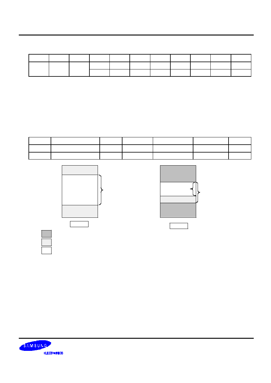
S6B33B0A PRELIMINARY VER 1.1 144 RGB SEGMENT & 177 COMMON DRIVER FOR 65,536 COLOR STN LCD
47
Partial Display Mode Set (55H)
D/I
WRB
RDB
DB7
DB6
DB5
DB4
DB3
DB2
DB1
DB0
0
1
0
1
0
1
0
1
0
0
1
0
0
0
0
0
0
PDM
PT
PT: Partial Display ON/OFF
-
PT = 0: Partial display OFF = Normal mode (Initial status)
-
PT = 1: Partial display ON
PDM: Partial Display mode set
-
PDM = 0: Partial mode 0 : Duty ratio is same as Normal display mode(initial status)
-
PDM = 1: Partial mode 1 : Duty ratio is changed from Normal display mode
(DSG = 0 : 69 line fixed(including 1 dummy subgroup),
DSG = 1 : 66 line fixed(no dummy subgroup))
Applied parameter in PDM0 and PDM1 are summarized as below
PDM
Contrast
Duty
Bias
DC-DC Select
OSC
PCK
0
Contrast control(1)
Normal
Bias(1)
DC(1)
OSC1-OSC2
DIV(1)
1
Contrast control(2)
1/69
Bias(2)
DC(2)
OSC3-OSC4
DIV(2)
Operation in Partial Display Mode 0 (PDM=0)
On
scanning except partial display area
- SEG output select V0 or V1 level depend on "FR" value. Refer to Page51.
- All of COM output is fixed VM level.
On scanning partial display area
- It is equal to be in normal mode
Operation in Partial Display Mode 1 (PDM=1)
Display area is from partial start line to partial end line.
(COM driver output is fixed VM except display area, only max69 line output COM signal.
On
scanning except partial display area
- SEG output select V0 or V1 level depend on "FR" value. Refer to Page51.
- All of COM output is fixed VM level.
On scanning partial display area
- It is equal to be in normal mode
Display
Area
Partial Start Line
Partial End Line
N line
PDM 0
Partial Start Line
M line
69 line Fix
PDM 1
No display Area : No COM Scanning field (COM = Vm fixed)
Except Partial Display Area : COM Timing is existing, but COM = Vm fixed
Partial Display Area : Real display field
Partial End Line

144 RGB SEGMENT & 177 COMMON DRIVER FOR 65,536 COLOR STN LCD S6B33B0A PRELIMINARY VER 1.1
48
Partial Display Mode0
Item
Partial Display Area
Out of Partial Display Area
Duty
Same as normal display mode
Bias
Same as normal display mode ( Bias(1) setting )
Contrast
Same as normal display mode ( Contrast(1) setting )
Oscillator
Same as normal display mode ( OSC1 � OSC2 )
SEG Output level
Same as normal mode (V1,V0)
Depends on Internal "FR" signal
See page 51
COM Output level
Same as normal mode
(+VR,VM,-VR)
VM fixed
Partial display mode1
Item
Partial Display Area
Out of Partial Display Area
Out of Display Area
Duty
1/69duty
Bias
Bias(2) setting
Contrast
Contrast(2) setting
Oscillator
( OSC3 � OSC4 ) setting value
SEG Output
level
Same as normal mode
(V1,V0)
Depends on "FR" signal
See page 51
-
COM Output
level
Same as normal mode
(+VR, VM, -VR)
VM fixed
VM fixed
<COM0-2>
In case of COM 6 to COM11 Partial display
<COM3-5>
<COM6-8>
<COM9-11>
<COM12-14>
Normal Display Mode
Partial Display Mode 1
+VR
VM
-VR

S6B33B0A PRELIMINARY VER 1.1 144 RGB SEGMENT & 177 COMMON DRIVER FOR 65,536 COLOR STN LCD
49
Partial Display Start Line Set (56H), Partial Display End Line Set(57H)
These 2 instructions set the partial display area and it is possible to display a part.
Partial Display Start Line Set (56H)
D/I
WRB
RDB
DB7
DB6
DB5
DB4
DB3
DB2
DB1
DB0
0
1
0
1
0
1
1
0
0
0
1
Partial start line
Partial Display End Line Set (57H)
D/I
WRB
RDB
DB7
DB6
DB5
DB4
DB3
DB2
DB1
DB0
0
1
0
1
0
1
1
1
0
0
1
Partial end line
Parameter set appoints display line number. At PDM 0, Parameter Size is able to be in a number of Display
lines. But that is not able to be over max 69 line at PDM 1. Partial end line must set bigger number than Partial
start line.
line 0
line 1
COM 0
COM 1
line 2
line 3
COM 2
COM 3
line 172
line 173
COM 172
line 174
line 175
COM 173
COM 174
COM 175
:
:
:

144 RGB SEGMENT & 177 COMMON DRIVER FOR 65,536 COLOR STN LCD S6B33B0A PRELIMINARY VER 1.1
50
Example of Segment Voltage in non-display area
Area scroll Set (59H)
This instruction sets up area scroll field (start line, end line, Lower fixed line number), and it is possible to make
screen to display as partial scroll field.
D/I
WRB
RDB
DB7
DB6
DB5
DB4
DB3
DB2
DB1
DB0
0
1
0
1
1
0
0
1
0
0
0
0
0
0
SCM
Scroll area start line
Scroll area end line
0
0
1
Lower fixed number
SCM: Scroll mode setting
DB1
DB0
Mode
0
0
Entire display(Initial status)
0
1
Upper scroll display
1
0
Lower scroll display
1
1
Center scroll display
COM
Partial
Display
VM
Subframe
+VR
VM
-VR
V1
VM
V0
Addressing Duty
Display
Off
internal
polarity
counter
(FR)
V0
V1
V0
V1
V0
V1
V1
V0
V1
V0
VM
VM
VM
0
1
2
0
3
N
N+1
SEG
Frame

S6B33B0A PRELIMINARY VER 1.1 144 RGB SEGMENT & 177 COMMON DRIVER FOR 65,536 COLOR STN LCD
51
Entire Display
Upper Display
Lower Display
Center Display
Scroll Start Line Set (5AH)
This instruction and parameter set up scroll start line. On this instruction, scroll start line becomes the first of
area scroll field. Scroll operation is occurred every issue of this instruction.
D/I
WRB
RDB
DB7
DB6
DB5
DB4
DB3
DB2
DB1
DB0
0
1
0
1
1
0
1
0
0
0
1
Scroll start line
<Example>
-DLN : 2'b11 (1/176 duty)
-SCM : 2'b11 (Center display mode)
-Scroll area start line : 6
-Scroll area end line : 166
-Lower fixed number : 9
-Scroll start line : 40
Upper
fIx
<DUTY BLOCK>
<RAM BLOCK>
COM6
COM175
COM0
Scroll
area
Upper
fix
Scroll
display
Lower
fix
<DISPLAY>
Xadr=6
Xadr=0
Xadr=167
Xadr=175
RAM Address.
COM167
COM0
COM6
COM175
COM167
Lower
fix
Addr0
Addr5
Addr40
Addr167
Addr175
Addr166
Addr6
Addr39
Xadr=40

144 RGB SEGMENT & 177 COMMON DRIVER FOR 65,536 COLOR STN LCD S6B33B0A PRELIMINARY VER 1.1
52
Data Format Select (60H/61H)
D/I
WRB
RDB
DB7
DB6
DB5
DB4
DB3
DB2
DB1
DB0
0
0
1
0
1
1
0
0
0
0
DFS
DFS: 4,096 Color Mode Data Format Select
- 0 : 4,096 Color Data Format A (Initial Status)
8 bit mode :
DB[7:0] : XXXXRRRR (1'st write)
DB[7:0] : GGGGBBBB(2'nd write)
16 bit mode :
DB[15:0] :XXXXRRRRGGGGBBBB (12 bit)
- 1 : 4,096 Color Data Format B
8 bit mode :
DB[7:0] : RRRRGGGG(1'st write)
DB[7:0] : BBBBRRRR (2'nd write)
DB[7:0] : GGGGBBBB(3'rd write)
16 bit mode :
DB[15:0] :RRRRGGGGBBBBXXXX (12 bit)
Normal Mode
Normal Mode
Partial Mode 0
Scroll Mode
Scroll/Partial Mode 0
Set partial start line
Set partial end line
Set partial mode 0
Set scroll mode
Set scroll area start line
Set scroll area end line
Set lower fixed line no.
Set scroll start line
Set scroll mode
Set scroll area start line
Set scroll area end line
Set lower fixed line
Set scroll start line
Set partial start line
Check busy flag
Set partial end line
Set partial mode 0
Release partial mode
Set scroll mode
Set scroll area start line
Set scroll area end line
Set lower fixed line no.
Set scroll start line
Set scroll mode
Set scroll area start line
Set scroll area end line
Set lower fixed line no.
Set scroll start line
Release partial mode

S6B33B0A PRELIMINARY VER 1.1 144 RGB SEGMENT & 177 COMMON DRIVER FOR 65,536 COLOR STN LCD
53
Display Data Write/Read
D/I
WRB
RDB
DB15
~ DB8
DB7
DB6
DB5
DB4
DB3
DB2
DB1
DB0
1
0
1
Display RAM write in data
1
1
0
Display RAM read out data
GSM = 00(65,536 Color Mode)
(1) 16bit access mode
15 14 13
12 11 10
9
8
7
6
5
4
3
2
1
0
1'st cycle
R4 R3 R2 R1 R0 G5 G4 G3 G2 G1 G0 B4 B3 B2 B1 B0
2'nd cycle
R4 R3 R2 R1 R0 G5 G4 G3 G2 G1 G0 B4 B3 B2 B1 B0
(2) 8bit access mode
7
6
5
4
3
2
1
0
1'st cycle
R4 R3 R2 R1 R0 G5 G4 G3
2'nd cycle
G2 G1 G0 B4 B3 B2 B1 B0
3'rd cycle
R4 R3 R2 R1 R0 G5 G4 G3
4'th cycle
G2 G1 G0 B4 B3 B2 B1 B0
GSM = 01(4,096 Color Mode)
(1) 16bit access mode
15 14 13
12 11 10
9
8
7
6
5
4
3
2
1
0
1'st cycle
X
X
X
X
R3 R2 R1 R0 G3 G2 G1 G0 B3 B2 B1 B0
2'nd cycle
X
X
X
X
R3 R2 R1 R0 G3 G2 G1 G0 B3 B2 B1 B0
(2) 8bit access mode
7
6
5
4
3
2
1
0
1'st cycle
X
X
X
X
R3 R2 R1 R0
2'nd cycle
G3 G2 G1 G0 B3 B2 B1 B0
3'rd cycle
X
X
X
X
R3 R2 R1 R0
4'th cycle
G3 G2 G1 G0 B3 B2 B1 B0
GSM = 10 or 11 (256 Color Mode)
(1) 16bit access mode
15 14 13
12 11 10
9
8
7
6
5
4
3
2
1
0
1'st cycle
R2 R1 R0 G2 G1 G0 B1 B0 R2 R1 R0 G2 G1 G0 B1 B0
2'nd cycle
R2 R1 R0 G2 G1 G0 B1 B0 R2 R1 R0 G2 G1 G0 B1 B0
(2) 8bit access mode
7
6
5
4
3
2
1
0
1'st cycle
R2 R1 R0 G2 G1 G0 B1 B0
2'nd cycle
R2 R1 R0 G2 G1 G0 B1 B0
3'rd cycle
R2 R1 R0 G2 G1 G0 B1 B0
4'th cycle
R2 R1 R0 G2 G1 G0 B1 B0

144 RGB SEGMENT & 177 COMMON DRIVER FOR 65,536 COLOR STN LCD S6B33B0A PRELIMINARY VER 1.1
54
Status Read
D/I
WRB
RDB
DB7
DB6
DB5
DB4
DB3
DB2
DB1
DB0
0
1
0
BSY
X/Y
0
PDM
PT
STB
REV
DP
This instruction indicates the internal status of the S6B33B0A.
DP: ( 0 : Display OFF Status, 1 : Display ON Status )
REV: ( 0 : Display Image Non-Reversing, 1 : Display Image Reversing )
STB: ( 0 : Standby Mode OFF Status, 1 : Standby Mode ON Status )
PT: ( 0 : Partial Display Mode OFF Status, 1 : Partial Display Mode ON Status )
PDM: ( 0 : Partial Display Mode 0, 1 : Partial Display Mode 1 )
X/Y: ( 0 : Y-address Count Mode, 1 : X-address Count Mode )
BSY: ( 0 : No Busy, 1 : Busy )
Set Display Data Length (FCH)
This Instruction is only used in 3-pin SPI MPU interface mode(PS="L", MPU[1]="L"). It consists of two
continuous commands, the first byte control the data direction(write mode only) and inform the LCD driver the
second and third bytes will be number of data bytes will be write. When DI is not used, the Display Data Length
instruction is used to indicate that a specified number of display data bytes are to be transmitted.
The next byte after the display data string is handled as command data.
D/I
WRB
RDB
DB7
DB6
DB5
DB4
DB3
DB2
DB1
DB0
1
1
1
1
1
1
0
0
Number of display data upper 8bits (DDL_H)
0
0
1
Number of display data lower 8bits (DDL_L)

S6B33B0A PRELIMINARY VER 1.1 144 RGB SEGMENT & 177 COMMON DRIVER FOR 65,536 COLOR STN LCD
55
Test Mode1 (FFH)
This Instruction is for testing IC. User is not permitted to access. if access, have to reset.
D/I
WRB
RDB
DB7
DB6
DB5
DB4
DB3
DB2
DB1
DB0
0
0
1
1
1
1
1
1
1
1
1
Test Mode2 (FEH)
This Instruction is for testing IC. User is not permitted to access. if access, have to reset.
D/I
WRB
RDB
DB7
DB6
DB5
DB4
DB3
DB2
DB1
DB0
0
0
1
1
1
1
1
1
1
1
0
Test Mode3 (FDH)
This Instruction is for testing IC. User is not permitted to access. if access, have to reset.
D/I
WRB
RDB
DB7
DB6
DB5
DB4
DB3
DB2
DB1
DB0
0
0
1
1
1
1
1
1
1
0
1
Test Mode4 (FBH)
This Instruction is for testing IC. User is not permitted to access. if access, have to reset.
D/I
WRB
RDB
DB7
DB6
DB5
DB4
DB3
DB2
DB1
DB0
0
0
1
1
1
1
1
1
0
1
1
Test Mode5 (FAH)
This Instruction is for testing IC. User is not permitted to access. if access, have to reset.
D/I
WRB
RDB
DB7
DB6
DB5
DB4
DB3
DB2
DB1
DB0
0
0
1
1
1
1
1
1
0
1
0
Test Mode6 (F9H)
This Instruction is for testing IC. User is not permitted to access. if access, have to reset.
D/I
WRB
RDB
DB7
DB6
DB5
DB4
DB3
DB2
DB1
DB0
0
0
1
1
1
1
1
1
0
0
1

144 RGB SEGMENT & 177 COMMON DRIVER FOR 65,536 COLOR STN LCD S6B33B0A PRELIMINARY VER 1.1
56
INSTRUCTION PARAMETER
Table 16. Instruction Parameter
Instruction
Hex Para.
DB7
DB6
DB5
DB4
DB3
DB2
DB1
DB0
0
0
0
0
0
0
EXT
OSC
Oscillation Mode Set
02H
1
*
*
*
*
*
*
0
0
0
0
DLN
0
SDIR
SWP
0
Driver Output Mode Set
10H
1
*
*
0
0
*
0
0
0
0
0
0
0
DC(2)
DC(1)
DC-DC Set
20H
1
0
0
0
0
0
0
0
0
0
0
Bias(2)
0
0
Bias(1)
Bias Set
22H
1
0
*
0
0
*
*
0
0
0
0
DIV(2)
0
0
DIV(1)
DCDC Clock Division Set
24H
1
*
*
1
0
*
*
1
0
0
0
0
0
AMP
DCDC3 DCDC2 DCDC1
DCDC and AMP ON/OFF Set
26H
1
*
*
*
*
0
0
0
0
0
0
0
0
0
0
TCS
Temperature Compensation Set 28H
1
*
*
*
*
*
*
0
0
Contrast control value in normal and partial display mode0(0 to 255)
Contrast Control (1)
2AH
1
0
0
0
0
0
0
0
0
Contrast control value in partial display mode 1(0 to 255)
Contrast Control(2)
2BH
1
0
0
0
0
0
0
0
0
0
GSM
DSG
SGF
SGP
SGM
Addressing Mode Set
30H
1
*
*
0
0
0
0
0
0
0
0
0
0
INC
VEC
ROW Vector Mode Set
32H
1
*
*
*
*
0
0
0
0
FIM
FIP
0
N-block Inversion
N-line Inversion Set
34H
1
0
0
*
0
0
0
0
0
0
0
0
0
HL
MDI
X/Y
RMW
Entry Mode Set
40H
1
*
*
*
*
*
0
0
0
X Start address set
0
0
0
0
0
0
0
0
X end address set
X-address Area Set
42H
2
1
0
1
0
1
1
1
1
Y start address set
0
0
0
0
0
0
0
0
Y end address set
Y-address Area Set
43H
2
1
0
0
0
1
1
1
1
0
0
0
0
0
0
RSK
RAM Skip Area Set
42H
1
*
*
*
*
*
*
0
0
Number of display data DDL_H
Set Display Data Length
FCH
2
Number of display data DDL_L
0
0
0
0
0
0
SDP
Specified Display Pattern Set
53H
1
*
*
*
*
*
*
0
0
0
0
0
0
0
0
PDM
PT
Partial Display Mode Set
55H
1
*
*
*
*
*
*
0
0
Partial start line
Partial Display Start Line Set
56H
1
0
0
0
0
0
0
0
0
Partial end line
Partial Display End Line Set
57H
1
0
0
0
0
0
0
0
0

S6B33B0A PRELIMINARY VER 1.1 144 RGB SEGMENT & 177 COMMON DRIVER FOR 65,536 COLOR STN LCD
57
Table 16. Instruction Parameter (Continued)
Instruction
Hex
Para.
DB7
DB6
DB5
DB4
DB3
DB2
DB1
DB0
0
0
0
0
0
0
SCM
*
*
*
*
*
*
0
0
Scroll area start line
0
0
0
0
0
0
0
0
Scroll area end line
1
0
1
0
1
1
1
1
Lower Fixed number
Area Scroll Mode Set
59H
4
0
0
0
0
0
0
0
0
Scroll start line
Scroll Start Line Set
5AH
1
0
0
0
0
0
0
0
0

144 RGB SEGMENT & 177 COMMON DRIVER FOR 65,536 COLOR STN LCD S6B33B0A PRELIMINARY VER 1.1
58
Reset Operation
When RSTB becomes "L", following procedure is occurred.
- X start address: 0, X end address: 176
- Y start address: 0, Y end address: 143
- Display OFF
- Read Modify Write Mode OFF
- Function Mode Set
MDI = 0: Memory Data Inversion OFF
OSC = 0: Oscillator OFF
EXT = 0: Internal Oscillator Mode
REV = 0: Reversing mode OFF
X/Y = 0: Y-address Count Mode
Standby Mode ON
- DCDC Clock Division Set
DIV(1) = 10: fPCK = fOSC/16x
DIV(2) = 10: fPCK = fOSC/16x
- Duty Set
Display Duty = 00H: 1/128 duty
- DC-DC Select
DC(1) = 0: X1 step-up
DC(2) = 0: X1 step-up
- Bias Set
Bias(1) = 0H: 1/4 bias
Bias(2) = 0H: 1/4 bias
- DC/DC and AMP ON/OFF Set
AMP =0: Built-in OP-AMP OFF
DCDC1 =0: Built-in 1'st booster OFF
DCDC2 =0: Built-in 2'nd booster OFF
DCDC3 =0: Built-in 3'rd booster OFF
- N-block inversion
FIM =0: Forcing Inversion OFF
FIP =0: Forcing Inversion Period in one frame
N-block inversion = 00H: frame inversion
- Partial Display Mode
PT = 0: Partial Display Mode OFF
PDM = 0: Partial Mode 0
- Partial Display Area Set
Partial start line = 00H
Partial end line = 00H
-Area Scroll Set
Mode = 00H : Entire Display Scroll Mode
Area Start Line: 00H
Area End Line: AFH
Lower Fixed Line Number: 00H
- Scroll Start Line Set
Scroll Start Line: 00H
- Addressing Mode Set
GSM=00: 65,536 Color Mode
DSG = 0: Mode 0
SGF = 0: SG Frame Inversion OFF
SGM = 0: SG Reverse Mode OFF
SGP=00:Same phase in all pixel
- Row Vector Mode Set
INC =000: Increment every subgroup
VEC=0: R1->R2->R3->R4->R1->...

S6B33B0A PRELIMINARY VER 1.1 144 RGB SEGMENT & 177 COMMON DRIVER FOR 65,536 COLOR STN LCD
59
POWER ON/OFF SEQENCE
Power ON Sequence
Power On
Reset
Waiting for
releasingReset
Standby
mode OFF
Busy Flag
check or
waiting for
OSC ON
DCDC1 ON
AMP ON
DCDC2 ON
No busy
Busy
Set various registers and RAM data if needed
(XS,XE,YS,YE,MDI,EXT,REV,XY,DIV,DLN,BIAS,DC,
FIM,FIP,N-block,PT,PDM,SMOD,DSG,GSM,SGF,
SGM,SGP,INC,VEC, Display Data)
Display ON
DCDC3 ON

144 RGB SEGMENT & 177 COMMON DRIVER FOR 65,536 COLOR STN LCD S6B33B0A PRELIMINARY VER 1.1
60
Power OFF Sequence
Standby On
( DCDC3 OFF
DCDC2 OFF
AMP OFF
DCDC1 OFF
OSC OFF )
Waiting for
Discharge
Power Off
Display Off

S6B33B0A PRELIMINARY VER 1.1 144 RGB SEGMENT & 177 COMMON DRIVER FOR 65,536 COLOR STN LCD
61
SPECIFICATIONS
ABSOLUTE MAXIMUM RATINGS
Item
Symbol
Rating
Unit
Supply Voltage range
VDD3
-0.3 to +4.0
V
LCD Supply Voltage range
|
VCC � VEE|
22
V
Input Voltage range
Vin
- 0.3 to VDD +0.3
V
Operating Temperature range
T
OPR
-30 to +70
�
C
Storage Temperature range
T
STR
-55 to +150
�
C
OPERATING VOLTAGE
Item
Symbol
Min.
Typ.
Max.
Unit
Supply Voltage (1)
VDD3
1.8
-
3.3
V
Supply Voltage (2)
2Vr
4.0
-
20
V
Supply Voltage (3)
VIN
2.4
3.0
3.6
V

144 RGB SEGMENT & 177 COMMON DRIVER FOR 65,536 COLOR STN LCD S6B33B0A PRELIMINARY VER 1.1
62
DC CHARACTERISTICS (1)
(Vss
= 0V, V
DD3
= 1.8 to 3.3V, Ta = -30 to 70
�
C)
Item
Symbol
Condition
Min
Typ
Max
Uni
t
Remarks
Operating voltage
VDD3
1.8
3.3
V
VDD3
Operating voltage
VIN1
2.4
-
3.6
V
VIN1,VIN1A
Operating voltage
VIN2
2.4
-
7.2
V
Operating voltage
VIN45
2.4
-
7.2
V
VOUT45
1/4 Bias
1.5
-
3.0
1/5 Bias
1.33
-
2.67
1/6 Bias
1.67
-
3.33
Operating voltage
DC2IN
1/7 Bias
1.5
-
3.0
V
DC2OUT
Operating voltage
2Vr
2Vr
= |(+VR)- (-VR)|
4.0
-
20
V
+VR, -VR
VM
1.0
2.0
V
VMOUT
VCC
5.0
12.0
V
VRP
Driving voltage input
range
VEE
External power supply
mode
-3.0
-8.0
V
VRN
High
V
IH
0.8VDD
-
VDD
Input
voltage
Low
V
IL
VSS
-
0.2VDD
V
High
V
OH
I
OH
= 0.5mA
0.8VDD
-
VDD
Output
voltage
Low
V
OL
I
OL
= 0.5mA
VSS
-
0.2VDD
V
Input leakage current
I
IL
VIN = VDD or VSS
-1.0
-
+1.0
�
A
Output leakage current
I
OZ
VIN = VDD or VSS
-3.0
-
+3.0
�
A
Normal or
Partial 0
F
OSC1
R1=80kOhm
(fFR=100Hz target),
DSG=0, 176 display lines
172.8
192.0
211.2
kHz OSC1 -
OSC2
Oscillator
Frequency
Tolerance
Partial 1
F
OSC2
R1=300kOhm
(fFR=70Hz target),
69 display lines
46.36
51.52
56.68
kHz OSC3 -
OSC4
Normal or
Partial 0
F
OSC1
(*1)
84.48
288
kHz OSC1 -
OSC2
Oscillator
Frequency
Range
Partial 1
F
OSC2
(*2)
29.44
88.32
kHz OSC3 -
OSC4
Driving voltage input
range
V1
VM
2.0
1.0
-
4.0
2.0
V
Regulator output range
REG_OUT
REG_ENB = "L"
1.8
-
2.2
V
(*1) Minimum oscillator frequency range is defined at fFR=60Hz and display line number=128
Maximum oscillator frequency range is defined at fFR=150Hz and display line number=176
(*2) Minimum oscillator frequency range is defined at fFR=40Hz and display line number=69

S6B33B0A PRELIMINARY VER 1.1 144 RGB SEGMENT & 177 COMMON DRIVER FOR 65,536 COLOR STN LCD
63
Maximum oscillator frequency range is defined at fFR=120Hz and display line number=69
DC CHARACTERISTICS (2)
Item
Symbol
Condition
Min
Typ
Max
Unit Remarks
SEG
R
ON-Seg
V1=3.0 V, V0=0V,
Ta = 25
�
C, Iload=50uA
-
1.5
3.0
k
SEGn
Driver output
resistance
COM
R
ON-Com
VCC=10.5 V, VM=1.5V,
VEE=-7.5V,
Ta = 25
�
C, Iload=100uA
-
1.0
1.5
k
COMn
Normal
Mode
VDD3=VIN1=3.0V, V1=3.0V,
Bias(1)=1/6, DC(1)=x1.5,
Ta=25
�
C, Display line=176
DSG=0 (1dummy)
f
OSC
1=192.0kHz (fFR=100Hz)
Low current mode, No load,
No access, All white pattern
-
650
750
�
Current
consumption
Partial1
Mode
IDD
VDD3=VIN1=3.0V, V1=3.0V,
Bias(2)=1/5, DC(2)=x1.5,
Ta=25
�
C, 1/69 duty
f
OSC
2=51.52kHz (fFR=70Hz)
Low current mode, No load,
No access, All white pattern
-
200
250
�
VDD3
+ VIN1
* : "IDD" is determined from lowest power consumption for dc-dc converter.

144 RGB SEGMENT & 177 COMMON DRIVER FOR 65,536 COLOR STN LCD S6B33B0A PRELIMINARY VER 1.1
64
DC CHARACTERISTICS (3)
(Vss
= 0V, V
DD3
= 1.8 to 3.3V, VIN1=2.4 to 3.6V, Ta = -30 to 70
�
C)
Item
Symbol
Condition
Min
Typ
Max Unit Remarks
(+VR)
Isource = 80uA
-
-
150
mV
+VR
(V1)
Isource = 250uA
-
-
20
mV
V1
(VM)
Isource,sink = 250uA
-
-
20
mV
VM
Voltage shift range(*1)
(-VR)
Isink = 80uA
-
-
150
mV
-VR
(*1) Voltage shift means output voltage deference between output current = Iload and no-load.
Refer to the following figure. (in case of source current mode)
Item
Symbol
Condition
Min
Typ
Max
Unit Remarks
Tolerance of Bias ratio
(+VR)_0
(-VR)_0(*1)
No load
-100
-
+100
mV +VR
-VR
(*1) Tolerance of bias ratio definition
(+VR)_0 = ((+VR) - VM ) � VM / Bias
(-VR)_0 = ( VM - (-VR)) � VM / Bias
No-load
Vx
Vx
Vy
Vy
I=0
I=ILoad
Vshift = |Vx-Vy|
Current = I Load

S6B33B0A PRELIMINARY VER 1.1 144 RGB SEGMENT & 177 COMMON DRIVER FOR 65,536 COLOR STN LCD
65
DC CHARACTERISTICS (4)
(Vss
= 0V, V
DD3
= 1.8 to 3.3V, VIN1=2.4 to 3.6V, Ta = -30 to 70
�
C)
Item
Symbol
Condition
Min
Typ
Max
Unit
Remarks
Temperature
compensation
Vt
VDD3=VIN1=V1=3.0V,
-20 to 70
�
C
-0.02
-
+0.02
%/
�
C
V1
Tolerance of Contrast
step of V1
Vstep
3.13
6.27
9.41
mV
V1
V1
3.95
4.00
4.05
V
V1
Contrast set = FFh
VM
1.95
2.00
2.05
V
VM
V1
1.95
2.00
2.05
V
V1
Voltage range
V1
VM
Contrast set = 00h
VM
0.95
1.00
1.05
V
VM
Condition
Item
Load current
Voltage range
Max
Unit
Ref
||+VR-VM| -|VM -(-VR)||
I Load = +100uA (+VR)
I Load = -100uA (-VR)
100
mV
Fig.1
A
I Load = +100uA ( V1, VM )
Offset
Voltage
||V1-VM| -|VM-V0||
B
I Load = +100uA (+VR)
I Load = -100uA (-VR)
+VR=5.0~12.0 V
V1=2.0~4.0V
VM=1.0~2.0V
-VR=-3.0~-8.0 V
50
mV
Fig.2
+VR
Fig. 1: Offset voltage definition (+VR,VM,-VR)
Vx
|Vx-Vy| < 100mV
VM
-VR
Vy
+100uA
-100uA
V1
Va
|Va-Vb| < 50mV
VM
V0
Vb
+100uA (both Case A and B)
-100uA (Case B)
+100uA (Case A)
Fig. 2: Offset voltage definition (V1,VM,V0)

144 RGB SEGMENT & 177 COMMON DRIVER FOR 65,536 COLOR STN LCD S6B33B0A PRELIMINARY VER 1.1
66
DC CHARACTERISTICS (5)
(Vss
= 0V, V
DD3
= 1.8 to 3.3V, VIN1=2.4 to 3.6V, Ta = -30 to 70
�
C)
Range
Item
Min
Max
V1OUT
2.0 V
4.0 V (DC(1) and DC(2) = X2) (*1)
VMOUT
1.0 V
2.0 V (DC(1) and DC(2) = X2) (*2)
Voltage Level
DC2OUT
1.33V
(1/5 Bias, V1OUT = 2V)
3.33V (DC(1) and DC(2) = X2) (*3)
(1/6 Bias, V1OUT = 4V)
If V1OUT input voltage is set over VIN45,
V1OUT output voltage must be clipped near VIN45.
In this case, V1OUT output level must not be
unstable. Refer to Fig.1
V1OUT
VIN45
Delta V > 0.3 V (External VIN45)
Delta V
(*1) This definition is shown as below
VIN45
V1OUT
Output
VIN45
VIN45 - Delta V
Fig. 1
V1OUT
Input
Delta V > 0.5 V (VIN45 = VOUT45)
If VMOUT input voltage is set over VIN1,
VMOUT output voltage must be clipped near
VIN1.
In this case, VMOUT output level must not be
unstable. Refer to Fig.2
VMOUT
VIN1
Delta V > 0.3 V
Delta V
(*2) This definition is shown as below
VIN1
VMOUT
Output
VIN1
VIN1 - Delta V
Fig. 2
VMOUT
Input
If DC2OUT input voltage is set over VIN2,
DC2OUT output voltage must be clipped near VIN2.
In this case, VMOUT output level must not be
unstable. Refer to Fig.3
DC2OUT
VIN2
Delta V > 0.3 V (External VIN2)
Delta V
(*3) This definition is shown as below
VIN2
DC2OUT
Output
VIN2
VIN2 - Delta V
Fig. 3
DC2OUT
Input
Delta V > 0.5 V (VIN2 = VOUT45)

S6B33B0A PRELIMINARY VER 1.1 144 RGB SEGMENT & 177 COMMON DRIVER FOR 65,536 COLOR STN LCD
67
AC CHARACTERISTICS
Read / Write Characteristics (8080-series MPU)
DB0 to DB7
(Write)
DB0 to DB7
(Read)
t
DH80
t
OD80
t
DS80
t
ACC80
0.9V
DD
0.1V
DD
t
PW L80(R)
, t
PWL80(W)
t
CY80
t
AH80
t
AS80
/RD, /WR
/CS1
(CS2)
D/I
t
PWH80(R)
, t
PW H80(W)
** t
PWL80(W)
and t
PWL80(R)
is specified in the overlapped period when CS1B is low (CS2 is high)
and /WR(/RD) is low.
Figure 25. Parallel Interface (8080-series MPU) Timing Diagram
Table 17. AC Characteristics (8080-series Parallel Mode)
(VDD3
= 1.8 to 3.3V, Ta = -30 to +70
�
C)
Min.
Item
Signal
Symbol
Condition
3.3V
1.8V
Max.
(3.3V/1.8V) Unit
Address setup time
Address hold time
D/I
t
AS80
t
AH80
0
0
0
0
-
-
ns
System cycle time
t
CY80
150
360
-
ns
Pulse width low for write
Pulse width High for write
WRB
(WRB)
t
PWLW
t
PWHW
50
30
100
75
-
-
ns
Pulse width low for read
Pulse width high for read
RDB
(RDB)
t
PWLR
t
PWHR
50
30
100
75
-
-
ns
Data setup time
Data hold time
t
DS80
t
DH80
5
8
10
14
-
-
ns
-
60 / 120
Read access time
Output disable time
DB0
to
DB15
t
ACC80
t
OD80
CL = 100 pF
tEWHR
ns
NOTE: *1. The input signal rise time and fall time (tr, tf) is specified at 10 ns or less.
(tr + tf) < (t
CY80
- t
PWLW
- t
PWHW
) for write, (tr + tf) < (t
CY80
- t
PWLR
- t
PWHR
) for read

144 RGB SEGMENT & 177 COMMON DRIVER FOR 65,536 COLOR STN LCD S6B33B0A PRELIMINARY VER 1.1
68
Read / Write Characteristics (6800-series Microprocessor)
t
DH68
t
OD68
t
DS68
t
ACC68
0.9V
DD
0.1V
DD
t
EW H68(R)
, t
EWH68(W)
t
CY68
t
AH68
t
AS68
DB0 to DB7
(Write)
E
/CS1
(CS2)
D/I,R/W
DB0 to DB7
(Read)
t
EWL68(R)
, t
EWL68(W)
** t
EWH68(W)
and t
EWH68(R)
is specified in the overlapped period when /CS1 is low (CS2 is high)
and E is high.
Figure 26. Parallel Interface (6800-series MPU) Timing Diagram
Table 18. AC Characteristics (6800-series Parallel Mode)
(V
DD3
= 1.8 to 3.3V, Ta = -30 to +70
�
C)
Min.
Item
Signal
Symbol
Condition
3.3V
1.8V
Max.
(3.3V/1.8V) Unit
Address setup time
Address hold time
D/I
R/W
t
AS68
t
AH68
0
0
0
0
-
-
ns
System cycle time
t
CY68
150
360
-
ns
Enable width high for write
Enable width low for write
RDB
(E)
t
EWHW
t
EWLW
50
30
100
75
-
-
ns
Enable width high for read
Enable width low for read
RDB
(E)
t
EWHR
t
EWLR
50
30
100
75
-
-
ns
Data setup time
Data hold time
t
DS68
t
DH68
5
8
10
14
-
-
ns
-
60 / 120
Read access time
Output disable time
DB0
to
DB15
T
ACC68
t
OD68
C
L
= 100 pF
tEWLR
ns
NOTE: *1. The input signal rise time and fall time (tr, tf) is specified at 10 ns or less.
(tr + tf) < (t
CY68
- t
EWHW
- t
EWLW
) for write, (tr + tf) < (t
CY68
- t
EWHR
- t
EWLR
) for read

S6B33B0A PRELIMINARY VER 1.1 144 RGB SEGMENT & 177 COMMON DRIVER FOR 65,536 COLOR STN LCD
69
Serial Data Interface Timing
/CS1
SDI
D/I
SCL
t
CSH
t
SDH
t
SAH
t
SCYC
t
CSS
t
SDS
t
SAS
t
SLW
t
SHW
t
f
0.1V
DD
0.1V
DD
t
r
0.9V
DD
0.1V
DD
0.9V
DD
0.1V
DD
(CS2)
Table 19. Serial Data Interface Timing
(V
DD3
= 1.8 to 3.3V, Ta = -30 to +70
�
C)
Item
Signal
Symbol
Condition
Min.
Max.
Unit
SCL Cycle Time
SCL
t
CSC
50
-
ns
SCL High Pulse Width
SCL
t
SHW
20
-
ns
SCL Low Pulse Width
SCL
t
SLW
20
-
ns
SDI Setup time
SDI
t
SDS
20
-
ns
SDI Hold time
SDI
t
SDH
20
-
ns
D/I Setup time
D/I
t
SAS
20
-
ns
D/I Hold time
D/I
t
SAH
20
-
ns
Chip Select Setup time
CS1B(CS2)
t
CSS
20
-
ns
Chip Select Hold time
CS1B(CS2)
t
CHS
20
-
ns
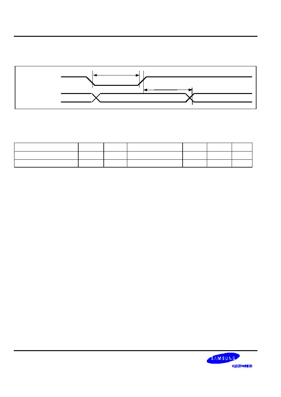
144 RGB SEGMENT & 177 COMMON DRIVER FOR 65,536 COLOR STN LCD S6B33B0A PRELIMINARY VER 1.1
70
Reset Input Timing
/RST
Internal status
t
RW
t
R
Reset complete
During reset
Figure 27. Reset Input Timing Diagram
Table 20. AC Characteristics (Reset mode)
(V
DD3
= 1.8 to 3.3V, Ta = -30 to +70
�
C)
Item
Signal
Symbol
Condition
Min.
Max.
Unit
Reset low pulse width
RSTB
t
RW
1000
-
ns
Reset time
-
t
R
-
1000
ns
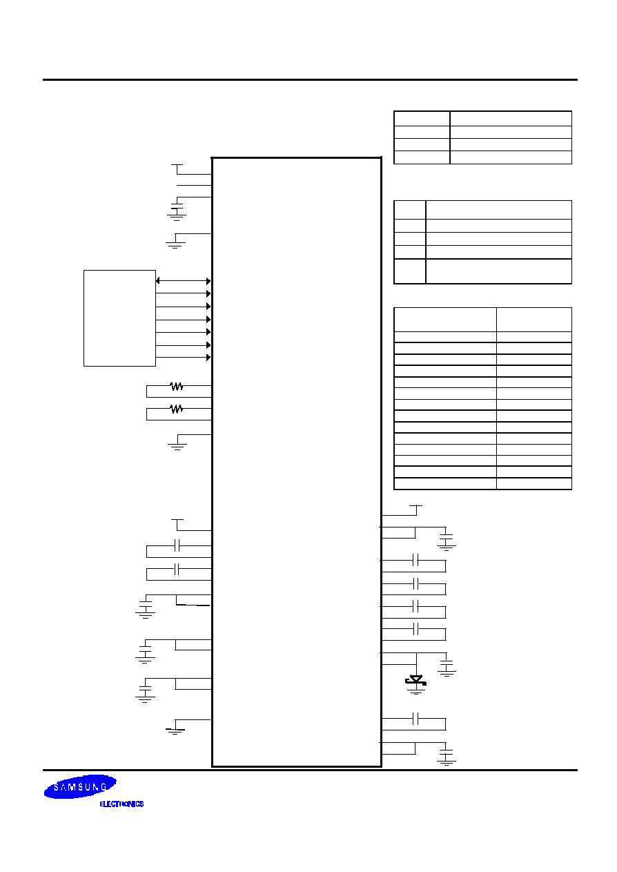
S6B33B0A PRELIMINARY VER 1.1 144 RGB SEGMENT & 177 COMMON DRIVER FOR 65,536 COLOR STN LCD
71
SYSTEM APPLICATION DIAGRAM
Internal Power Mode
External Components
Name
Device
R1,R2
Resistors
C1,C2,C3
Capacitors
D1
Schottky barrier diode
Values of external Capacitors and D1
Item
Capacitance
C1
1.0 to 4.7
�
F
C2
1.0 to 2.2
�
F
C3
1.0 to 2.2
�
F
D1 Vforward = Max. 0.3V at 1mA
Vreverse = Min. 15V
Maximum rating voltage of capacitors
Item
Maximum
rating voltage
REG_OUT to VSS
3V
VOUT45 to VSS
11V
C11P to C11M
6V
C12P to C12M
6V
VMOUT to VSS
3V
DC2OUT to VSS
5V
V1OUT to VSS
6V
C21P to C21M
5V
C22P to C22M
10V
C23P to C23M
13V
C24P to C24M
13V
VSS to VRN
13V
C31P to C31M
17V
VRP to VSS
18V
S6B33B0A
OSC1
OSC2
OSC3
OSC4
R1
R2
OSC5
/WR
/RD
DB15DB0
D/I
/CS1
/WR
/RD
DB15 to DB0
MPU
CS2
D/I
/RST
/CS1
CS2
C11P
C11M
C12P
C12M
C2
C2
VOUT45
VIN45
C3
VIN1, VIN1A
VIN1
VDD3, VDD3R
VDD, VDDO
REG_OUT
VDD3 or REG_OUT
C1
C21P
C21M
C22P
C22M
C2
C2
C23M
C24P
C24M
C2
C2
VRN
VEES, VEE
C3
VIN2
VIN2
DC2OUT
DC2IN
C3
V1OUT
V1IN
C3
VMOUT
VMIN
C3
C31P
C31M
C2
VRP
VCC
C3
C23P
V0IN
VSS, VSSA, VSSB, VSSO
/RST
D1

144 RGB SEGMENT & 177 COMMON DRIVER FOR 65,536 COLOR STN LCD S6B33B0A PRELIMINARY VER 1.1
72
External Power Mode
S6B33B0A
OSC1
OSC2
OSC3
OSC4
R1
R2
OSC5
/WR
/RD
DB15 to DB0
D/I
/
RST
/CS1
/WR
/RD
DB15 to DB0
MPU
CS2
D/I
/RST
/CS1
CS2
C11P
C11M
C12P
C12M
VDD3, VDD3R
VDD, VDDO
REG_OUT
VDD3 or REG_OUT
C
VOUT45
VIN45
VIN1, VIN1A
VIN1
C21P
C21M
C22P
C22M
C23P
C23M
C24P
C24M
VRN
VEES, VEE
VIN2
VIN2
DC2OUT
DC2IN
V1OUT
V1IN
VMOUT
VMIN
C31P
C31M
VRP
VCC
V1IN
VMIN
VEE
VCC
V0IN
VSS, VSSA, VSSB, VSSO