INFRAED REMOCON RECEIVER
S5G9801X01/S5G9803X01
1
INTRODUCTION
The S5G9801X01 and S5G9803X01 are CMOS integrated circuits for
the infrared ray remote receiver, used with the S5G9802, which can
be applied to TV, VCR, VDP, CDP and AV controller.
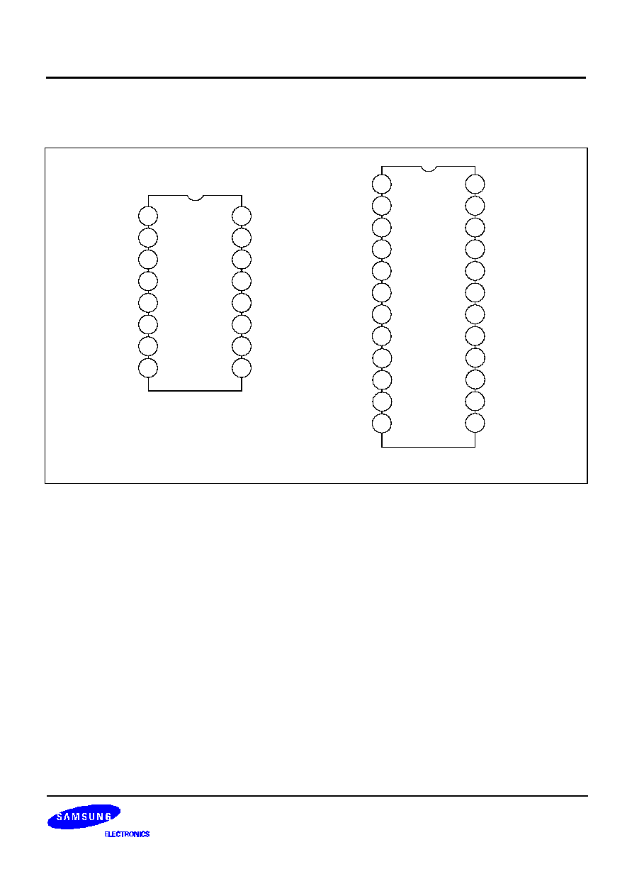
The S5G9801X01 is a 16-DIP type and is able to control 10 functions.
The S5G9803X01 is a 24-DIP type and is able to control 18 functions.
FEATURES
∑
Output for continuous pulse, toggle pulse and single pulse are
provided (Toggle pulse is available only for S5G9803X01)
∑
A single terminal type oscillator by means of RC is provided
∑
Containing custom code detection circuit for code check with
the transmitter (To prevent interferences with other models)
∑
Able to output in parallel method multiple keying signals sent
from transmitter.
The S5G9801X01 can output up to 5 functions, and the S5G9803X01 can output up to 6 functions in parallel
method.
ORDERING INFORMATION
Device
Package
Operating Temperature
S5G9801X01-D0B0
16
-
DIP
-
300A
-
20
∞
C
-
+75
∞
C
S5G9803X01-D0B0
24
-
DIP
-
400
24
-
DIP
-
400
16
-
DIP
-
300A
S5G9801X01/S5G9803X01
INFRAED REMOCON RECEIVER
4
PIN DESCRIPTION
ABSOLUTE MAXIMUM RATINGS (TA = 25◊C)
Pin No
Symbol
Input
Output
Description
S5G9801 S5G9803
1
1
GND
Ground
-
2
2
REMIN
Receiving Signal
Input
Instruction signal input with the carrier signal
eliminated.
3
-
7
-
CP1
-
SP5
Continuous Signal
output
As long as receiving is input, this output is held at
"
H
"
level. After releasing a key, output is held at
"
H
"
level
for about 160 msec.
-
3
-
8
CP1
-
CP6
-
9
-
10
TP1, TP2
Toggle Signal
Output
When receiving signal is input, output is toggled.
8 ~ 12
-
SP1
-
SP5
Single Signal Output
When receiving signal is input, output is held at
"
H
"
level only for about 107 msec.
-
11
-
20
SP1
-
SP10
13, 14
21, 22
CODE
Code Input
A code set at this terminal is compared with tran-
smitter code and if they agree with each other, input is
accepted (built-in pull-up resistor).
15
33
OSC
Timing Oscillation
A capacitor and a resistor are connected in parallel
method between this terminal and VSS.
16
24
VDD
Power Supply
-
Characteristic
Symbol
Value
Unit
Supply Voltage
V
DD
0
-
6
V
Input/Output Voltage
V
IN
V
OUT
V
SS
-
0.3
-
V
DD
+ 0.3
V
Power Dissipation
P
D
200
mW
Operating Temperature
T
OPR
-
20
-
75
∞
C
Storage Temperature
T
STG
-
55
-
125
∞
C
INFRAED REMOCON RECEIVER
S5G9801X01/S5G9803X01
5
ELECTRICAL CHARACTERISTICS
(Ta = 25 ◊C, V
DD
= 5 V, unless otherwise specified)
Characteristic
Symbol
Test Conditions
Min.
Typ.
Max.
Unit
Operating Voltage
V
DD
Ta =
-
25
∞
C ~ 75
∞
C
4.5
-
5.5
V
Operating Current
I
DD
Output Without Load
-
-
1.0
mA
Frequency Deviation
f
OSC
Ta =
-
25
∞
C
-
75
∞
C
V
DD
= 4.5V
-
5.5V
27
38
57
kHz
Frequency Stability
V
FOXC
Ta =
-
25
∞
C
V
DD
= 4.5V
-
5.5V
-
5
-
5
%
T
FOSC
Ta =
-
30
∞
C
-
75
∞
C
-
5
-
5
%
Output
"
H
"
Level
I
OH
All Output, V
OH
= 4V
-
-
2.0
-
1.0
mA
Current
"
L
"
Level
I
OL
All Output, V
OL
= 1V
1.0
2.5
-
mA
Input Current
"
H
"
Level
I
IH
Code Terminal, V
IH
= 5.0V
-
1.0
-
1.0
uA
Pull-up Resistor
R
UP
REMAIN Terminal
10
20
40
k
Input Circuit Threshold
Voltage
V
IH
REMAIN Terminal
3.5
-
-
V
V
IL
REMAIN Terminal
-
-
1.5
V
Hysteresis Width
VH
2S
-
-
1.0
-
V
Standard osc Frequency
S
FOSC
-
-
38
-
kHz