11-117
11
T
R
A
N
S
C
EI
VE
R
S
Preliminary
Product Description
Ordering Information
Typical Applications
Features
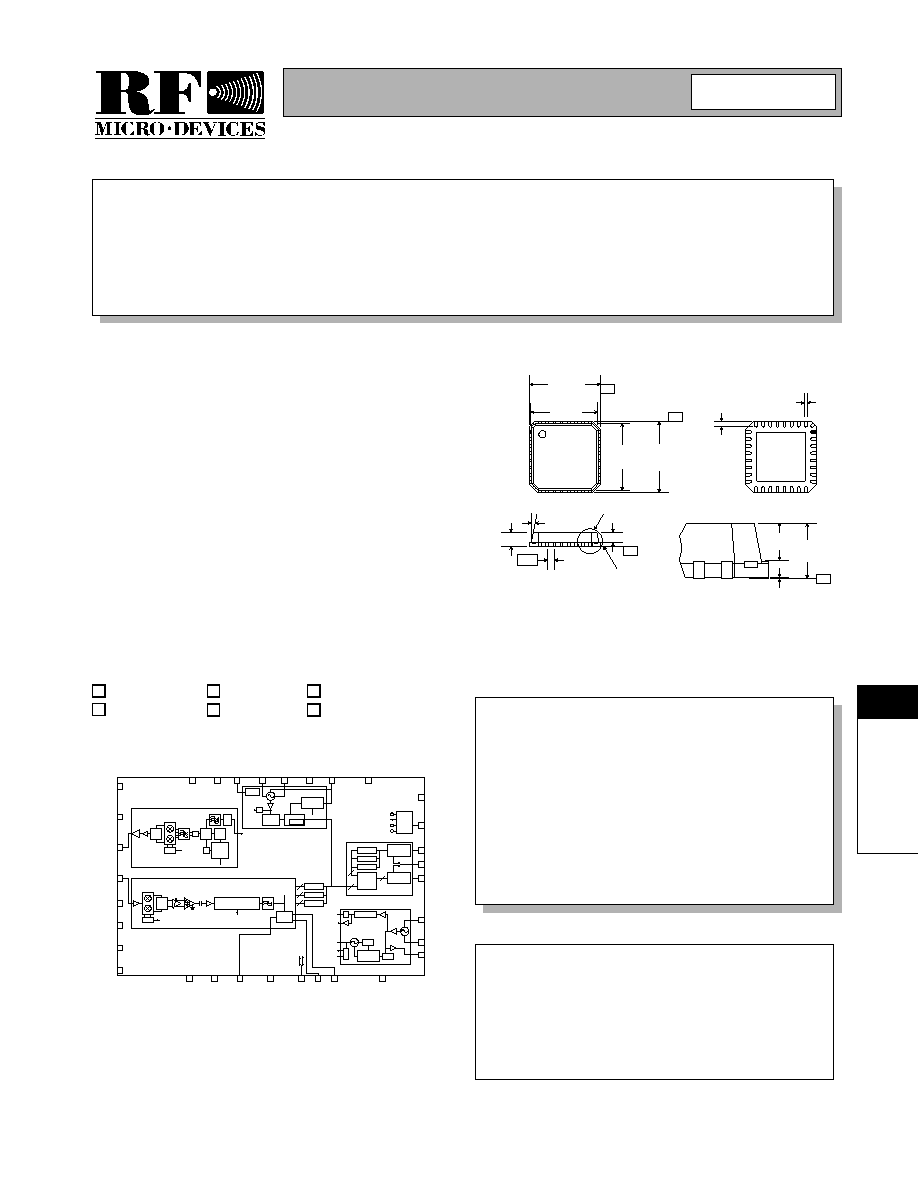
Functional Block Diagram
RF Micro Devices, Inc.
7628 Thorndike Road
Greensboro, NC 27409, USA
Tel (336) 664 1233
Fax (336) 664 0454
http://www.rfmd.com
Optimum Technology Matching� Applied
Si BJT
GaAs MESFET
GaAs HBT
Si Bi-CMOS
�
SiGe HBT
Si CMOS
31
I
F
DG
ND
29
RE
S
N
T
R
+
28
RE
S
N
T
R
-
27
RS
HUNT
26
DO
25
VC
C
6
32
VC
C
7
30
VR
EG
Voltage
Regulator
LO
VCO
Phase Detector/
Charge Pump
Prescaler
16/17
Synthesizer
Address 7
x2
TX
DATA
SYNC
BT = 0.5
4 MHz
ICO
LOOP
FILTER
/4
1 MHz
Phase
Detector /
Charge
Pump
/4
Filter
APPF
LO
Chip
Control
BDATA1
10 MHz
BPKTCTL
BXTLEN
500 kHz
23 BnPWR
24 PLLGND
22 BDCLK
Address 30
Address 31
Address 3
25-Bit Latch
16-Bit Shift
Register
(Read Only)
25-Bit Shift
Register
(Write Only)
21 BDDATA
DBus
25
5
25
20 BnDEN
7
LPO
6
VCC4
5
VCC3
8
DVDDH
4
RXIN
3
TXOUT
2
VCC2
1
VCC1
APPF
LO
1 MHz IF
Transmitter
60
M
H
z
Clock / Data
Recovery
Receiver
Address 4
Address 5
Address 6
16
16
16
/2
500 kHz
1 MHz
/6
/5
10 MHz
60 MHz
/60
Div R
Phase Detector/
Charge Pump
Div R
Ref. Osc.
19 OSC I
18 OSC O
17 BRCLK
LPF/
Equalizer
9
IR
E
F
10
VC
C
5
11
D1
12
BPK
T
C
T
L
13
BD
A
T
A1
14
RE
CCL
K
15
RE
CDA
T
A
16
BX
T
L
E
N
12 MHz
RX
DA
T
A
TX
D
A
TA
FSK Demodulator
RX
DA
T
A
TX DATA
RF2968
BLUETOOTH
TM
TRANSCEIVER
� Bluetooth GSM/GPRS/EDGE Cellular
Phones
� Bluetooth Wireless LAN
� Cordless Phones
� Battery-Powered Portable Devices
The RF2968 is a monolithic integrated circuit intended for
use as a low-cost FSK transceiver in Bluetooth applica-
tions. The device is provided in 32-lead plastic LPCC
packaging and is designed to provide a fully-functional
FSK transceiver. The chip is intended for Bluetooth appli-
cations in the 2.4GHz to 2.5GHz ISM band. The IF and
demodulation sections of the chip require no external fil-
ters or discriminators. The chip also features an image
reject front end and a fully programmable synthesizer
with integrated oscillator circuitry. Self-calibrating RX and
TX IF circuitry optimizes link performance and eliminates
manufacturing variations.
BLUETOOTH is a trademark owned by the Bluetooth SIG, Inc., and licensed
to RF Micro Devices, Inc.
� Fully Monolithic Integrated Transceiver
� Self-Calibrating Transceiver
� Image Reject Receiver
� Bluetooth and BlueRF compatible
� Supports Reference Clocks to 40MHz
� Smallest Footprint Bluetooth Transceiver
TBD
11
Rev A13 010912
NOTES:
1. Shaded lead indicates Pin 1.
2. Package surface roughness at 1.5
�
m � 0.30.
0.70 �
0.08
5
�
m - 20
�
m
1.00
MAX
Detail A
-C-
1.0
MAX
11� � 1�
(4X)
0.50
0.70 � 0.08
See Detail A
Seating
Plane
-C-
4.75
� 0.10
-B-
0.20
0.40 � 0.10
5.00
� 0.10
4.75
� 0.10
-A-
5.00
� 0.10
Package Style: LCC, 32-Pin, 5x5
Preliminary
11-118
RF2968
Rev A13 010912
11
T
R
A
N
S
C
EI
VE
R
S
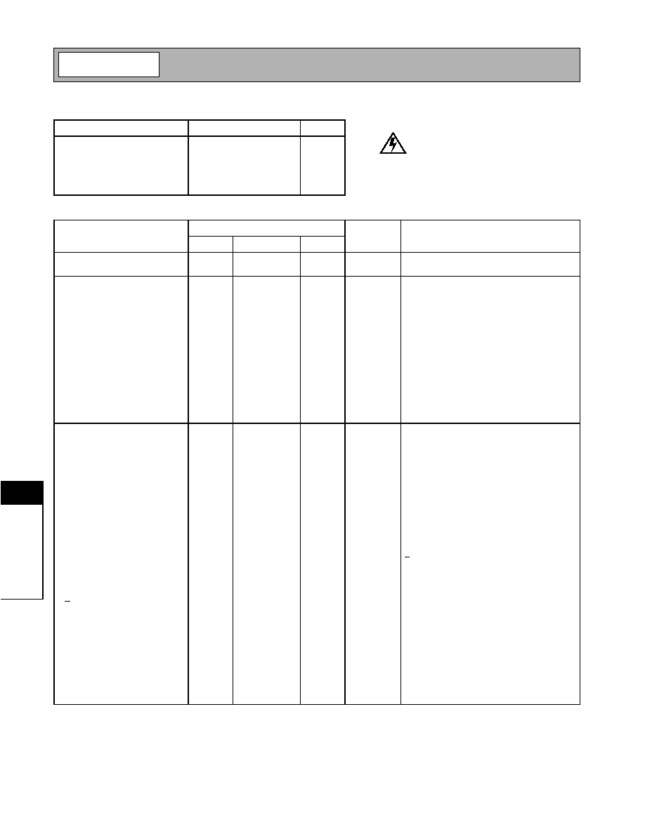
Absolute Maximum Ratings
Parameter
Ratings
Unit
Supply Voltage
-0.5 to +3.6
V
DC
Control Voltages
-0.5 to V
CC
V
DC
Input RF Level
+10
dBm
Operating Ambient Temperature
-40 to +85
�C
Storage Temperature
-55 to +125
�C
Parameter
Specification
Unit
Condition
Min.
Typ.
Max.
Overall
T=25 �C, V
CC
= 3.0V
RF Frequency Range
2400 to 2500
MHz
VCO and PLL Section
VCO Frequency Range
1100 to 1350
MHz
Frequency Tolerance
-50
50
kHz
20ppm crystal; -40�C to +85�C
RF Channels
79
Step Size
1
MHz
Freq= 2.4GHz
SSB Phase Noise
-90
dBc/Hz
Freq= 2.4GHz, 500kHz Offset
-110
dBc/Hz
Freq= 2.4GHz, 2MHz Offset
-124
dBc/Hz
Freq= 2.4GHz, 3MHz Offset
Reference Frequency
10
13
20
MHz
10, 11, 12, 13, 20MHz
20
26
40
MHz
Div2ENB =0; 20, 22, 24, 26, 40MHz.
Hop Time
130
175
�
s
Dual BW =75kHz and 25kHz; BW switch
delay= 100
�
s
K
VCO
85
MHz/V
VCO Freq= 1.2GHz
Transmit Section
Data Rate
1
Mbps
Output Power
0
4
dBm
Power Control Range
28
dB
Power Control Step Size
4
dB
Gain Step Switching Time
4
�
s
From -28dB to 0dB
Output Impedance
25
50
100
VSWR< 2:1
Deviation
140
160
175
kHz
Peak, Data Sequence 00001111
115
kHz
Peak, Data Sequence 01010101
Transmit ISI
Data Sequence 1010
Min Freq Dev, % EYE Open
80
100
%
Reference Data Sequence 00001111
Zero Crossing Error
-125
125
ns
+1/8 Symbol
In-Band Spurious
Measurement BW = 100kHz
Adjacent Channel Power
-20
dBc
Second Channel Power
-20
dBm
>Third Channel Power
-40
dBm
Out-of-Band Spurious
Measurement BW = 100kHz
Operation
-36
dBm
30MHz to 1GHz
-30
dBm
1GHz to 12.75GHz
-47
dBm
1.8GHz to 1.9GHz
-47
dBm
5.15GHz to 5.3GHz
Idle
-57
dBm
30MHz to 1 GHz
-47
dBm
1GHz to 12.75 GHz
-47
dBm
1.8GHz to 1.9GHz
-47
dBm
5.15GHz to 5.3GHz
Caution! ESD sensitive device.
RF Micro Devices believes the furnished information is correct and accurate
at the time of this printing. However, RF Micro Devices reserves the right to
make changes to its products without notice. RF Micro Devices does not
assume responsibility for the use of the described product(s).

Preliminary
11-119
RF2968
Rev A13 010912
11
T
R
A
N
S
C
EI
VE
R
S
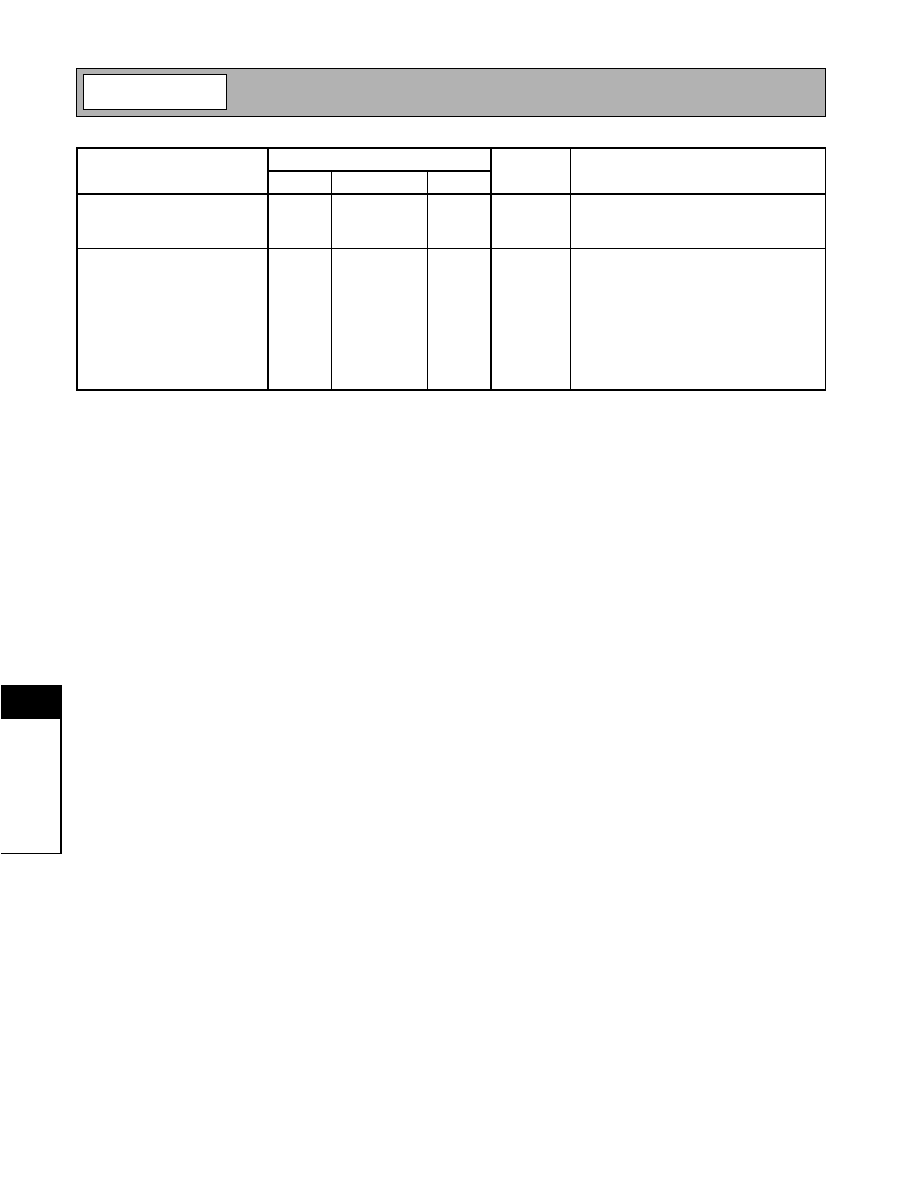
Parameter
Specification
Unit
Condition
Min.
Typ.
Max.
Overall Receive Section
Cascaded Voltage Gain
18
64
dB
Cascaded Noise Figure
8
dB
Cascaded Input IP
3
-14
dBm
RX Sensitivity
-85
dBm
IF BW= 1MHz, BER= 10
-3
Image Rejection
30
dB
RX Input Impedance
25
50
100
2:1 VSWR max.
Interference Performance
BER <10
-3
(C= Desired Signal/I=Interferer)
Co-Channel Interference,
C/I
CO-Channel
14
dB
C= -60dBm
Adjacent (1MHz) Interference,
C/I
1MHz
+4
dB
C= -60dBm
Adjacent (2MHz) Interference,
C/I
2MHz
-30
dB
C= -60dBm
Adjacent (>3MHz) Interfer-
ence, C/I
>3MHz
-40
dB
C= -67dBm
Image Frequency Interfer-
ence, C/I
image
-9
dB
C= -67dBm
Adjacent (1MHz) Interference
to In-Band Image,
C/I
image+1MHz
-20
dB
C= -67dBm
Out-of-Band Blocking
BER <10
-3
, C= -67dBm, tested per evalua-
tion board schematic
Interfering Signal Frequency
30MHz to 2000MHz
-10
dBm
2000MHz to 2400MHz
-27
dBm
2500MHz to 3000MHz
-27
dBm
3000MHz to 12.75GHz
-10
dBm
Intermodulation Characteristic
BER <10
-3
(BT=Bluetooth Modulated Signal)
f1, f2
-39
dBm
f0=-64dBm BT signal
f1=sine
f2=BT signal
|f2- f1| = 3MHz, 4MHz or 5MHz
f0=2f1-f2
Maximum Usable Level
-20
dBm
BER <10
-3
Spurious Emissions
Measurement BW= 100kHz
30MHz to 1GHz
-57
dBm
1GHz to 12.75GHz
-47
dBm
RSSI Operating Range
-80
-20
dBm
Power level at RX IN pin
RSSI Resolution
1
dB
RSSI Absolute Accuracy
-4
4
dB
-60dBm input power
Front End
Voltage Gain
25.5
27.5
29.5
dB
Power Gain
20
dB
Noise Figure
6
8.5
dB
IIP3
-14
dBm
IF Section
IF Frequency
1
MHz
Voltage Gain
-9.5
37
dB
Followed by 1 bit A/D
Noise Figure
25
dB
Preliminary
11-120
RF2968
Rev A13 010912
11
T
R
A
N
S
C
EI
VE
R
S
Parameter
Specification
Unit
Condition
Min.
Typ.
Max.
Data Voltages
Z
LOAD
>10k
Logic Low
0.3
V
Logic High
V
CC
- 0.3
V
Power Supply
Voltage
2.5
3.3
3.6
V
TX Current Consumption
49
mA
Transmit mode, +4dBm output power
RX Current Consumption
49
mA
Receive mode
Sleep Modes
1
�
A
Sleep mode, no low power clock
250
�
A
Sleep mode, low power clock, 12MHz refer-
ence
750
�
A
Sleep mode, low power clock, other refer-
ence
Preliminary
11-121
RF2968
Rev A13 010912
11
T
R
A
N
S
C
EI
VE
R
S
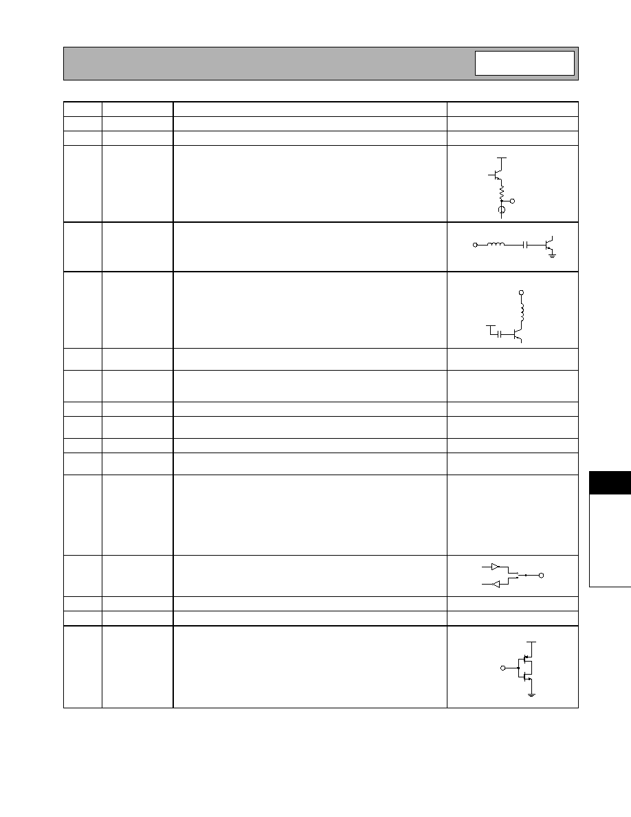
Pin
Function
Description
Interface Schematic
1
VCC1
Supply voltage for the VCO doubler and LO amplifier circuits.
2
VCC2
Supply voltage for the RX mixers, TX PA, and LNA bias circuits.
3
TX OUT
Transmitter output. TX OUT output impedance is 50
(nominal) when
the transmitter is enabled. TX OUT is a high impedance when the
transmitter is disabled. Because this pin is DC-biased, an external cou-
pling capacitor is required.
4
RX IN
Receiver input. RX IN input impedance is a low impedance when the
receiver is enabled. RX IN is a high impedance when the receiver is
disabled. An internal series inductor is used to tune the input imped-
ance.
5
VCC3
Supply voltage for the RX input stage (LNA).
6
VCC4
Supply voltage for the TX mixers and bias circuits of the LO amplifier,
LNA, and RX mixers.
7
LPO
Low frequency clock output for low power mode. In sleep mode, this pin
may provide either a 3.2kHz or 32kHz clock having a 50% duty cycle to
the baseband. In other modes, the output is disabled.
8
DVDDH
Supply voltage for the RX IF VGA circuit.
9
IREF
Connects an external precision resistor (1% tolerance) for generation
of a constant current reference.
10
VCC5
Supply voltage for the analog IF circuits.
11
D1
This is the output of the charge pump for clock recovery circuit. A RC
network from this pin to ground is used to establish the PLL bandwidth.
See pin 26.
12
BPKTCTL
In transmit mode, this pin is used as a strobe to enable the PA stage. In
receive mode, the baseband has the option to use this pin to signal the
detection of the sync word. The baseband drives this pin high at the
end of the sync word, at which time a second DC estimation is per-
formed by sampling the trailer bits. If baseband control is not desired to
signal the second DC estimation, then an internal timer is used to mark
the end of the sync word. The BBC bit is used to select the baseband
control option; the default setting uses the internal timer.
See pin 23.
13
BDATA1
Input data to transmitter/output data from receiver. The input data is
unfiltered data at 1MHz data rate. The pin is bidirectional, switching
between data in and data out modes during Transmit and Receive
modes respectively.
14
RECCLK
Recovered clock output.
See pin 17.
15
RECDATA
Recovered data output.
See pin 17.
16
BXTLEN
This pin is part of the chip power control circuit. It is used to enable/dis-
able "sleep" mode of chip.
TX OUT
10
V
CC
RX IN
V
CC3
VCC3
RXDATA
TX DATA
BDATA1
BXTLEN
V
CC