
11-27
11
T
R
A
N
S
C
EI
VE
R
S
Preliminary
Product Description
Ordering Information
Typical Applications
Features
Functional Block Diagram
RF Micro Devices, Inc.
7625 Thorndike Road
Greensboro, NC 27409, USA
Tel (336) 664 1233
Fax (336) 664 0454
http://www.rfmd.com
Optimum Technology Matching� Applied
Si BJT
GaAs MESFET
GaAs HBT
Si Bi-CMOS
�
SiGe HBT
Si CMOS
Prescaler
32/64
Phase
Detector &
Charge Pump
Lock
Detect
DC
Bias
2
PD
15
OS
C
B
16
OS
C
E
L
OOP
F
L
T
12
RE
S
N
T
R
+
11
RE
S
N
T
R
-
10
3
TX OUT
MOD
I
N
5
13
LD
FLT
14
DIV
C
T
R
L
RF2514
VHF/UHF TRANSMITTER
� 868MHz/915MHz ISM Band Systems
� Local Oscillator Source
� Remote Keyless Entry
� AM/ASK/OOK Transmitter
� Wireless Security Systems
The RF2514 is a monolithic integrated circuit intended for
use as a low-cost AM/ASK transmitter. The device is pro-
vided in a 4 mmx4mm, 16-pin leadless chip carrier and is
designed to provide a phased locked frequency source
for use in local oscillator or transmitter applications. The
chip can be used in applications in the North American
and European VHF /UHF ISM bands. The integrated
VCO, phase detector, reference divider, and reference
oscillator transistor require only the addition of an exter-
nal crystal to provide a complete phase-locked oscillator.
In addition to the standard power-down mode, the chip
also includes an automatic lock detect feature that dis-
ables the transmitter output when the PLL is out-of-lock.
� Fully Integrated PLL Circuit
� Integrated VCO and Reference Oscillator
� 2.2V to 3.6V Supply Voltage
� Low Current and Power Down Capability
� 100MHz to 1000MHz Frequency Range
� Out-of-Lock Inhibit Circuit
RF2514
VHF/UHF Transmitter
RF2514 PCBA
Fully Assembled Evaluation Board
11
Rev A2 010215
3.75
3.75
+
1.50 SQ
4.00
4.00
1
0.45
0.28
3.20
1.60
0.75
0.50
12�
INDEX AREA 3
1.00
0.90
0.75
0.65
0.05
0.00
NOTES:
5
Package Warpage: 0.05 max.
4
Pins 1 and 9 are fused.
Shaded Pin is Lead 1.
1
Dimension applies to plated terminal and is measured between
0.10 mm and 0.25 mm from terminal tip.
2
The terminal #1 identifier and terminal numbering convention
shall conform to JESD 95-1 SPP-012. Details of terminal #1
identifier are optional, but must be located within the zone
indicated. The identifier may be either a mold or marked
feature.
3
0.80
TYP
2
1
Dimensions in mm.
Package Style: LCC, 16-Pin, 4x4

Preliminary
11-28
RF2514
Rev A2 010215
11
T
R
A
N
S
C
EI
VE
R
S
Absolute Maximum Ratings
Parameter
Rating
Unit
Supply Voltage
-0.5 to +3.6
V
DC
Power Down Voltage (V
PD
)
-0.5 to V
CC
V
Operating Ambient Temperature
-40 to +85
�C
Storage Temperature
-40 to +150
�C
Parameter
Specification
Unit
Condition
Min.
Typ.
Max.
Overall
T = 25�C, V
CC
= 3.0V, Freq=916MHz,
R
MODIN
= 10k
Frequency Range
100
868/915
1000
MHz
Modulation
AM/ASK
Modulation Frequency
4
20
kHz
Square wave, 50% duty cycle, 300kHz loop
bandwidth
Incidental FM
15
kHz
P-P
Output Power
1
dBm
50
load, CW
ON/OFF Ratio
52
dB
PLL and Prescaler
Prescaler Divide Ratio
32/64
VCO Gain, K
VCO
40
MHz/V
Frequency and board layout dependent
PLL Phase Noise
-90
dBc/Hz
10kHz Offset, 300kHz loop bandwidth
-95
dBc/Hz
100kHz Offset, 300kHz loop bandwidth
Harmonics
-25
dBc
With matched output and no additional filter-
ing.
Reference Frequency
14.318
17
MHz
Crystal Frequency Spurs
-52
dBc
300kHz PLL loop bandwidth
Max Crystal R
S
10
50
For a typ. 2ms turn-on time.
Max Crystal Motional Inductance
10
mH
For a typ. 2ms turn-on time.
Charge Pump Current
100
�
A
KPD= 100
�
A/2
= 0.0159
�
A/rad
Power Down Control
Power Down (V
IL
)
0
0.3
V
Voltage supplied to the input; device is "OFF"
Power Down (V
IH
)
V
CC
- 0.3
V
CC
V
Voltage supplied to the input; device is "ON"
Control Input Impedance
100
k
Turn On Time
2
ms
Crystal start-up, 14.318MHz crystal.
Turn Off Time
2
ms
Power Supply
Voltage
2.2
3.0
3.6
V
Specifications
Operating limits
Current Consumption
Average
8
mA
50% Duty Cycle 4kHz Data applied to the
MOD IN input. R
MODIN
(R7+ R8) =10k
. Out-
put power/DC current consumption exter-
nally adjustable by modulation input resistor
(see applicable Application Schematic).
Sleep Mode
1
�
A
PD= 0
Caution! ESD sensitive device.
RF Micro Devices believes the furnished information is correct and accurate
at the time of this printing. However, RF Micro Devices reserves the right to
make changes to its products without notice. RF Micro Devices does not
assume responsibility for the use of the described product(s).

Preliminary
11-29
RF2514
Rev A2 010215
11
T
R
A
N
S
C
EI
VE
R
S
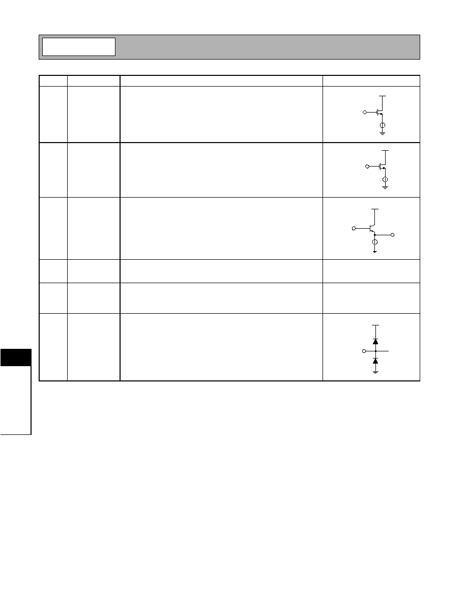
Pin
Function
Description
Interface Schematic
1
GND1
Ground connection for the analog circuits, including TX buffer and out-
put amplifier. Internally connected to die flag. For best performance,
keep traces physically short and connect immediately to ground plane.
2
PD
Power Down control for all circuitry. When this pin is a logic "low" all cir-
cuits are turned off. When this pin is a logic "high", all circuits are oper-
ating normally. See electrical parameters for "high" and "low"
thresholds.
3
TXOUT
Transmitter output. This output is an open collector and requires a pull-
up inductor for bias/matching and a tapped capacitor for matching.
4
VCC1
This pin is used to supply bias to the TX buffer amplifier.
5
MOD IN
AM analog or digital modulation can be imparted to the carrier by an
input to this pin. An external resistor is used to bias the output amplifi-
ers through this pin. The voltage at this pin must not exceed 1.1V.
Higher voltages may damage the device.
See pin 3.
6
VCC2
This pin is used to supply DC bias to the VCO, crystal oscillator, pre-
scaler, phase detector, and charge pump. An IF bypass capacitor
should be connected directly to this pin and returned to ground.
7
GND2
Digital PLL ground connection.
8
VREF P
Bias voltage reference pin for bypassing the prescaler and phase
detector. The bypass capacitor should be of appropriate size to provide
filtering of the reference crystal frequency and be connected directly to
this pin.
9
GND3
See pin 1.
10
RESNTR-
The RESNTR pins are used to supply DC voltage to the VCO, as well
as to tune the center frequency of the VCO. Equal value inductors
should be connected to this pin and pin 11.
11
RESNTR+
See pin 10.
12
LOOP FLT
Output of the charge pump. An RC network from this pin to ground is
used to establish the PLL bandwidth.
V
CC
PD
TX OUT
MOD IN
RF IN
VREFP
V
CC
RESNTR-
RESNTR+
LOOP FLT
4 k
LOOP FLT
V
CC
Preliminary
11-30
RF2514
Rev A2 010215
11
T
R
A
N
S
C
EI
VE
R
S
Pin
Function
Description
Interface Schematic
13
LD FLT
This pin is used to set the threshold of the lock detect circuit. A shunt
capacitor should be used to set an RC time constant with the on-chip
series 1k resistor. The time constant should be approximately 10 times
the reference period.
14
DIV CTRL
Logic "High" input selects divide-by-64 prescaler. Logic "Low" input
selects divide-by-32 prescaler.s
15
OSC B
This pin is connected directly to the reference oscillator transistor base.
The intended reference oscillator configuration is a modified Colpitts. A
68pF capacitor should be connected between pin 15 and pin 16.
16
OSC E
This pin is connected directly to the emitter of the reference oscillator
transistor. A 33pF capacitor should be connected from this pin to
ground.
See pin 15.
Die
Flag
GND
Exposed die flag is centered and measures 1.5mm x1.5mm
(0.059in.x0.059in.). For best results, provide a solder pad for the flag
and connect immediately to ground plane (see evaluation board lay-
out). Internally connected to pins 1 and 9.
ESD
This diode structure is used to provide electrostatic discharge protec-
tion to 3kV using the Human body model. The following pins are pro-
tected: 1, 2, 4-9, 12-14. The die flag is not protected.
LD FLT
V
CC
DIV CTRL
V
CC
OSC E
V
CC
OSC B
V
CC

Preliminary
11-31
RF2514
Rev A2 010215
11
T
R
A
N
S
C
EI
VE
R
S
RF2514 Theory of Operation
Introduction
Short range radio devices are becoming commonplace
in today's environment. The most common examples
are the remote keyless entry systems popular on many
new cars and trucks and the ubiquitous garage door
opener. Other applications are emerging along with the
growth in home security and automation and the
advent of various remote control applications. Typically
these devices have been simplex, or one way, links.
They are also typically built using surface acoustic
wave (SAW) devices as the frequency control ele-
ments. This approach has been attractive because the
SAW devices have been readily available and a trans-
mitter, for example, could be built with only a few addi-
tional components. Recently, however, RF Micro
Devices has introduced several new components that
enable a new class of short range radio devices based
on the use of crystals and phase locked loops for fre-
quency control. These devices are superior in perfor-
mance and comparable in cost to the traditional SAW
based designs. The RF2514 is an example of such a
device. The RF2514 is targeted for applications such
as 315, 433, 868 and 915MHz band remote keyless
entry systems, wireless security systems, and other
remote control applications.
The RF2514 Transmitter
The RF2514 is a low cost AM/ASK VHF/UHF transmit-
ter designed for applications operating within the fre-
quency range of 100MHz to 1000MHz. In particular, it
is intended for 868 and 915MHz band systems (ETS
300 220 applications and FCC Parts 15.231 and
15.249 transmitters) and remote keyless entry sys-
tems. It can also be used as a local oscillator signal
source. The integrated VCO, phase detector, pres-
caler, and reference oscillator require only the addition
of an external crystal to provide a complete phase-
locked loop. In addition to the standard power down
mode, the chip also includes an automatic lock detect
feature that disables the transmitter output when the
PLL is out-of-lock.
The device is manufactured on a 25GHz silicon bipo-
lar-CMOS process and packaged in an industry stan-
dard MLF16 plastic package. This, combined with the
low external parts count, enables the designer to
achieve small-footprint, high-performance, low-cost
designs.
The RF2514 is designed to operate from a supply volt-
age ranging from 2.2V to 3.6V, accommodating
designs using three NiCd battery cells, two AAA flash-
light cells, or a lithium button battery. The device is
capable of providing up to +5dBm output power into a
50
load and is intended to comply with FCC and
ETSI requirements for unlicensed remote control trans-
mitters. ESD protection is provided on all pins except
for OSCB, OSCE, RESNTR-, RESNTR+, TXOUT, and
the two analog ground pins (1 and 9).
While this device is intended for OOK operation, it is
possible to use narrowband FM. This is accomplished
by modulating the reference oscillator rather than
applying the data to the MOD IN input pin. The MOD
IN pin should be tied high to cause the device to trans-
mit. The deviation will be set by pulling limits of the
crystal. Deviation sufficient for the transmission of
voice and other low data rate signals can therefore be
accomplished. Refer to the Application Schematic in
the data sheet for details.
RF2514 Functional Blocks
A PLL consists of a reference oscillator, a phase detec-
tor, a loop filter, a voltage controlled oscillator (VCO),
and a programmable divider in the feedback path. The
RF2514 includes all of these internally except for the
loop filter and the reference oscillator's crystal and two
feedback capacitors.
The reference oscillator is a Colpitts type oscillator.
Pins OSC B and OSC E provide connections to a tran-
sistor that is used as the reference oscillator. The Col-
pitts configuration is a low parts count topology with
reliable performance and reasonable phase noise.
Alternatively, an external signal could be injected into
the base of the transistor. The drive level should, in
either case, be around 500mV
PP
. This level prevents
overdriving the device and keeps the phase noise and
reference spurs to a minimum.
The prescaler uses a series of flip-flops to divide the
VCO frequency by either 64 or 32, depending upon the
logic level present at the DIV CTRL pin. A high logic
level will select the 64 divisor. A low logic level will
select the 32 divisor. This divided signal is then fed into
the phase detector where it is compared with the refer-
ence frequency.
The RF2514 contains an onboard phase detector and
charge pump. The phase detector compares the phase
of the reference oscillator to the phase of the prescaler
output. The phase detector is implemented using flip-
flops in a topology referred to as either "digital phase/
frequency detector" or "digital tri-state comparator".