 | –≠–ª–µ–∫—Ç—Ä–æ–Ω–Ω—ã–π –∫–æ–º–ø–æ–Ω–µ–Ω—Ç: PLUS153B | –°–∫–∞—á–∞—Ç—å:  PDF PDF  ZIP ZIP |
Document Outline
- DESCRIPTION
- FEATURES
- APPLICATIONS
- PIN CONFIGURATIONS
- ORDERING INFORMATION
- LOGIC DIAGRAM
- FUNCTIONAL DIAGRAM
- ABSOLUTE MAXIMUM RATINGS
- THERMAL RATINGS
- DC ELECTRICAL CHARACTERISTICS
- AC ELECTRICAL CHARACTERISTICS
- VOLTAGE WAVEFORMS
- TEST LOAD CIRCUIT
- TIMING DEFINITIONS
- TIMING DIAGRAM
- LOGIC PROGRAMMING
- PROGRAMMING AND SOFTWARE SUPPORT
- OUTPUT POLARITY Ö (B)
- AND ARRAY Ö (I, B)
- OR ARRAY Ö (B)
- VIRGIN STATE
- PROGRAM TABLE
- SNAP RESOURCE SUMMARY DESIGNATIONS

Philips Semiconductors Programmable Logic Devices
Product specification
PLUS153B/D
Programmable logic arrays
(18
◊
42
◊
10)
9
October 22, 1993
853≠1285 11164
DESCRIPTION
The PLUS153 PLDs are high speed,
combinatorial Programmable Logic Arrays.
The Philips Semiconductors state-of-the-art
Oxide Isolated Bipolar fabrication process is
employed to produce propagation delays as
short as 12ns.
The 20-pin PLUS153 devices have a
programmable AND array and a
programmable OR array. Unlike PAL
Æ
devices, 100% product term sharing is
supported. Any of the 32 logic product terms
can be connected to any or all of the 10
output OR gates. Most PAL ICs are limited to
7 AND terms per OR function; the PLUS153
devices can support up to 32 input wide OR
functions.
The polarity of each output is
user-programmable as either active-High or
active-Low, thus allowing AND-OR or
AND-NOR logic implementation. This feature
adds an element of design flexibility,
particularly when implementing complex
decoding functions.
The PLUS153 devices are
user-programmable using one of several
commercially available, industry standard
PLD programmers.
FEATURES
∑
I/O propagation delays (worst case)
≠ PLUS153B ≠ 15ns max.
≠ PLUS153D ≠ 12ns max.
∑
Functional superset of 16L8 and most
other 20-pin combinatorial PAL devices
∑
Two programmable arrays
≠ Supports 32 input wide OR functions
∑
8 inputs
∑
10 bi-directional I/O
∑
42 AND gates
≠ 32 logic product terms
≠ 10 direction control terms
∑
Programmable output polarity
≠ Active-High or Active-Low
∑
Security fuse
∑
3-State outputs
∑
Power dissipation: 750mW (typ.)
∑
TTL Compatible
APPLICATIONS
∑
Random logic
∑
Code converters
∑
Fault detectors
∑
Function generators
∑
Address mapping
∑
Multiplexing
PIN CONFIGURATIONS
1
2
3
4
5
6
7
8
9
10
11
12
13
14
15
16
17
18
19
20
N Package
I0
I1
I2
I3
I4
I5
I6
I7
B0
B2
GND
B3
B4
B5
B6
B7
B8
B9
VCC
B1
1
2
3
4
5
6
7
8
9
10
11
12
13
14
15
16
17
18
19
20
A Package
N = Plastic Dual In-Line Package (300mil-wide)
A = Plastic Leaded Chip Carrier
B4
B5
B6
B7
B8
B2 B3
B1
B0 GND
I3
I4
I5
I6
I7
I1
I2
B9
VCC
I0
ORDERING INFORMATION
DESCRIPTION
t
PD
(MAX)
ORDER CODE
DRAWING NUMBER
20-Pin Plastic Dual-In-Line 300mil-wide
15ns
PLUS153BN
0408D
20-Pin Plastic Dual-In-Line 300mil-wide
12ns
PLUS153DN
0408D
20-Pin Plastic Leaded Chip Carrier
15ns
PLUS153BA
0400E
20-Pin Plastic Leaded Chip Carrier
12ns
PLUS153DA
0400E
Æ
PAL is a registered trademark of Monolithic Memories, Inc., a wholly owned subsidiary of Advanced Micro Devices Corporation.

Philips Semiconductors Programmable Logic Devices
Product specification
PLUS153B/D
Programmable logic arrays
(18
◊
42
◊
10)
October 22, 1993
10
LOGIC DIAGRAM
NOTES:
1. All programmed `AND' gate locations are pulled to logic "1".
2. All programmed `OR' gate locations are pulled to logic "0".
3.
Programmable connection.
(LOGIC TERMS≠P)
(CONTROL TERMS)
1
2
3
4
5
6
7
8
9
11
12
13
14
15
16
17
18
19
I0
I1
I2
I3
I4
I5
I6
I7
B9
B8
B7
B6
B5
B4
B3
B2
B1
B0
31
24 23
16 15
8 7
0
D9D8 D7 D6 D5 D4 D3 D2 D1 D0
S9
S8
S7
S6
S5
S4
S3
S2
S1
S0
X9
X8
X7
X6
X5
X4
X3
X2
X1
X0
B9
B8
B7
B6
B5
B4
B3
B2
B1
B0

Philips Semiconductors Programmable Logic Devices
Product specification
PLUS153B/D
Programmable logic arrays
(18
◊
42
◊
10)
October 22, 1993
11
FUNCTIONAL DIAGRAM
P31
P0
D0
D9
I0
I7
B0
B9
B9
B0
S0
S9
X9
X0
ABSOLUTE MAXIMUM RATINGS
1
THERMAL RATINGS
RATING
SYMBOL
PARAMETER
MIN
MAX
UNIT
V
CC
Supply voltage
+7
V
DC
V
IN
Input voltage
+5.5
V
DC
V
OUT
Output voltage
+5.5
V
DC
I
IN
Input currents
≠30
+30
mA
I
OUT
Output currents
+100
mA
T
amb
Operating free-air temperature range
0
+75
∞
C
T
stg
Storage temperature range
≠65
+150
∞
C
NOTES:
1. Stresses above those listed may cause malfunction or permanent damage to the device.
This is a stress rating only. Functional operation at these or any other condition above
those indicated in the operational and programming specification of the device is not
implied.
TEMPERATURE
Maximum junction
150
∞
C
Maximum ambient
75
∞
C
Allowable thermal rise
75
∞
C
ambient to junction

Philips Semiconductors Programmable Logic Devices
Product specification
PLUS153B/D
Programmable logic arrays
(18
◊
42
◊
10)
October 22, 1993
12
DC ELECTRICAL CHARACTERISTICS
0
∞
C
T
amb
+75
∞
C, 4.75
V
CC
5.25V
LIMITS
SYMBOL
PARAMETER
TEST CONDITIONS
MIN
TYP
1
MAX
UNIT
Input voltage
2
V
IL
Low
V
CC
= MIN
0.8
V
V
IH
High
V
CC
= MAX
2.0
V
V
IC
Clamp
V
CC
= MIN, I
IN
= ≠12mA
≠0.8
≠1.2
V
Output voltage
2
V
CC
= MIN
V
OL
Low
4
I
OL
= 15mA
0.5
V
V
OH
High
5
I
OH
= ≠2mA
2.4
V
Input current
9
V
CC
= MAX
I
IL
Low
V
IN
= 0.45V
≠100
µ
A
I
IH
High
V
IN
= V
CC
40
µ
A
Output current
V
CC
= MAX
I
O(OFF)
Hi-Z state
8
V
OUT
= 2.7V
80
µ
A
V
OUT
= 0.45V
≠140
I
OS
Short circuit
3, 5, 6
V
OUT
= 0V
≠15
≠70
mA
I
CC
V
CC
supply current
7
V
CC
= MAX
150
200
mA
Capacitance
V
CC
= 5V
C
IN
Input
V
IN
= 2.0V
8
pF
C
B
I/O
V
B
= 2.0V
15
pF
NOTES:
1. All typical values are at V
CC
= 5V, T
amb
= +25
∞
C.
2. All voltage values are with respect to network ground terminal.
3. Test one at a time.
4. Measured with inputs I0 ≠ I2 = 0V, inputs I3 ≠ I5 = 4.5V, inputs I7 = 4.5V and I6 = 10V. For outputs B0 ≠ B4 and for outputs B5 ≠ B9 apply the
same conditions except I7 = 0V.
5. Same conditions as Note 4 except I7 = +10V.
6. Duration of short circuit should not exceed 1 second.
7. I
CC
is measured with inputs I0 ≠ I7 and B0 ≠ B9 = 0V.
8. Leakage values are a combination of input and output leakage.
9. I
IL
and I
IH
limits are for dedicated inputs only (I0 ≠ I7).
Philips Semiconductors Programmable Logic Devices
Product specification
PLUS153B/D
Programmable logic arrays
(18
◊
42
◊
10)
October 22, 1993
13
AC ELECTRICAL CHARACTERISTICS
0
∞
C
T
amb
+75
∞
C, 4.75V
V
CC
5.25V, R
1
= 300
, R
2
= 390
LIMITS
SYMBOL
PARAMETER
FROM
TO
TEST
PLUS153B
PLUS153D
UNIT
CONDITION
MIN
TYP
MAX
MIN
TYP
MAX
t
PD
Propagation Delay
2
Input +/≠
Output +/≠
C
L
= 30pF
11
15
10
12
ns
t
OE
Output Enable
1
Input +/≠
Output ≠
C
L
= 30pF
11
15
10
12
ns
t
OD
Output Disable
1
Input +/≠
Output +
C
L
= 5pF
11
15
10
12
ns
NOTES:
1. For 3-State output; output enable times are tested with C
L
= 30pF to the 1.5V level, and S
1
is open for high-impedance to High tests and
closed for high-impedance to Low tests. Output disable times are tested with C
L
= 5pF. High-to-High impedance tests are made to an output
voltage of V
T
= (V
OH
≠ 0.5V) with S
1
open, and Low-to-High impedance tests are made to the V
T
= (V
OL
+ 0.5V) level with S
1
closed.
2. All propagation delays are measured and specified under worst case conditions.
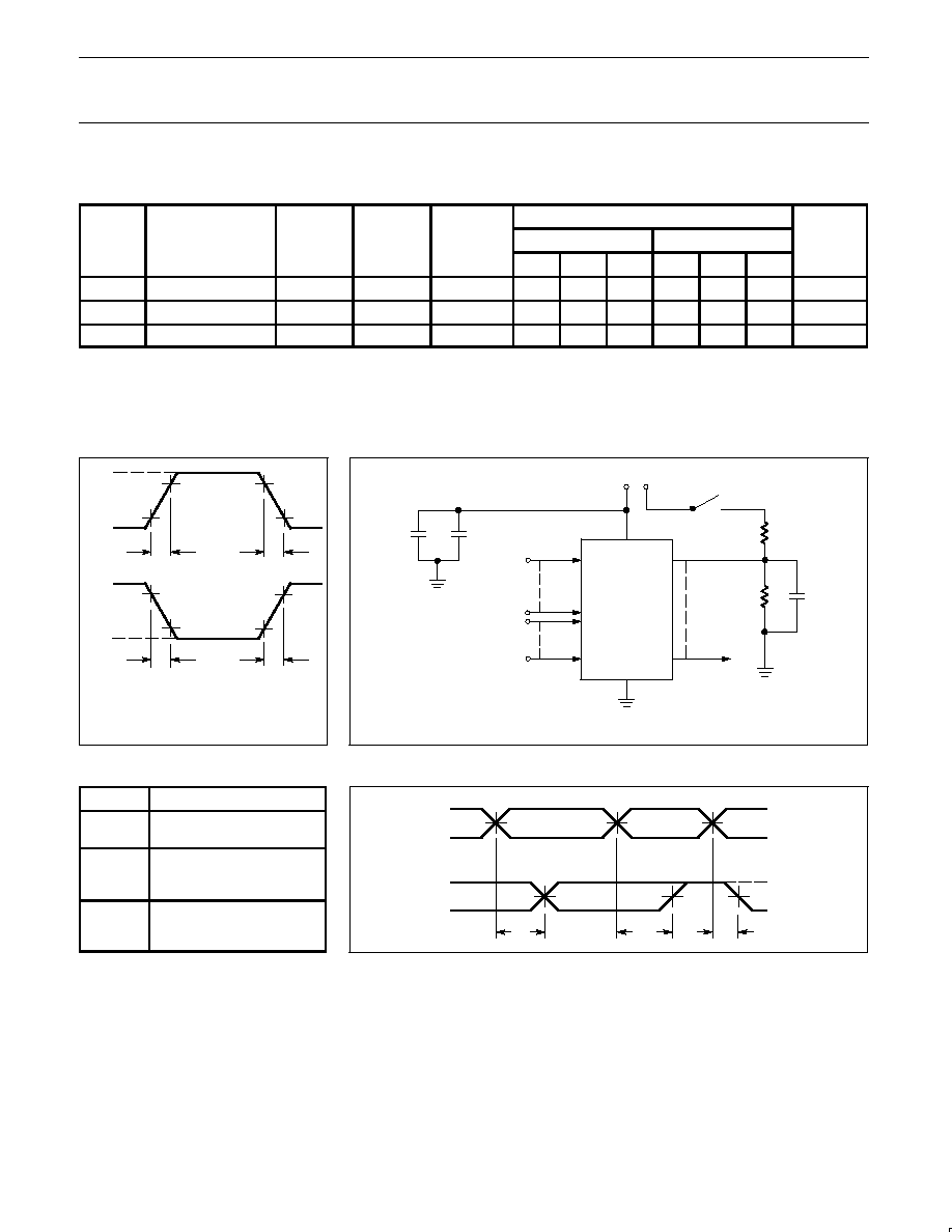
VOLTAGE WAVEFORMS
MEASUREMENTS:
All circuit delays are measured at the +1.5V level
of inputs and outputs, unless otherwise specified.
90%
10%
5ns
5ns
5ns
5ns
90%
10%
+3.0V
+3.0V
0V
0V
tR
tF
Input Pulses
TIMING DEFINITIONS
SYMBOL
PARAMETER
t
PD
Propagation delay between
input and output.
t
OD
Delay between input change
and when output is off (Hi-Z
or High).
t
OE
Delay between input change
and when output reflects
specified output level.
TEST LOAD CIRCUIT
TIMING DIAGRAM
+5V
CL
R1
R2
S1
GND
BZ
BY
INPUTS
I0
I7
BW
BX
OUTPUTS
C2
C1
DUT
NOTE:
C1 and C2 are to bypass VCC to GND.
VCC
+3V
0V
VOH
VOL
I, B
B
tPD
1.5V
1.5V
1.5V
1.5V
1.5V
tOD
tOE
VT

Philips Semiconductors Programmable Logic Devices
Product specification
PLUS153B/D
Programmable logic arrays
(18
◊
42
◊
10)
October 22, 1993
14
LOGIC PROGRAMMING
The PLUS153B/D is fully supported by
industry standard (JEDEC compatible) PLD
CAD tools, including Philips Semiconductors
SNAP design software package. ABEL
TM
and
CUPL
TM
design software packages also
support the PLUS153B/D architecture.
All packages allow Boolean and state
equation entry formats. SNAP, ABEL and
CUPL also accept, as input, schematic
capture format.
PLUS153B/D logic designs can also be
generated using the program table entry
format, which is detailed on the following
page. This program table entry format is
supported by SNAP only.
To implement the desired logic functions, the
state of each logic variable from logic
equations (I, B, O, P, etc.) is assigned a
symbol. The symbols for TRUE,
COMPLEMENT, INACTIVE, PRESET, etc.,
are defined below.
PROGRAMMING AND
SOFTWARE SUPPORT
Refer to Section 9
(Development Software)
and Section 10
(Third-Party
Programmer/Software Support) of this data
handbook for additional information.
AND ARRAY ≠ (I, B)
CODE
O
STATE
INACTIVE1,
2
CODE
STATE
CODE
STATE
CODE
STATE
I, B
H
L
≠
P, D
I, B
I, B
I, B
I, B
P, D
I, B
I, B
I, B
P, D
I, B
I, B
I, B
P, D
I, B
I, B
I, B
DON'T CARE
OR ARRAY ≠ (B)
VIRGIN STATE
A factory shipped virgin device contains all
fusible links intact, such that:
1. All outputs are at "H" polarity.
2. All P
n
terms are disabled.
3. All P
n
terms are active on all outputs.
NOTES:
1. This is the initial unprogrammed state of all links.
2. Any gate P
n
will be unconditionally inhibited if both the true and complement of an input (either
I or B) are left intact.
ABEL is a trademark of Data I/O Corp.
CUPL is a trademark of Logical Devices, Inc.
CODE
ACTIVE LEVEL
LOW
(INVERTING)
L
CODE
ACTIVE LEVEL
HIGH1
(NON≠INVERTING)
H
S
X
B
S
X
B
OUTPUT POLARITY ≠ (B)
CODE
INACTIVE
A
CODE
Pn STATUS
ACTIVE1
∑
P
S
Pn STATUS
P
S

Philips Semiconductors Programmable Logic Devices
Product specification
PLUS153B/D
Programmable logic arrays
(18
◊
42
◊
10)
October 22, 1993
15
PROGRAM TABLE
8
POLARITY
1
2
3
4
5
6
7
8
9
10
11
12
13
14
15
16
17
18
19
20
21
22
23
24
25
26
27
28
29
30
31
D9
D8
D7
D6
D5
D4
D3
D2
D1
D0
PIN
T
E
R
M
AND
OR
ACTIVE
INACTIVE
CONTROL
HIGH
LOW
A
INACTIVE
H
L
B(0)
(POL)
DON'T CARE
I, B
I, B
I, B(I)
CUST
OMER NAME
PHILIPS DEVICE #
PROGRAM T
ABLE #
REV
DA
TE
0
H
L
--
V
ARIABLE
NAME
AND
OR
B(0)
7
6
5
4
3
2
1
0
9
8
7
6
5
4
3
2
1
0
9
8
7
6
5
4
3
2
1
0
B(I)
7
6
5
4
3
2
1
19 18 17 16 15 14 13 12 11
9
19 18 17 16 15 14 13 12 11
9
PURCHASE ORDER #
CF(XXXX)
CUST
OMER SYMBOLIZED P
ART #
T
OT
AL
NUMBER OF P
ARTS
I
0
NOTES
In the unprogrammed state:
Output polarity is non≠inverting.
Unused I and B bits in the
AND array should be programmed
Unused product terms in the OR array should be
as Don't Care (≠).
All
AND gates are pulled to a logic "0" (Low).
programmed as INACTIVE (o).

Philips Semiconductors Programmable Logic Devices
Product specification
PLUS153B/D
Programmable logic arrays
(18
◊
42
◊
10)
October 22, 1993
16
SNAP RESOURCE SUMMARY DESIGNATIONS
CAND
P31
P0
D0
D9
I0
I7
B0
B9
B9
B0
S0
S9
X9
X0
DIN153
NIN153
OR
TOUT153
AND
EXOR153
DIN153
NIN153