LPC2114/LPC2124
Single-chip 16/32-bit microcontrollers; 128/256 kB ISP/IAP
Flash with 10-bit ADC
Rev. 03 -- 22 December 2004
Product data
1.
General description
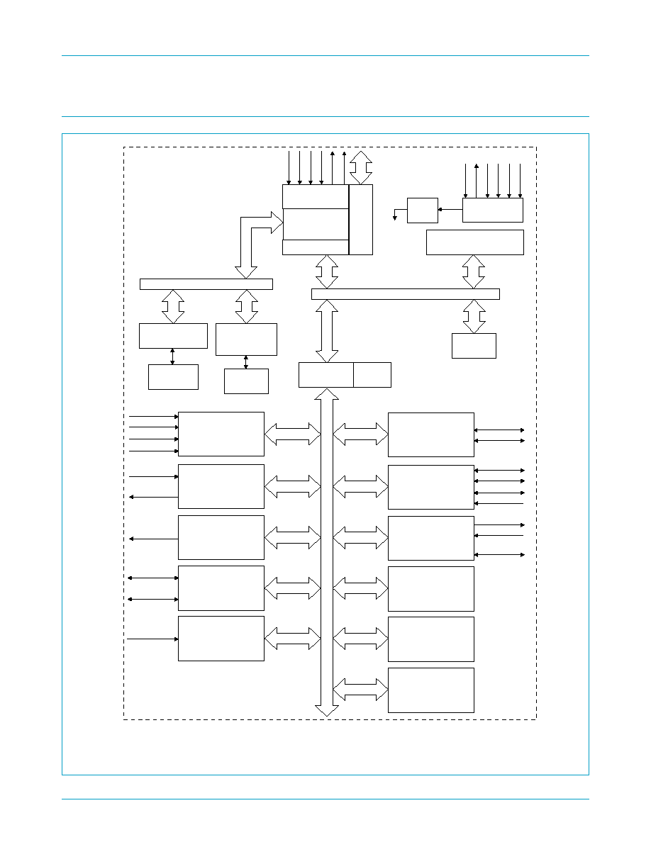
The LPC2114/LPC2124 are based on a 16/32 bit ARM7TDMI-STM CPU with real-time
emulation and embedded trace support, together with 128/256 kilobytes (kB) of
embedded high speed flash memory. A 128-bit wide memory interface and a unique
accelerator architecture enable 32-bit code execution at maximum clock rate. For
critical code size applications, the alternative 16-bit ThumbTM Mode reduces code by
more than 30 % with minimal performance penalty.
With their compact 64 pin package, low power consumption, various 32-bit timers,
4-channel 10-bit ADC, PWM channels and 46 GPIO lines with up to 9 external
interrupt pins these microcontrollers are particularly suitable for industrial control,
medical systems, access control and point-of-sale. With a wide range of serial
communications interfaces, they are also very well suited for communication
gateways, protocol converters and embedded soft modems as well as many other
general-purpose applications.
2.
Features
2.1 Key features
s
16/32-bit ARM7TDMI-S microcontroller in a tiny LQFP64 package.
s
16 kB on-chip Static RAM.
s
128/256 kB on-chip Flash Program Memory. 128-bit wide interface/accelerator
enables high speed 60 MHz operation.
s
In-System Programming (ISP) and In-Application Programming (IAP) via on-chip
boot-loader software. Flash programming takes 1 ms per 512 byte line. Single
sector or full chip erase takes 400 ms.
s
EmbeddedICE-RT interface enables breakpoints and watch points. Interrupt
service routines can continue to execute whilst the foreground task is debugged
with the on-chip RealMonitorTM software.
s
Embedded Trace MacrocellTM enables non-intrusive high speed real-time tracing
of instruction execution.
s
Four channel 10-bit A/D converter with conversion time as low as 2.44
µ
s.
s
Two 32-bit timers (with 4 capture and 4 compare channels), PWM unit (6 outputs),
Real Time Clock and Watchdog.
s
Multiple serial interfaces including two UARTs (16C550), Fast I
2
C (400 kbits/s)
and two SPIsTM.
s
60 MHz maximum CPU clock available from programmable on-chip
Phase-Locked Loop with settling time of 100
µ
s.
s
Vectored Interrupt Controller with configurable priorities and vector addresses.
Philips Semiconductors
LPC2114/LPC2124
Single-chip 16/32-bit microcontrollers
Product data
Rev. 03 -- 22 December 2004
2 of 34
9397 750 13145
© Koninklijke Philips Electronics N.V. 2004. All rights reserved.
s
Up to forty-six 5 V tolerant general purpose I/O pins. Up to nine edge or level
sensitive external interrupt pins available.
s
On-chip crystal oscillator with an operating range of 1 MHz to 30 MHz.
s
Two low power modes, Idle and Power-down.
s
Processor wake-up from Power-down mode via external interrupt.
s
Individual enable/disable of peripheral functions for power optimization.
s
Dual power supply:
x
CPU operating voltage range of 1.65 V to 1.95 V (1.8 V
±
0.15 V).
x
I/O power supply range of 3.0 V to 3.6 V (3.3 V
±
10 %) with 5 V tolerant I/O
pads.16/32-bit ARM7TDMI-S processor.
3.
Ordering information
3.1 Ordering options
Table 1:
Ordering information
Type number
Package
Name
Description
Version
LPC2114FBD64
LQFP64
plastic low profile quad flat package; 64 leads;
body 10
×
10
×
1.4 mm
SOT314-2
LPC2124FBD64
LQFP64
plastic low profile quad flat package; 64 leads;
body 10
×
10
×
1.4 mm
SOT314-2
Table 2:
Part options
Type number
Flash memory
RAM
CAN
Temperature
range (
°
C)
LPC2114FBD64
128 kB
16 kB
-
-
40 to +85
LPC2124FBD64
256 kB
16 kB
-
-
40 to +85

Philips Semiconductors
LPC2114/LPC2124
Single-chip 16/32-bit microcontrollers
Product data
Rev. 03 -- 22 December 2004
5 of 34
9397 750 13145
© Koninklijke Philips Electronics N.V. 2004. All rights reserved.
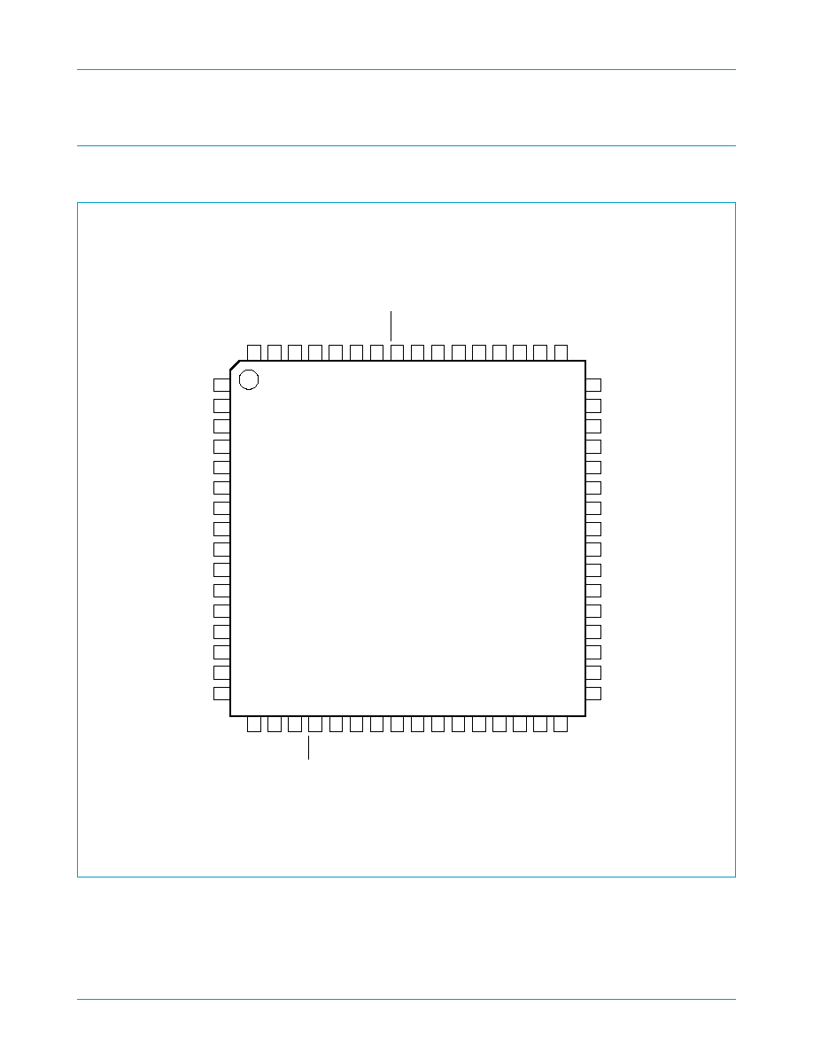
5.2 Pin description
Table 3:
Pin description
Symbol
Pin
Type
Description
P0.0 to P0.31
I/O
Port 0: Port 0 is a 32-bit bi-directional I/O port with individual direction
controls for each bit. The operation of port 0 pins depends upon the pin
function selected via the Pin Connect Block. Pins 26 and 31 of port 0 are not
available.
P0.0
19
O
TxD0 -- Transmitter output for UART0.
O
PWM1 -- Pulse Width Modulator output 1.
P0.1
21
I
RxD0 -- Receiver input for UART0.
O
PWM3 -- Pulse Width Modulator output 3.
I
EINT0 -- External interrupt 0 input
P0.2
22
I/O
SCL -- I
2
C clock input/output. Open drain output (for I
2
C compliance).
I
CAP0.0 -- Capture input for Timer 0, channel 0.
P0.3
26
I/O
SDA -- I
2
C data input/output. Open drain output (for I
2
C compliance).
O
MAT0.0 -- Match output for Timer 0, channel 0.
I
EINT1 -- External interrupt 1 input.
P0.4
27
I/O
SCK0 -- Serial clock for SPI0. SPI clock output from master or input to slave.
I
CAP0.1 -- Capture input for Timer 0, channel 1.
P0.5
29
I/O
MISO0 -- Master In Slave OUT for SPI0. Data input to SPI master or data
output from SPI slave.
O
MAT0.1 -- Match output for Timer 0, channel 1.
P0.6
30
I/O
MOSI0 -- Master Out Slave In for SPI0. Data output from SPI master or data
input to SPI slave.
I
CAP0.2 -- Capture input for Timer 0, channel 2.
P0.7
31
I
SSEL0 -- Slave Select for SPI0. Selects the SPI interface as a slave.
O
PWM2 -- Pulse Width Modulator output 2.
I
EINT2 -- External interrupt 2 input.
P0.8
33
O
TxD1 -- Transmitter output for UART1.
O
PWM4 -- Pulse Width Modulator output 4.
P0.9
34
I
RxD1 -- Receiver input for UART1.
O
PWM6 -- Pulse Width Modulator output 6.
I
EINT3 -- External interrupt 3 input.
P0.10
35
O
RTS1 -- Request to Send output for UART1.
I
CAP1.0 -- Capture input for Timer 1, channel 0.
P0.11
37
I
CTS1 -- Clear to Send input for UART1.
I
CAP1.1 -- Capture input for Timer 1, channel 1.
P0.12
38
I
DSR1 -- Data Set Ready input for UART1.
O
MAT1.0 -- Match output for Timer 1, channel 0.