 | –≠–ª–µ–∫—Ç—Ä–æ–Ω–Ω—ã–π –∫–æ–º–ø–æ–Ω–µ–Ω—Ç: AM6012 | –°–∫–∞—á–∞—Ç—å:  PDF PDF  ZIP ZIP |
Document Outline
- DESCRIPTION
- FEATURES
- PIN CONFIGURATION
- APPLICATIONS
- ORDERING INFORMATION
- BLOCK DIAGRAM
- ABSOLUTE MAXIMUM RATINGS
- DC ELECTRICAL CHARACTERISTICS
- AC ELECTRICAL CHARACTERISTICS
- CIRCUIT DESCRIPTION
- DIFFERENTIAL VS INTEGRAL NONLINEARITY
- DIFFERENTIAL LINEARITY COMPARISON
- ANALOG OUTPUT CURRENTS
- POWER SUPPLIES
- TEMPERATURE PERFORMANCE
- SETTLING TIME
- APPLICATIONS INFORMATION
- Reference Amplifier Setup
- MULTIPLYING OPERATION
- REFERENCE AMPLIFIER COMPENSATION FOR MULTIPLYING APPLICATIONS
- LOGIC INPUTS
- ACCOMMODATING BIPOLAR REFERENCE
- BASIC NEGATIVE REFERENCE OPERATION
- RECOMMENDED FULL-SCALE ADJUSTMENT CIRCUIT
- APPLICATION CIRCUITS
- ADDITIONAL CODE MODIFICATIONS
- APPLICATION CIRCUITS
Philips Semiconductors Linear Products
Product specification
AM6012
12-Bit multiplying D/A converter
776
August 31, 1994
853-0904 13721
DESCRIPTION
The AM6012 12-bit multiplying Digital-to-Analog converter provides
high-speed and 0.025% differential nonlinearity over its full
commercial temperature range.
The D/A converter uses a 3-bit segment generator for the MSBs in
conjunction with a 9-bit R-2R diffused resistor ladder to provide
12-bit resolution without costly trimming processes. This technique
guarantees a very uniform step size (up to
±
LSB from the ideal),
monotonicity to 12 bits and integral nonlinearity to 0.05% at its
differential current outputs.
The dual complementary outputs of the AM6012 increase its
versatility, and effectively double the peak-to-peak output swing.
Digital inputs, in addition, can be configured to accept all popular
logic families.
While the device requires a reference input of 1mA for a 4mA
full-scale current, operation is nearly independent of power supply
voltage shifts. The power supply rejection ratio is
±
0.001% FS/%
V.
The devices will work from +5, -12V to
±
18V rails, with as low as
230mW power consumption typical.
FEATURES
∑
12-bit resolution
∑
Accurate to within
±
0.05%
∑
Monotonic over temperature
∑
Fast settling time, 250ns typical
∑
Trimless design for low cost
∑
Differential current outputs
∑
High-speed multiplying capability
∑
Full-scale current, 4mA (with 1mA reference)
∑
High output compliance voltage, -5 to +10V
∑
Low power consumption, 230mW
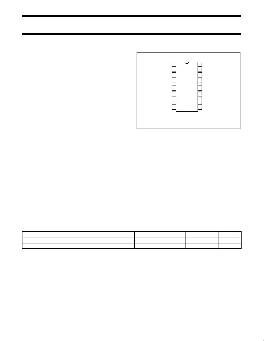
PIN CONFIGURATION
1
2
3
4
5
6
7
8
9
10
11
12
13
14
20
19
18
17
16
15
D
1
and F Packages
NOTE:
1. Available in large SO (SOL) package only.
TOP VIEW
D1
D2
D3
D4
D5
D6
D7
D8
D9
D10
V+
IO
IO
V≠
COMP
VREF(≠)
VREF(+)
GND/VLC
D12 LSB
D11
APPLICATIONS
∑
CRT displays, computer graphics
∑
Robotics and machine tools
∑
Automatic test equipment
∑
Programmable power supplies
∑
CAD/CAM systems
∑
Data acquisition and control systems
∑
Analog-to-digital converter systems
ORDERING INFORMATION
DESCRIPTION
TEMPERATURE RANGE
ORDER CODE
DWG #
20-Pin Ceramic Dual In-Line Package (CERDIP)
0 to +70
∞
C
AM6012F
0584B
20-Pin Plastic Small Outline Large (SOL) Package
0 to +70
∞
C
AM6012D
0172D
Philips Semiconductors Linear Products
Product specification
AM6012
12-Bit multiplying D/A converter
August 31, 1994
777
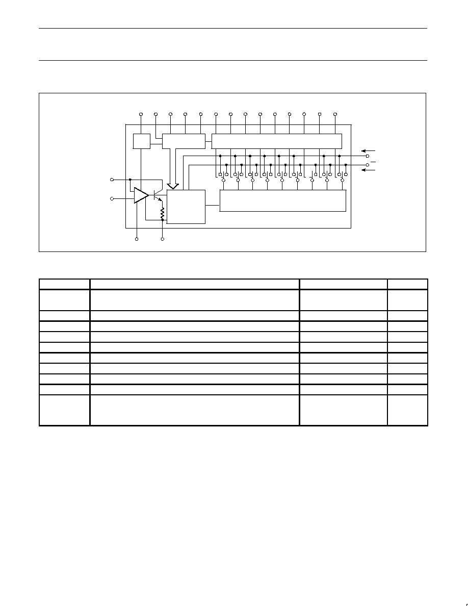
BLOCK DIAGRAM
COMP
V(≠)
16
17
VREF (+)
VREF (≠)
14
15
BIAS
NETWORK
REFERENCE
AMPLIFIER
9-SEGMENT
GENERATOR
DECODER
CURRENT
SWITCHES
ISEG
9-BIT R-2R
D/A CONVERTER
LOGIC SWITCHES
18
19
IO
IO
12
11
10
9
8
7
6
5
4
3
2
1
13
LSB
GND/MSB
20
V(+)
VLC
B12
B11
B10
B9
b8
B7
B6
B5
B4
B3
B2
B1
ABSOLUTE MAXIMUM RATINGS
SYMBOL
PARAMETER
RATING
UNIT
T
A
Operating temperature
AM6012F
0 to +70
∞
C
T
STG
Storage temperature range
-65 to +150
∞
C
T
SOLD
Lead soldering temperature 10sec max
300
∞
C
V
S
Power supply voltage
±
18
V
Logic inputs
-5V to +18
V
Voltage across current outputs
-8V to +12
V
V
REF
Reference inputs V
14
, V
15
V- to V+
V
REF
Reference input differential voltage (V
14
to V
15
)
±
18
V
I
REF
Reference input current (I
14
)
1.25
mA
P
D
Maximum power dissipation, T
A
=25
∞
C, (still-air)
1
F package
1560
mW
D package
1390
mW
NOTES:
1. Derate above 25
∞
C, at the following rate:
F package at 12.5mW/
∞
C
D package at 11.1mW/
∞
C

Philips Semiconductors Linear Products
Product specification
AM6012
12-Bit multiplying D/A converter
August 31, 1994
778
DC ELECTRICAL CHARACTERISTICS
V+=+15V, V-=-15V, I
REF
=1.0mA, 0
∞
C
T
A
70
∞
C
SYMBOL
PARAMETER
TEST CONDITIONS
LIMITS
UNIT
SYMBOL
PARAMETER
TEST CONDITIONS
Min
Typ
Max
UNIT
Resolution
12
Bits
Monotonicity
12
Bits
DNL
Differential nonlinearity
Deviation from ideal step size
±
0.025
%FS
12
Bits
NL
Nonlinearity
Deviation from ideal straight line
±
.05
%FS
I
FS
Full-scale current
V
REF
=10.000V
R
14
-R
15
=10.000k
T
A
=25
∞
C
3.935
3.999
4.063
mA
TCI
FS
Full-scale tempco
±
10
±
40
ppm/
∞
C
±
0.001
±
0.004
%FS/
∞
C
V
OC
Output voltage compliance
DNL Specification guaranteed over
compliance range
R
OUT
>10M
typ.
-5
+10
V
I
FSS
Symmetry
I
FS
-I
FS
±
0.4
±
2.0
µ
A
I
ZS
Zero-scale current
0.10
µ
A
V
IL
V
IH
Logic
input
levels
Logic "0"
0.8
V
Logic "1"
2.0
I
IN
Logic input current
V
IN
=-5 to +18V
40
µ
A
V
IS
Logic input swing
V-=-15V
-5
+18
V
I
REF
Reference current range
0.2
1.0
1.1
mA
I
15
Reference bias current
0
-0.5
-2.0
µ
A
dl/dt
Reference input slew rate
R
14(eq)
=800
C
C
=0pF
4.0
8.0
mA/
µ
s
PSSI
FS+
Power supply sensitivity
V+=+13.5V to +16.5V, V-=-15V
±
0.0005
±
0.001
%FS/%
PSSI
FS-
V-=-13.5V to -16.5V, V+=+15V
±
0.00025
±
0.001
V+
Power supply range
V
OUT
=0V
4.5
18
V
V-
-18
-10.8
I+
V+=+5V, V-=-15V
5.7
8.5
I-
Power supply current
-13.7
-18.0
mA
I+
V+=+15V, V-=-15V
5.7
8.5
I-
-13.7
-18.0
P
D
Power dissipation
V+=+5V, V-=-15V
234
312
mW
V+=+15V, V-=-15V
291
397
AC ELECTRICAL CHARACTERISTICS
V+=+15V, V-=-15V, I
REF
=1.0mA, 0
∞
C
T
A
70
∞
C
SYMBOL
PARAMETER
TEST CONDITIONS
LIMITS
UNIT
SYMBOL
PARAMETER
TEST CONDITIONS
Min
Typ
Max
UNIT
t
S
Settling time
To
±
1/2LSB, all bits ON or OFF, T
A
=25
∞
C
250
500
ns
t
PLH
t
PHL
Propagation
delay--all bits
50% to 50%
25
50
ns
C
OUT
Output capacitance
20
pF

Philips Semiconductors Linear Products
Product specification
AM6012
12-Bit multiplying D/A converter
August 31, 1994
779
CIRCUIT DESCRIPTION
The AM6012 is a 12-bit DAC which uses diffused resistors and
requires no trimming to guarantee monotonicity over the
temperature range. A segmented DAC design guarantees a more
uniform step size over the temperature range than is normally
available with trimmed 12-bit converters. The converter features
differential high compliance current outputs, wide supply range, and
a multiplying reference input.
In many converter applications, uniform step size is more important
than conformance to an ideal straight line. Many 12-bit converters
are used for high resolution rather than high linearity, since few
transducers are more linear than
±
0.1%. All classic binarily weighted
converters require
±
1/2LSB (
±
0.012%) linearity in order to guarantee
monotonicity, which requires very tight resistor matching and
tracking. The AM6012 uses conventional bipolar processing to
achieve high differential linearity and monotonicity without requiring
correspondingly high linearity, or conformance to an ideal straight
line.
One design approach which provides monotonicity without requiring
high linearity is the MOS switch-resistor string. This circuit is actually
a full complement to a current-switched R-2R DAC since it is slower,
has a voltage output, and, if implemented at the 12-bit level, would
use 4096 low tolerance resistors rather than a minimum number of
high tolerance resistors as in the R-2R network. Its lack of speed
and density for 12 bits are its drawbacks.
With the segmented DAC approach, the 4096 required output levels
are composed of 8 groups of 512 steps each. Each step group is
generated by a 9-bit DAC, and each of the segment slopes is
determined by one of 8 equal current sources. The resistors which
determine monotonicity are in the 9-bit DAC. The major carry of the
9-bit DAC is repeated in each of the 8 segments, and requires eight
times lower initial resistor accuracy and tracking to maintain a given
differential nonlinearity over temperature.
The operation of the segmented DAC may be visualized by
assuming an input code of all zeroes. The first segment current I
O
is
divided into 512 levels by the 9-bit multiplying DAC and fed to the
output, I
OUT
. As the input code increases, a new segment current is
selected for each 512 counts. The previous segment is fed to output
I
OUT
where the new step group is added to it, thus ensuring
monotonicity independent of segment resistor values. All higher
order segments feed I
OUT
.
With the segmented DAC approach, the precision of the 8 main
resistors determines linearity only. The influence of each of these
resistors on linearity is four times lower than that of the MSB resistor
in an R-2R DAC. Hence, assuming the same resistor tolerances for
both, the linearity of the segmented approach would actually be
higher than that of an R-2R design.
The step generator or 9-bit DAC is composed of a master and a
slave ladder. The slave ladder generates the four least significant
bits from the remainder of the master ladder by active current
splitting utilizing scaled emitters. This saves ladder resistors and
greatly reduces the range of emitter scaling required in the 9-bit
DAC. All current switches in the step generator are high-speed
fully-differential switches which are capable of switching low currents
at high speed. This allows the use of a binary scaled network all the
way to the least significant bit which saves power and simplifies the
circuitry.
Diffused resistors have advantages over thin film resistors beyond
simple economy and bipolar process compatibility. The resistors are
fabricated in single crystal rather than amorphous material which
gives them better long term stability and tracking and much higher
moisture resistance. They are diffused at 1000
∞
C and so are
resistant to changes in value due to thermal and chemical causes.
Also, no burn-in is required for stability. The contact resistance
between aluminum and silicon is more predictable than between
aluminum and an amorphous thin film, and no sandwich metals are
required to enhance or protect the contact or limit alloying. The initial
match between two diffused resistors is similar to that of thin film
since both are defined by photomasks and chemical etching. Since
the resistors are not trimmed or altered after fabrication, their
tracking and long-term characteristics are not degraded.
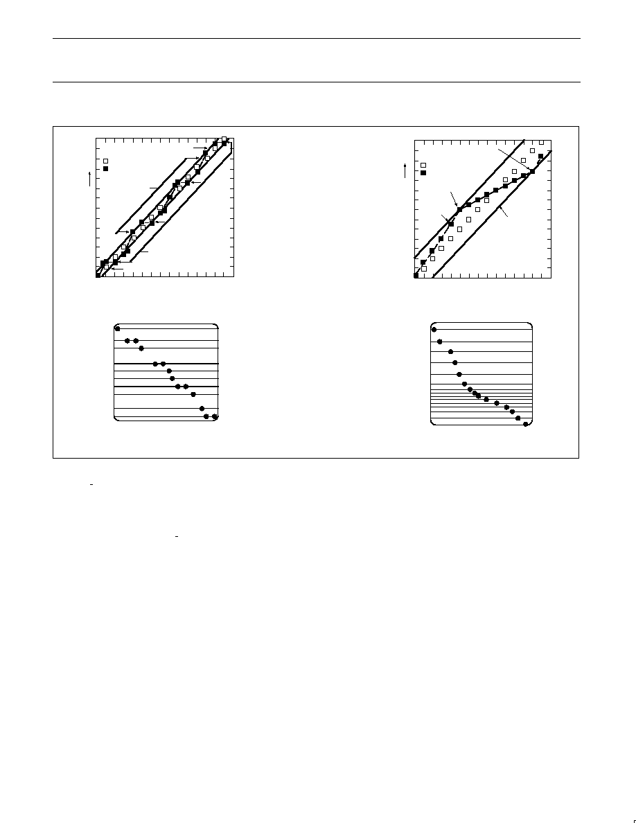
DIFFERENTIAL VS INTEGRAL NONLINEARITY
Integral nonlinearity, for the purposes of the discussion, refers to the
"straightness" of the line drawn through the individual response
points of a data converter. Differential nonlinearity, on the other
hand, refers to the deviation of the spacing of the adjacent points
from a 1 LSB ideal spacing. Both may be expressed as either a
percentage of full-scale output or as fractional LSBs or both. The
graphs in Figure 1 define the manner in which these parameters are
specified. The left graph shows a portion of the transfer curve of a
DAC with 1/2LSB INL and the (implied) DNL spec of 1 LSB. Below
this is a graphic representation of the way this would appear on a
CRT screen where the AM6012 is used as a display driver. On the
right is a portion of the transfer curve of a DAC specified for 1/2LSB
INL with LSB DNL specified and the graphic display below it.
One of the characteristics of an R-2R DAC in standard form is that
any transition which causes a zero LSB change (i.e., the same
output for two different codes) will exhibit the same output each time
that transition occurs. The same holds true for transitions causing a
2 LSB change. These two problem transitions are allowable for the
standard definition of monotonicity and also allow the device to be
specified very tightly for INL. The major problem arising from this
error type is in A/D converter implementations. Inputs producing the
same output are now represented by ambiguous output codes for an
identical input. Also, two LSB gaps can cause large errors at those
input levels (assuming 1/2LSB quantizing levels). It can be seen
from the two figures that the DNL-specified D/A converter will yield
much finer grained data than the INL-specified part, thus improving
the ability of the A/D to resolve changes in the analog input.
Philips Semiconductors Linear Products
Product specification
AM6012
12-Bit multiplying D/A converter
August 31, 1994
780
DIFFERENTIAL LINEARITY COMPARISON
ANALOG OUT
Figure 1. Differential Linearity Comparison
±
1/2LSB INL,
±
1LSB DNL
±
2LSB INL,
±
1LSB DNL
0000 0010
0100 0110 1000 1010 1100 1110
0001 0011
0101 0111 1001 1011 1101 1111
IDEAL OUTPUTS
ACUTAL OUTPUTS
+1/2LSB
LIMIT
2LSB CHANGE ON
X011≠X100
TRANSITION
SEGMENT
OF 12-BIT
DAC TRANSFER
CURVE FOR:
NO CHANGE ON
XX01≠XX10 TRANSITION
≠1/2LSB LIMIT
DIGITAL INPUT
ANALOG OUT
INL =
±
1/2LSB
DNL =
±
1LSB
0010 0010
0100 0110 1000 1010 1100 1110
0001 0011
0101 0111 1001 1011 1101 1111
DNL =
±
2LSB
INL =
±
2LSB
SEGMENT OF 12-BIT DAC
TRANSFER CURVE FOR:
≠2 LSB
LIMIT
SEGMENT
CHANGE
IDEAL OUTPUTS
ACUTAL OUTPUTS
SEGMENT
CHANGE
+2LSB
LIMIT
DIGITAL INPUT
ANALOG OUTPUT CURRENTS
Both true and complemented output sink currents are provided
where I
O
+I
O
=I
FR
. Current appears at the "true" output when a "1" is
applied to each logic input. As the binary count increases, the sink
current at Pin 18 increases proportionally, in the fashion of a
"positive logic" D/A converter. When a "0" is applied to any input bit,
that current is turned off at Pin 18 and turned on at Pin 19. A
decreasing logic count increases I
O
as in a negative or inverted logic
D/A converter. Both outputs may be used simultaneously. If one of
the outputs is not required, it must still be connected to ground or to
a point capable of sourcing I
FR
; do not leave an unused output pin
open.
Both outputs have an extremely wide voltage compliance enabling
fast direct current-to-voltage conversion through a resistor tied to
ground or other voltage source. Positive compliance is 25V above V-
and is independent of the positive supply. Negative compliance is
+10V above V-.
The dual outputs enable double the usual peak-to-peak load swing
when driving loads in quasi-differential fashion. This feature is
especially useful in cable driving, CRT deflection and in other
balanced applications such as driving center-tapped coils and
transformers.
POWER SUPPLIES
The AM6012 operates over a wide range of power supply voltages
from a total supply of 20V to 36V. When operating with V- supplies
of -10V or less, I
REF
1mA is recommended. Low reference current
operation decreases power consumption and increases negative
compliance, reference amplifier negative common-mode range,
negative logic input range, and negative logic threshold range;
consult the various figures for guidance. For example, operation at
-9V with I
REF
=1mA is not recommended because negative output
compliance would be reduced to near zero. Operation from lower
supplies is possible, however at least 8V total must be applied to
insure turn-on of the internal bias network.
Symmetrical supplies are not required, as the AM6012 is quite
insensitive to variations in supply voltage. Battery operation is
feasible as no ground connection is required; however, an artificial
ground may be used to insure logic swings, etc., remain between
acceptable limits.
TEMPERATURE PERFORMANCE
The nonlinearity and monotonicity specifications of the AM6012 are
guaranteed to apply over the entire rated operating temperature
range. Full-scale output current drift is tight, typically
±
10ppm/
∞
C,
with zero-scale output current and drift essentially negligible
compared to 1/2LSB.
The temperature coefficient of the reference resistor R
14
should
match and track that of the output resistor for minimum overall
full-scale drift.
SETTLING TIME
The AM6012 is capable of extremely fast settling times, typically
250ns at I
REF
=1.0mA. Judicious circuit design and careful board
layout must be employed to obtain full performance potential during