Philips Semiconductors
Product data
74ALVCH16832
7-bit to 28-bit address register/driver with 3-state
outputs
2
2001 Dec 14
853-2311 27460
FEATURES
∑
ESD protection exceeds 2000 V HBM per JESD22-A114,
200 V MM per JESD22-A115 and 1000 V CDM per JESD22-C101
∑
Latch-up testing is done to JESDEC Standard JESD78 which
exceeds 100 mA
∑
Bus hold on data inputs eliminates the need for external
pullup/pulldown resistors
DESCRIPTION
This 7 channel 1-bit to 4-bit address register/driver is designed for
2.3 V to 3.6 V V
CC
operation. This device is ideal for use in
applications in which a single address bus is driving four separate
memory locations. The 74ALVCH16832 can be used as a buffer or
a register, depending on the logic level of the select (SEL) input.
When SEL is a logic high, the device is in the buffer mode. The
outputs follow the inputs and are controlled by the two output-enable
(OE) inputs. Each OE controls two groups of seven outputs.
When SEL is a logic low, the device is in the register mode. The
register is an edge-triggered D-type flip-flop. On the positive
transition of the clock (CLK) input, data at the A inputs is stored in
the internal registers. OE operates the same as in the buffer mode.
When OE is a logic low, the outputs are in a normal logic state, (high
or low logic level). When OE is a logic high, the outputs are in the
high-impedance state.
Neither SEL of OE affect the internal operation of the flip-flops. Old
data can be retained or new data can be entered while the outputs
are in the high-impedance state.
To ensure the high-impedance state during power up or power
down, OE should be tied to V
CC
through a pullup resistor; the
minimum value of the resistor is determined by the current-sinking
capability of the driver.
Active buss-hold circuitry is provided to hold unused or floating data
inputs at a valid logic level.
The 74ALVCH16832 is characterized for operation from ≠40 to
+85
∞
C.
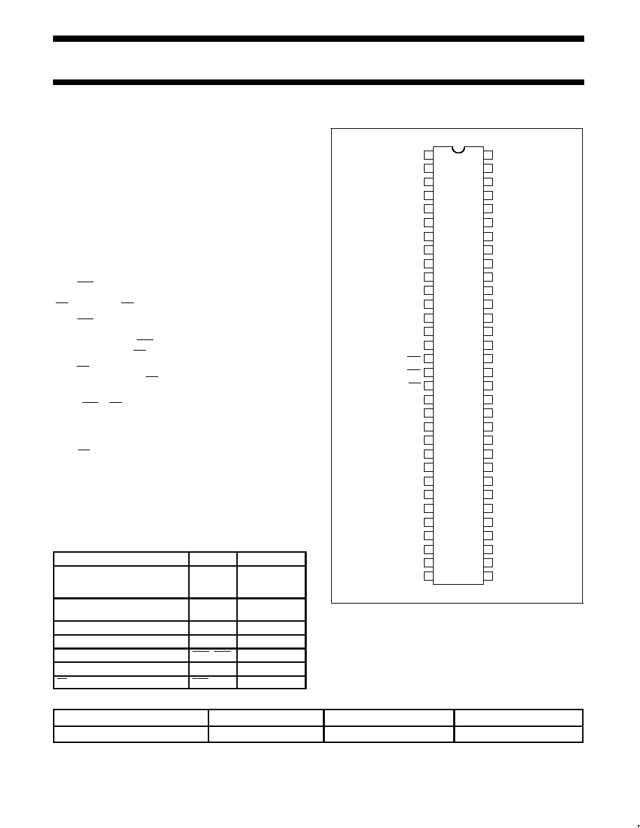
PIN DESCRIPTION
PIN(S)
SYMBOL
FUNCTION
1, 2, 4, 5, 28. 29, 31, 32, 33, 34,
36, 37, 41, 42, 44, 45, 47, 48, 49,
50, 54, 55, 57, 58, 60, 61, 63, 64
1Yn, 2Yn,
3Yn, 4Yn
Outputs
3, 8, 10, 14, 19, 23, 25, 30, 35,
39, 40, 46, 51, 53, 56, 62
GND
Ground
6, 12, 22, 27, 38, 43, 52, 59
V
CC
Supply voltage
7, 9, 11, 20, 21, 24, 26
An
Inputs
16, 17
OE1, OE2
Output enable
15
CLK
Clock
18
SEL
Select
PIN CONFIGURATION
1
2
3
4
5
6
7
8
9
10
11
12
53
54
55
56
57
58
59
60
61
62
63
64
4Y1
GND
2Y1
1Y1
V
CC
A1
GND
A2
GND
A3
1Y2
2Y2
GND
3Y2
4Y2
V
CC
1Y3
GND
2Y3
3Y3
4Y3
GND
V
CC
13
14
15
16
17
18
47
48
49
50
51
52
NC
GND
CLK
OE1
OE2
V
CC
1Y4
GND
2Y4
3Y4
SEL
19
46
4Y4
GND
20
21
22
23
24
25
40
41
42
43
44
45
A4
A5
V
CC
GND
A6
GND
V
CC
1Y5
3Y5
4Y5
GND
GND
26
39 GND
A7
27
38 V
CC
V
CC
28
29
30
31
32
33
34
135
36
37
4Y7
3Y7
GND
2Y7
1Y7
1Y6
GND
3Y6
4Y6
3Y1
2Y6
2Y5
SV01912
ORDERING INFORMATION
PACKAGES
TEMPERATURE RANGE
ORDER CODE
DWG NUMBER
64-pin Plastic TSSOP
≠40 to +85
∞
C
74ALVCH16832DGG
SOT646-1

Philips Semiconductors
Product data
74ALVCH16832
7-bit to 28-bit address register/driver with
3-state outputs
2001 Dec 14
3
LOGIC DIAGRAM (POSITIVE LOGIC)
SV01913
OE2
OE1
5
4
1Y1
2Y1
to 6 other channels
2
1
3Y1
4Y1
CLK
D
Q
CLK
A1
SEL
18
7
15
17
16
FUNCTION TABLE
Inputs
Output
OE
SEL
CLK
A
Y
H
X
X
X
Z
L
H
X
L
L
L
H
X
H
H
L
L
L
L
L
L
H
H
ABSOLUTE MAXIMUM RATINGS
Over recommended operating free-air temperature range (unless otherwise noted).
1
SYMBOL
PARAMETER
CONDITIONS
RATING
UNIT
V
CC
Supply voltage range
≠0.5 to +4.6
V
V
I
Input voltage range
See Note 2
≠0.5 to +4.6
V
V
O
Output voltage range
See Notes 2 and 3
≠0.5 to V
CC
+0.5
V
I
IK
Input clamp current
V
I
< 0
≠50
mA
I
OK
Output clamp current
V
O
< 0
≠50
mA
I
O
Continuous output current
"
50
mA
I
CC
, I
GND
Continuous current through each V
CC
or GND
"
100
mA
JA
Package thermal impedance
See Note 4
106
∞
C/W
T
stg
Storage temperature range
≠65 to +150
∞
C
NOTES:
1. Stresses beyond those listed under "absolute maximum ratings" may cause permanent damage to the device. These are stress ratings
only, and functional operation of the device at these or any other conditions beyond those indicated under "recommended operating
conditions" is not implied. Exposure to absolute-maximum-rated conditions for extended periods may affect device reliability.
2. The input negative-voltage and output voltage ratings may be exceeded if the input and output current ratings are observed.
3. This value is limited to 4.6 V maximum.
4. The package thermal impedance is calculated in accordance with JESD 51.


