 | ÐлекÑÑоннÑй компоненÑ: NB7L216 | СкаÑаÑÑ:  PDF PDF  ZIP ZIP |
NB7L216
©
Semiconductor Components Industries, LLC, 2005
March, 2005 - Rev. 0
1
Publication Order Number:
NB7L216/D
NB7L216
2.5V/3.3V, 12Gb/s Multi
Level Clock/Data Input to
RSECL, High Gain
Receiver/Buffer/Translator
with Internal Termination
The NB7L216 is a differential receiver/driver with high gain output
targeted for high frequency applications. The device is functionally
equivalent to the NBSG16 but with much higher gain output. This
highly versatile device provides 35 dB of gain up to 7 GHz.
Inputs incorporate internal 50
W termination resistors and accept
Negative ECL (NECL), Positive ECL (PECL), LVTTL, LVCMOS,
CML, or LVDS. Outputs are Reduced Swing ECL (RSECL), 400 mV.
The V
BB
pin is internally generated voltage supply available to this
device only. The V
BB
is used as a reference voltage for single-ended
NECL or PECL inputs. For all single-ended input conditions, the
unused complementary differential input should be connected to V
BB
as a switching reference voltage. V
BB
may also rebias AC coupled
inputs. When used, decouple V
BB
via a 0.01
mF capacitor and limit
current sourcing or sinking to 0.5 mA. When not used, V
BB
output
should be left open.
Application notes, models and support documentation are available
at www.onsemi.com.
Features
·
High Gain of 35 dB from DC to 7 GHz Typical
·
High IIP3: 0 dB Typical
·
20 mV Minimum Input Voltage Swing
·
Maximum Input Clock Frequency up to 8.5 GHz
·
Maximum Input Data Rate up to 12 Gb/s Typical
·
<0.5 ps of RMS Clock Jitter
·
<9 ps of Data Dependent Jitter
·
120 ps Typical Propagation Delay
·
30 ps Typical Rise and Fall Times
·
RSPECL Output with Operating Range: V
CC
= 2.375 V to 3.465 V
with V
EE
= 0 V
·
RSNECL Output with RSNECL or NECL Inputs with Operating
Range: V
CC
= 0 V with V
EE
= -2.375 V to -3.465 V
·
RSECL Output Level (400 mV Peak-to-Peak Output),
·
50
W Internal Input Termination Resistors (Temperature-Coefficient
of < 6.38 m
W/
°
C)
·
V
BB
ECL
Reference Voltage Output
·
Pb-Free Packages are Available
QFN-16
MN SUFFIX
CASE 485G
MARKING
DIAGRAM*
*For additional marking information, refer to
Application Note AND8002/D.
A
= Assembly Location
L
= Wafer Lot
Y
= Year
W
= Work Week
See detailed ordering and shipping information in the package
dimensions section on page 11 of this data sheet.
ORDERING INFORMATION
16
NB7L
216
ALYW
1
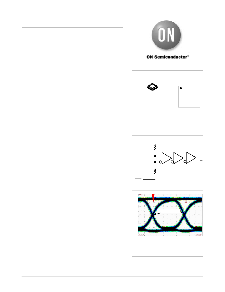
Figure 1. Functional Block Diagram
50
W
50
W
VTD
D
D
VTD
Q
Q
TIME (17 ps/div)
Figure 2. Typical Output Waveform at
12 Gb/s with PRBS 2
23
-1 (V
INPP
= 400 mV,
Input Signal DDJ = 12 ps)
VOL
T
AGE (60 mV/div)
http://onsemi.com
Device DDJ = 3 ps
NB7L216
http://onsemi.com
2
V
EE
V
EE
V
BB
V
EE
V
EE
V
CC
Q
Q
V
CC
VTD
D
D
VTD
5
6
7
8
16
15
14
13
12
11
10
9
1
2
3
4
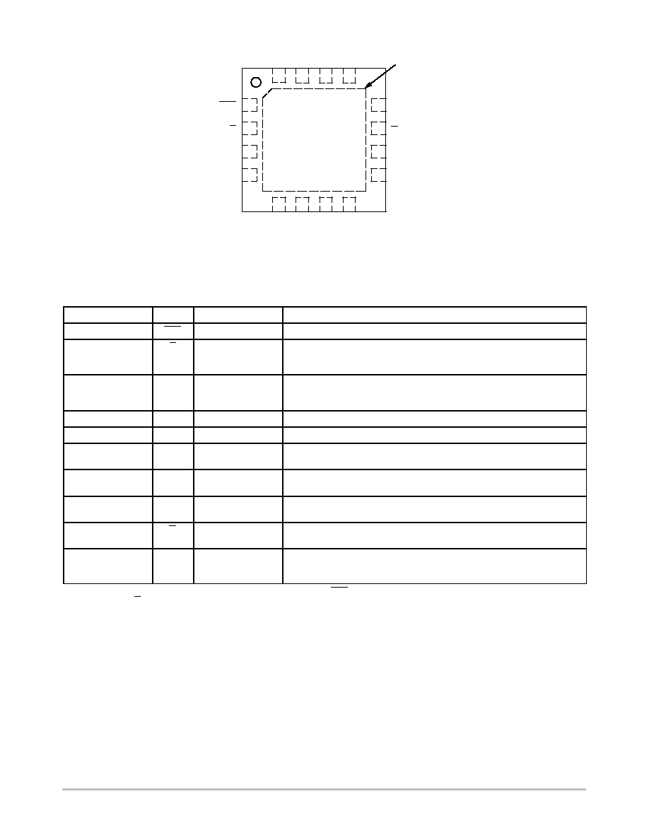
NB7L216
Exposed Pad (EP)
Figure 3. QFN-16 Pinout (Top View)
V
EE
V
EE
V
EE
Table 1. PIN DESCRIPTION
Pin
Name
I/O
Description
1
VTD
-
Internal 50
W
termination pin. See Table 7. Note 1
2
D
LVPECL, CML,
LVCMOS, LVDS,
LVTTL Input
Inverted differential input. Note 1.
3
D
LVPECL, CML,
LVCMOS, LVDS,
LVTTL Input
Noninverted differential input. Note 1.
4
VTD
-
Internal 50
W
termination pin. See Table 7. Note 1.
15
V
BB
-
Internally generated ECL reference voltage supply.
5, 6, 7, 8, 13, 14, 15
V
EE
-
Negative supply voltage. All V
EE
pins must be externally connected to power
supply to guarantee proper operation.
9, 12
V
CC
-
Positive supply voltage. All V
CC
pins must be externally connected to power
supply to guarantee proper operation
10
Q
RSECL Output
Noninverted differential output. Typically receiver terminated with 50
W
resistor
to V
TT
= V
CC
- 2.0 V.
11
Q
RSECL Output
Inverted differential output. Typically receiver terminated with 50
W
resistor to
V
TT
= V
CC
- 2.0 V.
-
EP
-
Exposed pad (EP). Thermally exposed pad on the package bottom must be
attached to a heat sinking conduit. It is recommended to connect the EP to the
lower potential, V
EE
.
1. In the differential configuration when the input termination pins (VTD, VTD) are connected to a common termination voltage and if no signal
is applied on D/D input then the device will be susceptible to self-oscillation.

NB7L216
http://onsemi.com
3
Table 2. ATTRIBUTES
Characteristics
Value
ESD Protection
Human Body Model
Machine Model
Charged Device Model
> 500 kV
> 50 V
> 4 kV
Moisture Sensitivity (Note 2)
QFN-16
Level 1
Flammability Rating
Oxygen Index: 28 to 34
UL 94 V-0 @ 0.125 in
Transistor Count
164
Meets or exceeds JEDEC Spec EIA/JESD78 IC Latchup Test.
2. For additional information, see Application Note AND8003/D.
Table 3. MAXIMUM RATINGS
(Note 3)
Symbol
Parameter
Condition 1
Condition 2
Rating
Unit
V
CC
Positive Power Supply
V
EE
= 0 V
3.6
V
V
EE
Negative Power Supply
V
CC
= 0 V
-3.6
V
V
I
Positive Input
Negative Input
V
EE
= 0 V
V
CC
= 0 V
V
I
= V
CC
V
I
= V
EE
3.6
-3.6
V
V
V
INPP
Differential Input Voltage
|D - D|
2.8
V
I
IN
Input Current Through R
T
(50
W
Resistor)
Static
Surge
45
80
mA
mA
I
OUT
Output Current
Continuous
Surge
25
50
mA
mA
I
BB
V
BB
Sink/Source
±
0.5
mA
T
A
Operating Temperature Range
-40 to +85
°
C
T
stg
Storage Temperature Range
-65 to +150
°
C
q
JA
Thermal Resistance (Junction-to-Ambient)
(Note 4)
0 lfpm
500 lfpm
QFN-16
QFN-16
42
35
°
C/W
°
C/W
q
JC
Thermal Resistance (Junction-to-Case)
1S2P (Note 4)
QFN-16
4
°
C/W
T
sol
Wave Solder
Pb
Pb-Free
<2 Sec @ 248
°
C
<2 Sec @ 260
°
C
265
265
°
C
Maximum ratings are those values beyond which device damage can occur. Maximum ratings applied to the device are individual stress limit
values (not normal operating conditions) and are not valid simultaneously. If these limits are exceeded, device functional operation is not implied,
damage may occur and reliability may be affected.
3. Maximum ratings applied to the device are individual stress limit values (not normal operating conditions) and are not valid simultaneously.
If stress limits are exceeded device functional operation is not implied, damage may occur and reliability may be affected.
4. JEDEC standard multilayer board - 1S2P (1 signal, 2 power) with 8 filled thermal vias under exposed pad.

NB7L216
http://onsemi.com
4
Table 4. DC CHARACTERISTICS, CLOCK INPUTS, CML OUTPUTS
V
CC
= 2.375 V to 3.465 V, V
EE
= 0 V
-40
5
C
25
5
C
85
5
C
Symbol
Characteristic
Min
Typ
Max
Min
Typ
Max
Min
Typ
Max
Unit
I
EE
Power Supply Current (VTD/VTD
open)
27
35
27
35
27
35
mA
V
OH
Output HIGH Voltage
(Note 5 and 6)
V
CC
-1040
V
CC
-980
V
CC
-940
V
CC
-1000
V
CC
-950
V
CC
-900
V
CC
950
V
CC
-900
V
CC
-850
mV
V
OL
Output LOW Voltage
(Note 5 and 6)
V
CC
-1520
V
CC
-1430
V
CC
-1320
V
CC
-1470
V
CC
-1370
V
CC
-1270
V
CC
1440
V
CC
-1340
V
CC
-1240
mV
DIFFERENTIAL INPUT DRIVEN SINGLE-ENDED (see Figures 14 and 16)
V
TH
Input Threshold Reference Voltage
Range (Note 7 and 8)
1100
V
CC
-10
1100
V
CC
-10
1100
V
CC
-10
mV
V
IH
Single-ended Input HIGH Voltage
(Note 8)
V
th
+10
V
CC
V
th
+ 10
V
CC
V
th
+10
V
CC
mV
V
IL
Single-ended Input LOW Voltage
(Note 8)
V
EE
V
th
-10
V
EE
V
th
-10
V
EE
V
th
-10
mV
DIFFERENTIAL INPUTS DRIVEN DIFFERENTIALLY (see Figures 15 and 17)
V
IHD
Differential Input HIGH Voltage
(Note 9)
1105
V
CC
1105
V
CC
1105
V
CC
mV
V
ILD
Differential Input LOW Voltage
(Note 9)
V
EE
V
CC
-10
V
EE
V
CC
-10
V
EE
V
CC
-10
mV
V
CMR
Input Common Mode Range
(Differential Configuration,
Note 9 and 10)
1100
V
CC
-5
1100
V
CC
5
1100
V
CC
5
mV
V
ID
Differential Input Voltage
(V
IHD
- V
ILD
)
10
2500
10
2500
10
2500
mV
V
IO
Input Offset Voltage (Note 11)
-5
0
+5
-5
0
+5
-5
0
+5
mV
V
BB
Internally Generated Reference
Voltage Supply
(Only 3 V 3.6 V Supply Load with
-100
m
A)
V
CC
-1425
V
CC
-1345
V
CC
-1265
V
CC
-1425
V
CC
-1345
V
CC
-1265
V
CC
-1425
V
CC
-1345
V
CC
-1265
mV
I
IH
Input HIGH Current
D/Db (VTD/VTD Open)
0
20
100
0
20
100
0
20
100
m
A
I
IL
Input LOW Current
D/Db (VTD/VTD Open)
-25
10
75
-25
10
75
-25
10
75
m
A
R
TIN
Internal Input Termination Resistor
45
50
55
45
50
55
45
50
55
W
R
T_Coef
Internal Input Termination Resistor
Temperature Coefficient
6.38
6.38
6.38
m
W/
°
C
NOTE: Device will meet the specifications after thermal equilibrium has been established when mounted in a test socket or printed circuit
board with maintained airflow greater than 500 lfpm. Electrical parameters are guaranteed only over the declared operating
temperature range. Functional operation of the device exceeding these conditions is not implied. Device specification limit values
are applied individually under normal operating conditions and not valid simultaneously.
5. Outputs evaluated with 50
W
resistors to V
TT
= V
CC
- 2.0 V for proper operation.
6. Input and output parameters vary 1:1 with V
CC
.
7. V
TH
is applied to the complementary input when operating in single-ended mode.
8. V
IH
, V
IL
and V
TH
parameters must be complied simultaneously.
9. V
IHD
, V
ILD
and V
CMR
parameters must be complied simultaneously.
10. V
CMR
min varies 1:1 with V
EE
, V
CMR
max varies 1:1 with V
CC
.
11. Typical standard deviation of input offset voltage is 1.76 mV.

NB7L216
http://onsemi.com
5
Table 5. AC CHARACTERISTICS
V
CC
= 2.375 V to 3.465 V, V
EE
= 0 V; (Note 12)
-40
°
C
25
°
C
85
°
C
Symbol
Characteristic
Min
Typ
Max
Min
Typ
Max
Min
Typ
Max
Unit
V
OUTPP
Output Voltage Amplitude (@ V
INPPmin
) f
in
7.0 GHz
(See Figure 4)
f
in
8.5 GHz
275
100
380
250
275
100
380
250
275
100
380
250
mV
f
DATA
Maximum Operating Data Rate
10
12
10
12
10
12
Gb/s
|S21|
Power Gain DC to 7 GHz
35
35
35
dB
|S11|
Input Return Loss @ 7 GHz
-10
-10
-10
dB
|S22|
Output Return Loss @ 7 GHz
-5
-5
-5
dB
|S12|
Reverse Isolation (Differential Configuration)
-25
-25
-25
dB
IIP3
Input Third Order Intercept
0
0
0
dBm
t
PLH
,
t
PHL
Propagation Delay to Output Differential @ 1 GHz
60
120
180
60
120
180
60
120
180
ps
t
SKEW
Duty Cycle Skew (Note 12)
Device to Device Skew (Note 17)
2
5
10
20
2
5
10
20
2
5
10
20
ps
t
JITTER
RMS Random Clock Jitter
f
in
v
8.5 GHz
(Note 15)
Peak-to-Peak Data Dependent Jitter (Note 16)
f
DATA
= 3.5 Gb/s
f
DATA
= 5.0 Gb/s
f
DATA
= 10 Gb/s
f
DATA
= 12 Gb/s
0.1
1
3
4
4
0.5
7
9
9
9
0.1
1
3
4
4
0.5
7
9
9
9
0.1
1
3
4
4
0.5
7
9
9
9
ps
V
INPP
Input Voltage Swing/Sensitivity
(Differential Configuration) (Note 14 and Figure 12)
20
2500
20
2500
20
2500
mV
t
r
t
f
Output Rise/Fall Times @ 0.5 GHz
Q, Q
(20% - 80%)
30
45
30
45
30
45
ps
NOTE: Device will meet the specifications after thermal equilibrium has been established when mounted in a test socket or printed circuit
board with maintained airflow greater than 500 lfpm. Electrical parameters are guaranteed only over the declared operating
temperature range. Functional operation of the device exceeding these conditions is not implied. Device specification limit values
are applied individually under normal operating conditions and not valid simultaneously.
12. Measured by forcing V
INPPmin
from a 50% duty cycle clock source. All loading with an external R
L
= 50
W
to V
TT
=V
CC
- 2.0 V. Input edge
rates 40 ps (20% - 80%).
13. Duty cycle skew is measured between differential outputs using the deviations of the sum of Tpw- and Tpw+ @ 1 GHz.
14. V
INPP
(MAX) cannot exceed V
CC
- V
EE
. Input voltage swing is a single-ended measurement operating in differential mode.
15. Additive RMS jitter with 50% duty cycle clock signal.
16. Additive peak-to-peak data dependent jitter with input NRZ data at PRBS 2
23
-1.
17. Device to device skew is measured between outputs under identical transition @ 1 GHz.
0
50
100
150
200
250
300
350
400
450
500
2
4
6
7
8
9
10
11
12
0
Figure 4. Output Voltage Amplitude (V
OUTPP
) versus
Input Clock Frequency (f
IN
) and Temperature
(V
INPP
= 400 mV, V
CC
= 3.3 V and V
EE
= 0 V)
25
°
C
-40
°
C
85
°
C
INPUT CLOCK FREQUENCY (GHz)
OUTPUT
VOL
T
AGE
AMPLITUDE (mV)
0
50
100
150
200
250
300
350
400
450
500
2
4
6
7
8
9
10
11
12
0
-40
°
C
25
°
C
85
°
C
INPUT CLOCK FREQUENCY (GHz)
OUTPUT
VOL
T
AGE
AMPLITUDE (mV)
Figure 5. Output Voltage Amplitude (V
OUTPP
) versus
Input Clock Frequency (f
IN
) and Temperature
(V
INPP
= 20 mV, V
CC
= 3.3 V and V
EE
= 0 V)

NB7L216
http://onsemi.com
6
TIME (66 ps/div)
Figure 6. Typical Output Waveform at 2.488 Gb/s with
PRBS 2
23
-1 (V
INPP
= 400 mV, Input Signal DDJ = 12 ps)
VOL
T
AGE (60 mV/div)
TIME (54 ps/div)
Figure 7. Typical Output Waveform at 3.5 Gb/s with
PRBS 2
23
-1 (V
INPP
= 400 mV, Input Signal DDJ = 12 ps)
VOL
T
AGE (60 mV/div)
VOL
T
AGE (60 mV/div)
TIME (37 ps/div)
Figure 8. Typical Output Waveform at 5 Gb/s with PRBS
2
23
-1 (V
INPP
= 400 mV, Input Signal DDJ = 12 ps)
TIME (21 ps/div)
Figure 9. Typical Output Waveform at 10 Gb/s with
PRBS 2
23
-1 (V
INPP
= 400 mV, Input Signal DDJ = 12 ps)
VOL
T
AGE (60 mV/div)
Device DDJ = 1 ps
Device DDJ =1 ps
Device DDJ =2 ps
Device DDJ = 3 ps
FREQUENCY (GHz)
GAIN (dB)
0
5
10
15
20
25
30
35
40
Figure 10. Small Signal Gain S21 Magnitude*
-50
-40
-30
-20
-10
0
GAIN (dB)
FREQUENCY (GHz)
Figure 11. Input and Output Reflection S11
and S22 Magnitude*
0
S11
S22
2
4
6
8
10
12
14
16
0
2
4
6
8
10
12
14
16
*T
A
= +25
°
C, V
CC
= 3.3 V, V
EE
=0 V, P
IN
= -44 dBm,Z
S
= Z
L
= 50
W
, input and output matching network is not included.

NB7L216
http://onsemi.com
7
Table 6. TYPICAL DEVICE S-PARAMETERS
Frequency
S11
S21
S12
S22
Frequency
(Hz)
dbS11
|S11|
í
S11
dbS21
|S21|
í
S21
dbS12
|S12|
í
S12
dbS22
|S22|
í
S22
4.97E+08
-45.2
0.005
-88.5
37.2
72.799
-33.2
-72.3
0.001
-139.1
-2.5
0.749
157.4
1.02E+09
-30.4
0.030
-134.7
37.3
73.145
-68.4
-45.8
0.005
129.8
-2.9
0.714
154.3
1.51E+09
-36.2
0.015
-146.5
37.1
71.433
-105.4
-43.3
0.007
98.5
-2.9
0.717
132.8
2.00E+09
-27.4
0.042
25.7
37.4
74.061
-139.0
-37.1
0.014
91.8
-3.5
0.666
107.1
2.52E+09
-12.3
0.244
-27.7
36.2
64.810
-179.5
-29.9
0.032
54.4
-4.4
0.599
92.1
3.01E+09
-10.6
0.295
-83.8
36.9
70.102
144.5
-26.1
0.050
9.4
-6.3
0.485
77.3
3.50E+09
-19.0
0.112
-22.1
35.4
58.933
99.9
-28.3
0.038
25.9
-5.0
0.566
67.9
4.02E+09
-10.6
0.294
-120.3
35.6
60.437
73.8
-24.8
0.058
-32.6
-7.6
0.417
54.2
4.51E+09
-10.7
0.291
167.4
36.0
62.843
41.1
-22.5
0.075
-68.3
-13.9
0.201
70.2
4.99E+09
-9.0
0.354
87.1
35.1
56.576
14.2
-25.2
0.055
-107.2
-8.7
0.367
81.2
5.48E+09
-10.6
0.294
62.7
36.4
65.812
-16.1
-24.3
0.061
-121.4
-8.0
0.398
50.4
6.01E+09
-9.3
0.341
108.2
35.8
61.327
-72.8
-24.5
0.060
-125.7
-8.0
0.397
-0.9
6.49E+09
-9.4
0.340
59.4
36.2
64.212
-119.4
-21.9
0.080
-152.4
-12.5
0.237
-27.2
6.98E+09
-17.5
0.133
25.5
34.3
52.039
-141.5
-22.7
0.073
177.5
-7.4
0.428
-32.2
7.51E+09
-25.6
0.053
107.9
33.2
45.861
164.6
-24.4
0.060
165.7
-7.0
0.445
-37.9
7.99E+09
-13.7
0.206
146.5
25.2
18.093
133.6
-21.5
0.084
152.8
-7.6
0.416
-54.7
8.52E+09
-6.7
0.462
117.9
22.6
13.434
116.2
-19.4
0.107
120.7
-12.1
0.249
-73.7
9.00E+09
-5.2
0.552
106.2
19.4
9.336
102.0
-19.0
0.112
109.9
-12.2
0.246
-62.5
9.49E+09
-3.7
0.652
71.1
19.0
8.937
61.1
-19.4
0.107
62.0
-11.5
0.267
-100.2
1.00E+10
-9.7
0.326
46.2
18.7
8.595
18.6
-24.0
0.063
50.6
-10.4
0.301
-117.0
1.05E+10
-11.0
0.283
35.8
14.5
5.298
-13.3
-25.9
0.051
12.9
-10.8
0.288
-172.0
1.10E+10
-8.3
0.384
7.2
12.9
4.408
-9.6
-29.4
0.034
21.1
-13.4
0.213
74.0
1.15E+10
-5.9
0.506
-0.4
12.7
4.339
-33.7
-21.4
0.085
36.3
-21.4
0.085
-148.6
1.20E+10
-9.0
0.356
-23.8
12.9
4.395
-63.4
-19.4
0.107
-9.5
-13.4
0.214
159.5
1.25E+10
-15.6
0.166
-46.9
10.5
3.360
-97.8
-21.0
0.089
-39.0
-12.4
0.239
169.2
1.30E+10
-15.1
0.175
-83.0
9.9
3.121
-119.7
-24.0
0.063
-39.9
-11.3
0.272
171.6
1.35E+10
-12.0
0.250
-96.5
8.7
2.728
-148.9
-22.0
0.079
-39.1
-14.9
0.181
177.8
1.40E+10
-11.5
0.265
-105.9
7.3
2.314
-167.1
-18.6
0.118
-74.2
-18.4
0.120
140.3
1.45E+10
-17.0
0.140
-97.8
5.4
1.856
167.6
-20.1
0.099
-107.0
-15.7
0.163
98.2
1.50E+10
-23.4
0.068
-108.9
4.6
1.695
145.0
-20.2
0.098
-128.1
-11.2
0.274
96.1
NOTE:
T
A
= +25
°
C, V
CC
=3.3V, V
EE
= 0 V, P
IN
= -44 dBm, Z
S
= Z
L
= 50
W
, input and output matching network is not included.

NB7L216
http://onsemi.com
8
Figure 12. AC Reference Measurement
D
D
Q
Q
t
PHL
t
PLH
V
INPP
= V
IH
(D) - V
IL
(D)
V
OUTPP
= V
OH
(Q) - V
OL
(Q)
Figure 13. Typical Termination for Output Driver and Device Evaluation
(See Application Note AND8020/D - Termination of ECL Logic Devices.)
Driver
Device
Receiver
Device
Q
D
Q
D
Z
o
= 50
W
Z
o
= 50
W
50
W
50
W
V
TT
V
TT
= V
CC
- 2.0 V
Figure 14. Differential Input Driven
Single-Ended
Figure 15. Differential Inputs Driven
Differentially
Figure 16. V
th
Diagram
Figure 17. V
CMR
Diagram
D
V
CC
GND
V
IH
V
IHmin
V
IHmax
V
thmax
V
th
V
th
V
thmin
V
CMmax
V
CMmax
D
V
CMR
V
CC
GND
D
D
V
th
V
th
D
D
V
ILmax
V
IL
V
ILmin
D
V
ILDmax
V
IHDmax
V
ID
= V
IHD
- V
ILD
V
ILDtyp
V
IHDtyp
V
ILDmin
V
IHDmin
NOTE:
V
EE
v
V
IN
v
V
CC
; V
IH
> V
IL

NB7L216
http://onsemi.com
9
APPLICATION INFORMATION
All NB7L216 inputs can accept PECL, CML, LVTTL, LVCMOS and LVDS signal levels. The limitations for differential
input signal (LVDS, PECL, or CML) are minimum input swing of 75 mV and the maximum input swing of 2500 mV. Within
these conditions, the input voltage can range from V
CC
to 1.2 V. Examples interfaces are illustrated below in a 50
W
environment (Z = 50
W). For output termination and interface, refer to application note AND8020/D.
Table 7. INTERFACING OPTIONS
Interfacing Options
Connections
CML
Connect VTD and VTD to V
CC
(See Figure 18)
LVDS
Connect VTD and VTD Together (See Figure 20)
AC-COUPLED
Bias VTD and VTD Inputs within Common Mode Range (V
CMR
) (See Figure 19)
RSECL, PECL, NECL
Standard ECL Termination Techniques (See Figure 13)
LVTTL, LVCMOS
An External Voltage (V
THR
) should be Applied to the Unused Complementary Differential Input. Nominal
V
THR
is 1.5 V for LVTTL and V
CC
/ 2 for LVCMOS Inputs. This Voltage must be within the
V
THR
Specification. (See Figure 21)
50
W
V
CC
D
D
50
W
NB7L216
V
CC
VTD
V
EE
V
CC
Q
50
W
50
W
CML
Driver
V
EE
Figure 18. CML to NB7L216 Interface
Q
Z = 50
W
Figure 19. PECL to NB7L216 Interface
50
W
V
CC
V
CC
PECL
Driver
D
D
50
W
NB7L216
V
EE
V
Bias
*
VTD
V
EE
R
T
R
T
V
EE
V
CC
R
T
5.0 V 290
W
3.3 V 150
W
2.5 V
80
W
Recommended R
T
Values
VTD
V
CC
VTD
V
Bias
*
Z = 50
W
Z = 50
W
Z = 50
W
C
C
*V
Bias
must be within common mode range limits (V
CMR
)

NB7L216
http://onsemi.com
10
50
W
V
CC
V
CC
LVDS
Driver
D
D
50
W
NB7L216
V
EE
VTD
V
EE
VTD
Figure 20. LVDS to NB7L216 Interface
Figure 21. LVCMOS/LVTTL to NB7L216 Interface
50
W
V
CC
V
CC
LVTTL/
LVCMOS
Driver
D
D
50
W
NB7L216
V
EE
VTD
V
CC
V
REF
LVCMOS V
CC
- V
EE
2
LVTTL
1.5 V
Recommended V
REF
Values
VTD
V
REF
No Connect*
No Connect
*or 60 pF to GND
Z = 50
W
Z = 50
W
Z = 50
W

NB7L216
http://onsemi.com
11
ORDERING INFORMATION
Device
Package
Shipping
NB7L216MN
QFN-16
123 Units / Rail
NB7L216MNG
QFN-16
(Pb-Free)
123 Units / Rail
NB7L216MNR2
QFN-16
3000 / Tape & Reel
NB7L216MNR2G
QFN-16
(Pb-Free)
3000 / Tape & Reel
For information on tape and reel specifications, including part orientation and tape sizes, please refer to our Tape and Reel Packaging
Specifications Brochure, BRD8011/D.

NB7L216
http://onsemi.com
12
PACKAGE DIMENSIONS
16 PIN QFN
CASE 485G-01
ISSUE B
16X
SEATING
PLANE
L
D
E
0.15 C
A
A1
e
D2
E2
b
1
4
5
8
12
9
16
13
NOTES:
1. DIMENSIONING AND TOLERANCING PER
ASME Y14.5M, 1994.
2. CONTROLLING DIMENSION: MILLIMETERS.
3. DIMENSION b APPLIES TO PLATED
TERMINAL AND IS MEASURED BETWEEN
0.25 AND 0.30 MM FROM TERMINAL.
4. COPLANARITY APPLIES TO THE EXPOSED
PAD AS WELL AS THE TERMINALS.
5. L
max
CONDITION CAN NOT VIOLATE 0.2 MM
MINIMUM SPACING BETWEEN LEAD TIP
AND FLAG
ÇÇÇ
ÇÇÇ
ÇÇÇ
B
A
0.15 C
TOP VIEW
SIDE VIEW
BOTTOM VIEW
PIN 1
LOCATION
0.10 C
0.08 C
(A3)
C
16 X
e
16X
NOTE 5
0.10 C
0.05 C
A B
NOTE 3
K
16X
DIM
MIN
MAX
MILLIMETERS
A
0.80
1.00
A1
0.00
0.05
A3
0.20 REF
b
0.18
0.30
D
3.00 BSC
D2
1.65
1.85
E
3.00 BSC
E2
1.65
1.85
e
0.50 BSC
K
0.20
---
L
0.30
0.50
EXPOSED PAD
mm
inches
SCALE 10:1
0.50
0.02
0.575
0.022
1.50
0.059
3.25
0.128
0.30
0.012
3.25
0.128
0.30
0.012
EXPOSED PAD
*For additional information on our Pb-Free strategy and soldering
details, please download the ON Semiconductor Soldering and
Mounting Techniques Reference Manual, SOLDERRM/D.
SOLDERING FOOTPRINT*
ON Semiconductor and are registered trademarks of Semiconductor Components Industries, LLC (SCILLC). SCILLC reserves the right to make changes without further notice
to any products herein. SCILLC makes no warranty, representation or guarantee regarding the suitability of its products for any particular purpose, nor does SCILLC assume any liability
arising out of the application or use of any product or circuit, and specifically disclaims any and all liability, including without limitation special, consequential or incidental damages.
"Typical" parameters which may be provided in SCILLC data sheets and/or specifications can and do vary in different applications and actual performance may vary over time. All
operating parameters, including "Typicals" must be validated for each customer application by customer's technical experts. SCILLC does not convey any license under its patent rights
nor the rights of others. SCILLC products are not designed, intended, or authorized for use as components in systems intended for surgical implant into the body, or other applications
intended to support or sustain life, or for any other application in which the failure of the SCILLC product could create a situation where personal injury or death may occur. Should
Buyer purchase or use SCILLC products for any such unintended or unauthorized application, Buyer shall indemnify and hold SCILLC and its officers, employees, subsidiaries, affiliates,
and distributors harmless against all claims, costs, damages, and expenses, and reasonable attorney fees arising out of, directly or indirectly, any claim of personal injury or death
associated with such unintended or unauthorized use, even if such claim alleges that SCILLC was negligent regarding the design or manufacture of the part. SCILLC is an Equal
Opportunity/Affirmative Action Employer. This literature is subject to all applicable copyright laws and is not for resale in any manner.
PUBLICATION ORDERING INFORMATION
N. American Technical Support: 800-282-9855 Toll Free
USA/Canada
Japan: ON Semiconductor, Japan Customer Focus Center
2-9-1 Kamimeguro, Meguro-ku, Tokyo, Japan 153-0051
Phone: 81-3-5773-3850
NB7L216/D
LITERATURE FULFILLMENT:
Literature Distribution Center for ON Semiconductor
P.O. Box 61312, Phoenix, Arizona 85082-1312 USA
Phone: 480-829-7710 or 800-344-3860 Toll Free USA/Canada
Fax: 480-829-7709 or 800-344-3867 Toll Free USA/Canada
Email: orderlit@onsemi.com
ON Semiconductor Website: http://onsemi.com