
©
Semiconductor Components Industries, LLC, 2003
April, 2003 - Rev. 4
1
Publication Order Number:
NB100LVEP17/D
NB100LVEP17
2.5V / 3.3V / 5V ECL Quad
Differential Driver/Receiver
The NB100LVEP17 is a 4-bit differential line receiver. The design
incorporates two stages of gain, internal to the device, making it an
excellent choice for use in high bandwidth amplifier applications.
The V
BB
pin, an internally generated voltage supply, is available to
this device only. For single-ended input conditions, the unused
differential input is connected to V
BB
as a switching reference voltage.
V
BB
may also rebias AC coupled inputs. When used, decouple V
BB
and V
CC
via a 0.01
mF capacitor and limit current sourcing or sinking
to 0.5 mA. When not used, V
BB
should be left open.
Inputs of unused gates can be left open and will not affect the
operation of the rest of the device.
∑
Maximum Input Clock Frequency > 2.5 GHz Typical
∑
Maximum Input Data Rate > 2.5 Gb/s Typical
∑
250 ps Typical Propagation Delay
∑
Low Profile QFN Package
∑
PECL Mode Operating Range: V
CC
= 2.375 V to 5.5 V
with V
EE
= 0 V
∑
NECL Mode Operating Range: V
CC
= 0 V
with V
EE
= -2.375 V to -5.5 V
∑
Q Output Will Default LOW with Inputs Open or at V
EE
∑
V
BB
Output
TSSOP-20
DT SUFFIX
CASE 948E
MARKING
DIAGRAMS*
*For additional information, see Application Note
AND8002/D
N100
LP17
ALYW
20
1
1
20
http://onsemi.com
A = Assembly Location
L
= Wafer Lot
Y = Year
W = Work Week
N100
LP17
ALYW
1
24
24 PIN QFN
MN SUFFIX
CASE 485L
24
1
Device
Package
Shipping
ORDERING INFORMATION
NB100LVEP17DT
TSSOP-20
75 Units/Rail
NB100LVEP17DTR2
2500/Tape & Reel
TSSOP-20
NB100LVEP17MN
QFN-24
92 Units/Rail
NB100LVEP17MNR2
3000/Tape & Reel
QFN-24

NB100LVEP17
http://onsemi.com
2
D1
D1
D2
Q0
Q1
Q1
V
EE
D0
Q0
D2
D0
D3
D3
V
CC
Figure 1. Logic Diagram
Q2
Q3
Q3
Q2
V
BB
R1
R1
R1
R1
R1
R1
R1
R1
R2
R2
R2
R2
PIN DESCRIPTION
Pin
Default
¡¡¡¡¡
¡¡¡¡¡
TSSOP
¡¡¡¡
¡¡¡¡
QFN
Name
I/O
Default
State
Description
1,20
13,18,21,
22,23
V
CC
-
-
Positive Supply Voltage. All V
CC
Pins Must be Externally Connected
to Power Supply to Guarantee Proper Operation.
11
10
V
EE
-
-
Negative Supply Voltage. All V
EE
Pins Must be Externally Con-
nected to Power Supply to Guarantee Proper Operation.
10
9
V
BB
-
-
ECL Reference Voltage Output.
2,4,6,8
1,3,5,7
D[0:3]
ECL Input
Low
Noninverted Differential Inputs [0:3]. Internal 75 k
W
to V
EE
.
3,5,7,9
2,4,6,8
D[0:3]
ECL Input
High
Inverted Differential Inputs [0:3]. Internal 75 k
W
to V
EE
and 37 k
W
to
V
CC
.
19,17,15,13
12,15,17,2
0
Q[0:3]
ECL Output
-
Noninverted Differential Outputs [0:3]. Typically Terminated with
50
W
to V
TT
= V
CC
- 2 V.
18,16,14,12
11,14,16,1
9
Q[0:3]
ECL Output
-
Inverted Differential Outputs [0:3]. Typically Terminated with 50
W
to
V
TT
= V
CC
- 2 V.
N/A
24
NC
-
-
No Connect. The NC Pin is Electrically Connected to the Die and
"MUST BE" Left Open.
N/A
-
EP
-
Exposed Pad. (Note 1)
1. All V
CC
and V
EE
pins must be externally connected to Power Supply to guarantee proper operation. The thermally conductive expose pad
on the package bottom (see case drawing) must be attached to a heat-sinking conduit.

NB100LVEP17
http://onsemi.com
3
D1
D1
D2
D3
17
18
16
15
14
13
12
4
3
5
6
7
8
9
Q0
11
10
Q1
Q1
Q2
Q2
Q3
Q3 V
EE
D0
19
20
2
1
V
CC
Q0
D0
D2
V
CC
D3 V
BB
Figure 2. TSSOP-20 Lead Pinout (Top View)
D1
D1
D2
D3
Q0
Q1
Q1
Q2
Q2
Q3
Q3
V
EE
D0
V
CC
Q0
D0
D2
V
CC
D3
V
BB
V
CC
V
CC
V
CC
NC
Figure 3. QFN-24 Lead Pinout (Top View)
NB100LVEP17
NB100LVEP17
18
12
4
3
5
6
7
8
9
11
10
2
1
17
16
15
14
13
19
24
23
22
20
21
Exposed Pad
(EP)
Table 1. ATTRIBUTES
Characteristics
Value
Internal Input Pulldown Resistor
(R1)
75 k
W
Internal Input Pullup Resistor
(R2)
37 k
W
ESD Protection
Human Body Model
Machine Model
Charged Device Model
> 2 kV
> 150 V
> 2 kV
Moisture Sensitivity, Indefinite Time Out of Drypack (Note 1)
Level 1
Flammability Rating
Oxygen Index: 28 to 34
UL 94 V-0 @ 0.125 in
Transistor Count
274 Devices
Meets or exceeds JEDEC Spec EIA/JESD78 IC Latchup Test
1. For additional information, see Application Note AND8003/D.

NB100LVEP17
http://onsemi.com
4
Table 2. MAXIMUM RATINGS
(Note 2)
Symbol
Parameter
Condition 1
Condition 2
Rating
Units
V
CC
Positive Mode Power Supply
V
EE
= 0 V
6
V
V
EE
Negative Mode Power Supply
V
CC
= 0 V
-6
V
V
I
Positive Mode Input Voltage
Negative Mode Input Voltage
V
EE
= 0 V
V
CC
= 0 V
V
I
v
V
CC
V
I
w
V
EE
6
-6
V
V
I
out
Output Current
Continuous
Surge
50
100
mA
mA
I
BB
V
BB
Sink/Source
$
0.5
mA
TA
Operating Temperature Range
-40 to +85
∞
C
T
stg
Storage Temperature Range
-65 to +150
∞
C
q
JA
Thermal Resistance (Junction-to-Ambient)
JEDEC 51-3 (1S - Single Layer Test Board)
0 LFPM
500 LFPM
20 TSSOP
20 TSSOP
140
50
∞
C/W
∞
C/W
q
JA
Thermal Resistance (Junction-to-Ambient)
JEDEC 51-6 (2S2P Multilayer Test Board) with Filled Thermal
Vias
0 LFPM
500 LFPM
24 QFN
24 QFN
37
32
∞
C/W
∞
C/W
q
JC
Thermal Resistance (Junction-to-Case)
Standard Board
20 TSSOP
24 QFN
23 to 41
11
∞
C/W
∞
C/W
T
sol
Wave Solder
<2 to 3 sec @ 248
∞
C
265
∞
C
2. Maximum Ratings are those values beyond which device damage may occur.
Table 3. DC CHARACTERISTICS, PECL
V
CC
= 2.5 V; V
EE
= 0 V (Note 3)
-40
∞
C
25
∞
C
85
∞
C
Symbol
Characteristic
Min
Typ
Max
Min
Typ
Max
Min
Typ
Max
Unit
I
EE
Negative Power Supply Current
30
40
50
30
40
50
30
40
55
mA
V
OH
Output HIGH Voltage (Note 4)
1355
1480
1605
1355
1480
1605
1355
1480
1605
mV
V
OL
Output LOW Voltage (Note 4)
555
775
900
555
775
900
555
775
900
mV
V
IH
Input HIGH Voltage (Single-Ended) (Note 5)
1335
1620
1335
1620
1275
1620
mV
V
IL
Input LOW Voltage (Single-Ended) (Note 5)
555
875
555
875
555
875
mV
V
IHCMR
Input HIGH Voltage Common Mode Range
(Differential Configuration) (Note 6)
1.2
2.5
1.2
2.5
1.2
2.5
V
I
IH
Input HIGH Current (@ V
IH
)
150
150
150
m
A
I
IL
Input LOW Current (@ V
IL
)
D
D
0.5
-150
0.5
-150
0.5
-150
m
A
NOTE:
100LVEP circuits are designed to meet the DC specifications shown in the above table, after thermal equilibrium has been established.
The circuit is in a test socket or mounted on a printed circuit board and transverse air flow greater than 500 lfpm is maintained.
3. Input and output parameters vary 1:1 with V
CC
. V
EE
can vary + 0.125 V to -1.3 V.
4. All loading with 50
W
to V
EE
= V
CC
- 2.0 V.
5. Do not use V
BB
at VCC < 3.0 V.
6. V
IHCMR
min varies 1:1 with V
EE
, V
IHCMR
max varies 1:1 with V
CC
. The V
IHCMR
range is referenced to the most positive side of the differential
input signal.
NB100LVEP17
http://onsemi.com
5
Table 4. DC CHARACTERISTICS, PECL
V
CC
= 3.3 V; V
EE
= 0 V (Note 7)
-40
∞
C
25
∞
C
85
∞
C
Symbol
Characteristic
Min
Typ
Max
Min
Typ
Max
Min
Typ
Max
Unit
I
EE
Negative Power Supply Current
30
40
50
30
40
50
30
40
55
mA
V
OH
Output HIGH Voltage (Note 8)
2155
2280
2405
2155
2280
2405
2155
2280
2405
mV
V
OL
Output LOW Voltage (Note 8)
1355
1575
1700
1355
1575
1700
1355
1575
1700
mV
V
IH
Input HIGH Voltage (Single-Ended)
2135
2420
2135
2420
2135
2420
mV
V
IL
Input LOW Voltage (Single-Ended)
1355
1675
1355
1675
1355
1675
mV
V
BB
ECL Output Reference Voltage (Note 9)
1775
1875
1975
1775
1875
1975
1775
1875
1975
mV
V
IHCMR
Input HIGH Voltage Common Mode Range
(Differential Configuration) (Note 10)
1.2
3.3
1.2
3.3
1.2
3.3
V
I
IH
Input HIGH Current (@ V
IH
)
150
150
150
m
A
I
IL
Input LOW Current (@ V
IL
)
D
D
0.5
-150
0.5
-150
0.5
-150
m
A
NOTE:
100LVEP circuits are designed to meet the DC specifications shown in the above table, after thermal equilibrium has been established.
The circuit is in a test socket or mounted on a printed circuit board and transverse air flow greater than 500 lfpm is maintained.
7. Input and output parameters vary 1:1 with V
CC
. V
EE
can vary + 0.925 V to -0.5 V.
8. All loading with 50
W
to V
CC
- 2.0 V.
9. Single ended input operation is limited V
CC
3.0 V in PECL mode.
10. V
IHCMR
min varies 1:1 with V
EE
, V
IHCMR
max varies 1:1 with V
CC
. The V
IHCMR
range is referenced to the most positive side of the differential
input signal.
Table 5. DC CHARACTERISTICS, PECL
V
CC
= 5.0 V, V
EE
= 0 V (Note 11)
-40
∞
C
25
∞
C
85
∞
C
Symbol
Characteristic
Min
Typ
Max
Min
Typ
Max
Min
Typ
Max
Unit
I
EE
Negative Power Supply Current
30
40
50
30
40
55
30
40
55
mA
V
OH
Output HIGH Voltage (Note 12)
3855
3980
4105
3855
3980
4105
3855
3980
4105
mV
V
OL
Output LOW Voltage (Note 12)
3055
3275
3400
3055
3275
3400
3055
3275
3400
mV
V
IH
Input HIGH Voltage
3775
4120
3775
4120
3775
4120
mV
V
IL
Input LOW Voltage
3055
3375
3055
3375
3055
3375
mV
V
BB
ECL Output Voltage Reference
3475
3575
3675
3475
3575
3675
3475
3575
3675
mV
V
IHCMR
Input HIGH Voltage Common Mode Range
(Differential Configuration) (Note 13)
1.2
5.0
1.2
5.0
1.2
5.0
V
I
IH
Input HIGH Current (@ V
IH
)
150
150
150
m
A
I
IL
Input LOW Current (@ V
IL
)
D
D
0.5
-150
0.5
-150
0.5
-150
m
A
NOTE: 100LVEP circuits are designed to meet the DC specifications shown in the above table after thermal equilibrium has been established.
The circuit is in a test socket or mounted on a printed circuit board and transverse airflow greater than 500 lfpm is maintained.
11. Input and output parameters vary 1:1 with V
CC
. V
EE
can vary +2.0 V to -0.5 V.
12. All loading with 50 ohms to V
CC
-2.0 V.
13. V
IHCMR
min varies 1:1 with V
EE
, V
IHCMR
max varies 1:1 with V
CC
. The V
IHCMR
range is referenced to the most positive side of the differential
input signal.

NB100LVEP17
http://onsemi.com
6
Table 6. DC CHARACTERISTICS, NECL
V
CC
= 0 V, V
EE
= -2.375 V to -3.8 V (Note 14)
-40
∞
C
25
∞
C
85
∞
C
Symbol
Characteristic
Min
Typ
Max
Min
Typ
Max
Min
Typ
Max
Unit
I
EE
Negative Power Supply Current
30
40
50
30
40
50
30
40
55
mA
V
OH
Output HIGH Voltage (Note 15)
-1 145
-1020
-895
-1 145
-1020
-895
-1 145
-1020
-895
mV
V
OL
Output LOW Voltage (Note 15)
-1945
-1725
-1600
-1945
-1725
-1600
-1945
-1725
-1600
mV
V
IH
Input HIGH Voltage (Single-Ended)
-1 165
-880
-1 165
-880
-1 165
-880
mV
V
IL
Input LOW Voltage (Single-Ended)
-1945
-1600
-1945
-1600
-1945
-1600
mV
V
BB
ECL Output Reference Voltage
(Note 16)
-1525
-1425
-1325
-1525
-1425
-1325
-1525
-1425
-1325
mV
V
IHCMR
Input HIGH Voltage Common Mode
Range (Differential Configuration)
(Note 17)
V
EE
+ 1.2
0.0
V
EE
+ 1.2
0.0
V
EE
+ 1.2
0.0
V
I
IH
Input HIGH Current (@ V
IH
)
150
150
150
m
A
I
IL
Input LOW Current (@ V
IL
)
D
D
0.5
-150
0.5
-150
0.5
-150
m
A
NOTE:
100LVEP circuits are designed to meet the DC specifications shown in the above table, after thermal equilibrium has been established.
The circuit is in a test socket or mounted on a printed circuit board and transverse air flow greater than 500 lfpm is maintained.
14. Input and output parameters vary 1:1 with V
CC
.
15. All loading with 50
W
to V
CC
- 2.0 V.
16. Single ended input operation is limited V
EE
-3.0V in NECL mode.
17. V
IHCMR
min varies 1:1 with V
EE
, V
IHCMR
max varies 1:1 with V
CC
. The V
IHCMR
range is referenced to the most positive side of the differential
input signal.
Table 7. DC CHARACTERISTICS, NECL
V
CC
= 0 V, V
EE
= -3.8 V to -5.5 V (Note 18)
-40
∞
C
25
∞
C
85
∞
C
Symbol
Characteristic
Min
Typ
Max
Min
Typ
Max
Min
Typ
Max
Unit
I
EE
Negative Power Supply Current
30
40
50
30
40
55
30
40
55
mA
V
OH
Output HIGH Voltage (Note 19)
-1 145
-1020
-895
-1 145
-1020
-895
-1 145
-1020
-895
mV
V
OL
Output LOW Voltage (Note 19)
-1945
-1725
-1600
-1945
-1725
-1600
-1945
-1725
-1600
mV
V
IH
Input HIGH Voltage
-1 165
-880
-1 165
-880
-1 165
-880
mV
V
IL
Input LOW Voltage
-1945
-1625
-1945
-1625
-1945
-1625
mV
V
BB
ECL Output Reference Voltage
(Note 20)
-1525
-1425
-1325
-1525
-1425
-1325
-1525
-1425
-1325
mV
V
IHCMR
Input HIGH Voltage Common Mode
Range (Differential Configuration)
(Note 21)
V
EE
+1.2
0.0
V
EE
+1.2
0.0
V
EE
+1.2
0.0
V
I
IH
Input HIGH Current (@ V
IH
)
150
150
150
m
A
I
IL
Input LOW Current (@ V
IL
)
D
D
0.5
-150
0.5
-150
0.5
-150
m
A
NOTE: 100LVEP circuits are designed to meet the DC specifications shown in the above table after thermal equilibrium has been established.
The circuit is in a test socket or mounted on a printed circuit board and transverse airflow greater than 500 lfpm is maintained.
18. Input and output parameters vary 1:1 with V
CC
.
19. All loading with 50
W
to V
CC
-2.0 V.
20. Single-Ended input operation is limited to V
EE
from -3.0 V to -5.5 V in NECL mode.
21. V
IHCMR
min varies 1:1 with V
EE
, V
IHCMR
max varies 1:1 with V
CC
. The V
IHCMR
range is referenced to the most positive side of the differential
input signal.

NB100LVEP17
http://onsemi.com
7
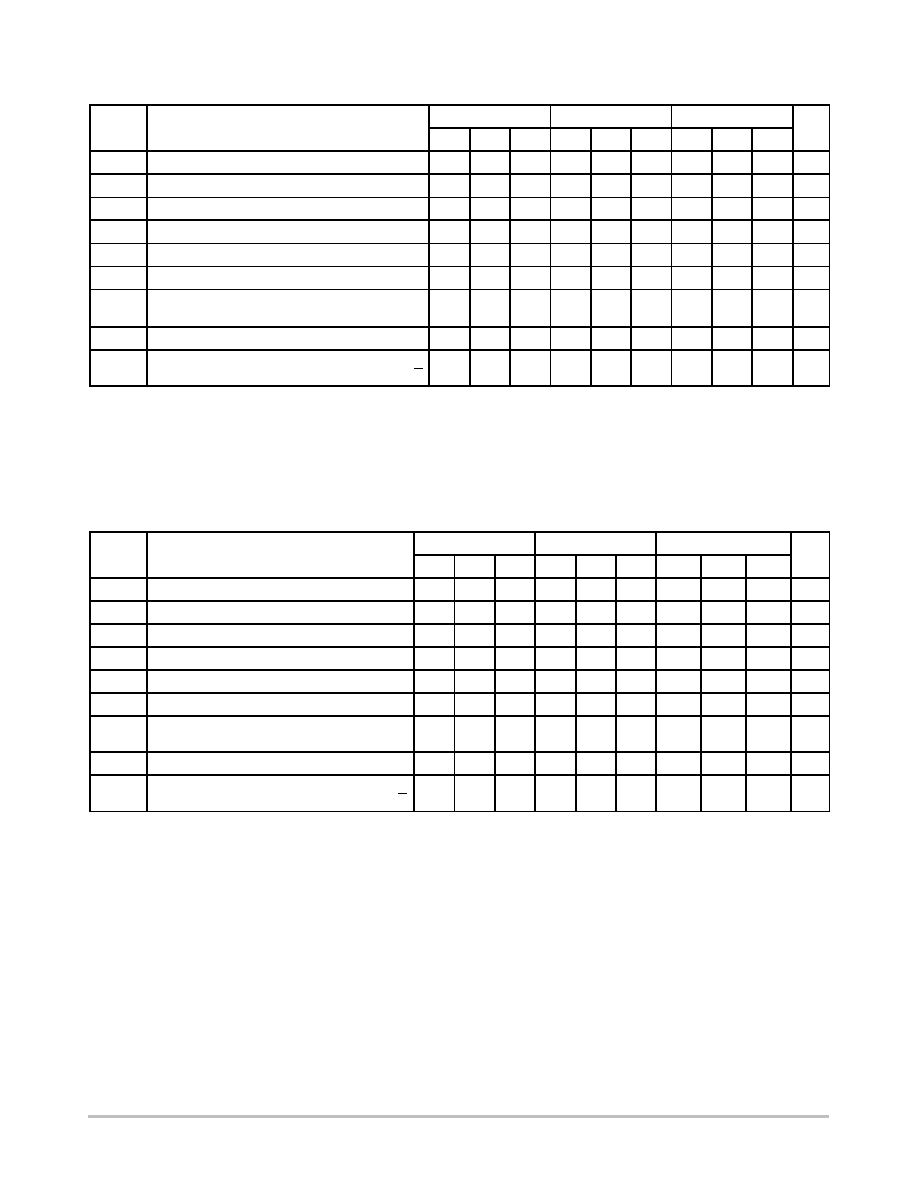
Table 8. AC CHARACTERISTICS
V
CC
= 0 V; V
EE
= -2.375 V to -3.8 V or V
CC
= 2.375 V to 3.8 V; V
EE
= 0 V (Note 22)
-40
∞
C
25
∞
C
85
∞
C
Symbol
Characteristic
Min
Typ
Max
Min
Typ
Max
Min
Typ
Max
Unit
V
OUTPP
Output Voltage Amplitude
f
in
< 1 GHz
(See Figures 4, 5)
f
in
= 2 GHz
f
in
= 2.5 GHz
600
400
300
700
500
400
600
325
250
700
500
400
550
300
200
700
500
400
mV
t
PLH
,
t
PHL
Propagation Delay to Output Differential
D to Q, Q
200
250
325
200
250
325
225
300
350
ps
t
Skew
Pulse Skew (Note 23)
Within Device Skew (Note 25)
Device-to-Device Skew (Note 25)
5
5
25
25
25
100
5
5
25
25
25
100
5
5
25
25
25
100
ps
t
JITTER
RMS Random Clock Jitter (Note 26)
f
in
= 2.5 GHz
Peak-to Peak Data Dependent Jitter
f
in
= 1.5 Gb/s
(Note 27)
f
in
= 2.5 Gb/s
0.5
5
5
1
15
15
0.5
5
5
1
15
15
0.5
5
5
1
15
15
ps
V
INPP
Input Voltage Swing (Differential Configuration)
(Note 28)
150
800
1200
150
800
1200
150
800
1200
mV
t
r
t
f
Output Rise/Fall Times @ 50 MHz
Q, Q
(20% - 80%)
125
175
225
140
190
240
150
200
250
ps
22. Measured using a 750 mV source, 50% duty cycle clock source. All loading with 50
W
to V
CC
-2.0 V. Input edge rates 150 ps (20% - 80%).
23. Pulse Skew = |t
PLH
- t
PHL
|
24. Worst case difference between Q0 and Q1 outputs.
25. Skew is measured between outputs under identical transitions.
26. Additive RMS jitter with 50% Duty Cycle Clock Signal at 2.5 GHz.
27. Peak-to-Peak jitter with input NRZ data at PRBS 2
31
-1 at 2.5 Gb/s with all inputs active.
28. Input voltage swing is a single-ended measurement operating in differential mode, with minimum propagation change of 50 ps.
Table 9. AC CHARACTERISTICS
V
CC
= 0 V; V
EE
= -4.2 V to -5.5 V or V
CC
= 4.2 V to 5.5 V; V
EE
= 0 V (Note 29)
-40
∞
C
25
∞
C
85
∞
C
Symbol
Characteristic
Min
Typ
Max
Min
Typ
Max
Min
Typ
Max
Unit
V
OUTPP
Output Voltage Amplitude
f
in
< 1 GHz
(See Figure 6)
f
in
= 2 GHz
f
in
= 2.5 GHz
650
450
350
750
550
450
650
425
300
750
525
400
650
350
250
750
450
350
mV
t
PLH
,
t
PHL
Propagation Delay to Output Differential
D to Q, Q
200
250
325
200
250
325
225
300
350
ps
t
Skew
Pulse Skew (Note 30)
Within Device Skew (Note 31)
Device-to-Device Skew (Note 32)
5
5
25
25
25
100
5
5
25
25
25
100
5
5
25
25
25
100
ps
t
JITTER
RMS Random Clock Jitter
f
in
= 2.5 GHz
(Note 33)
Peak-to-Peak Data Dependent Jitter
f
in
=1.5 Gb/s
(Note 34)
f
in
= 2.5 Gb/s
0.5
5
10
1
15
20
0.5
5
10
1
15
20
0.5
5
15
1
15
50
ps
V
INPP
Input Voltage Swing (Differential Configuration)
(Note 35)
150
800
1200
150
800
1200
150
800
1200
mV
t
r
t
f
Output Rise/Fall Times @ 50 MHz
Q, Q
(20% - 80%)
125
175
225
140
190
240
150
200
250
ps
29. Measured using a 750 mV source, 50% duty cycle clock source. All loading with 50
W
to V
CC
-2.0 V. Input edge rates 150 ps (20% - 80%).
30. Pulse Skew |t
PLH
- t
PHL
|
31. Worst case difference between Q0 and Q1 outputs.
32. Skew is measured between outputs under identical transitions.
33. Additive RMS jitter with 50% Duty Cycle Clock Signal at 2.5 GHz.
34. Peak-to-Peak jitter with input NRZ data at PRBS 2
31
-1 at 2.5 Gb/s.
35. Input voltage swing is a single-ended measurement operating in differential mode, with minimum propagation change of 50 ps.

NB100LVEP17
http://onsemi.com
8
Figure 4. Output Voltage Amplitude (V
OUTPP
) / RMS Jitter vs.
Input Frequency (f
in
) at V
CC
= 2.5 V, Ambient Temperature
INPUT FREQUENCY (GHz)
2.5
2.0
1.5
1.0
0.5
250
350
450
550
650
750
850
OUTPUT VOL
T
AGE AMPLITUDE
(mV)
10
9.0
8.0
7.0
6.0
5.0
4.0
3.0
2.0
1.0
0
RMS JITTER (ps)
Figure 5. Output Voltage Amplitude (V
OUTPP
) / RMS Jitter vs.
Input Frequency (f
in
) at V
CC
= 3.3 V, Ambient Temperature
INPUT FREQUENCY (GHz)
2.5
2.0
1.5
1.0
0.5
250
350
450
550
650
750
850
OUTPUT VOL
T
AGE AMPLITUDE (mV)
10
9.0
8.0
7.0
6.0
5.0
4.0
3.0
2.0
1.0
0
RMS JITTER (ps)
Figure 6. Output Voltage Amplitude (V
OUTPP
) / RMS Jitter vs.
Input Frequency (f
in
) at V
CC
= 5.0 V, Ambient Temperature
INPUT FREQUENCY (GHz)
2.5
2.0
1.5
1.0
0.5
250
350
450
550
650
750
850
OUTPUT VOL
T
AGE AMPLITUDE (mV)
9.0
8.0
7.0
6.0
5.0
4.0
3.0
2.0
1.0
0
RMS JITTER (ps)
Q AMP (mV)
RMS JITTER (ps)
Q AMP (mV)
RMS JITTER (ps)
Q AMP (mV)
RMS JITTER (ps)

NB100LVEP17
http://onsemi.com
9
Figure 7. AC Reference Measurement
D
D
Q
Q
t
PHL
t
PLH
V
INPP
= V
IH
(D) - V
IL
(D)
V
OUTPP
= V
OH
(Q) - V
OL
(Q)
V TT = V CC - 2.0 V
Figure 8. Typical Termination for Output Driver and Device Evaluation
(See Application Note AND8020 - Termination of ECL Logic Devices.)
W
Driver
Device
Receiver
Device
Q
D
50
W
50
V TT
Q
D
Resource Reference of Application Notes
AN1404
-
ECLinPS Circuit Performance at Non-Standard V
IH
Levels
AN1405
-
ECL Clock Distribution Techniques
AN1406
-
Designing with PECL (ECL at +5.0 V)
AN1504
-
Metastability and the ECLinPS Family
AN1568
-
Interfacing Between LVDS and ECL
AN1650
-
Using Wire-OR Ties in ECLinPS Designs
AN1672
-
The ECL Translator Guide
AND8001
-
Odd Number Counters Design
AND8002
-
Marking and Date Codes
AND8009
-
ECLinPS Plus Spice I/O Model Kit
AND8020
-
Termination of ECL Logic Devices
For an updated list of Application Notes, please see our website at http://onsemi.com.

NB100LVEP17
http://onsemi.com
10
PACKAGE DIMENSIONS
TSSOP-20
DT SUFFIX
PLASTIC TSSOP PACKAGE
CASE 948E-02
ISSUE A
DIM
A
MIN
MAX
MIN
MAX
INCHES
6.60
0.260
MILLIMETERS
B
4.30
4.50
0.169
0.177
C
1.20
0.047
D
0.05
0.15
0.002
0.006
F
0.50
0.75
0.020
0.030
G
0.65 BSC
0.026 BSC
H
0.27
0.37
0.011
0.015
J
0.09
0.20
0.004
0.008
J1
0.09
0.16
0.004
0.006
K
0.19
0.30
0.007
0.012
K1
0.19
0.25
0.007
0.010
L
6.40 BSC
0.252 BSC
M
0 8 0 8
_
_
_
_
ÕÕÕÕ
ÕÕÕÕ
ÕÕÕÕ
1
10
11
20
PIN 1
IDENT
A
B
-T-
0.100 (0.004)
C
D
G
H
SECTION N-N
K
K1
J J1
N
N
M
F
-W-
SEATING
PLANE
-V-
-U-
S
U
M
0.10 (0.004)
V
S
T
20X REF
K
L
L/2
2X
S
U
0.15 (0.006) T
DETAIL E
0.25 (0.010)
DETAIL E
6.40
0.252
---
---
S
U
0.15 (0.006) T
NOTES:
1. DIMENSIONING AND TOLERANCING PER ANSI
Y14.5M, 1982.
2. ICONTROLLING DIMENSION: MILLIMETER.
3. DIMENSION A DOES NOT INCLUDE MOLD FLASH,
PROTRUSIONS OR GATE BURRS. MOLD FLASH
OR GATE BURRS SHALL NOT EXCEED 0.15
(0.006) PER SIDE.
4. DIMENSION B DOES NOT INCLUDE INTERLEAD
FLASH OR PROTRUSION. INTERLEAD FLASH OR
PROTRUSION SHALL NOT EXCEED 0.25 (0.010)
PER SIDE.
5. DIMENSION K DOES NOT INCLUDE DAMBAR
PROTRUSION. ALLOWABLE DAMBAR
PROTRUSION SHALL BE 0.08 (0.003) TOTAL IN
EXCESS OF THE K DIMENSION AT MAXIMUM
MATERIAL CONDITION.
6. TERMINAL NUMBERS ARE SHOWN FOR
REFERENCE ONLY.
7. DIMENSION A AND B ARE TO BE DETERMINED
AT DATUM PLANE -W-.

NB100LVEP17
http://onsemi.com
11
PACKAGE DIMENSIONS
QFN 24
MN SUFFIX
24 PIN QFN, 4x4
CASE 485L-01
ISSUE O
NOTES:
1. DIMENSIONING AND TOLERANCING PER ASME
Y14.5M, 1994.
2. CONTROLLING DIMENSION: MILLIMETERS.
3. DIMENSION b APPLIES TO PLATED TERMINAL
AND IS MEASURED BETWEEN 0.25 AND 0.30 MM
FROM TERMINAL.
4. COPLANARITY APPLIES TO THE EXPOSED PAD
AS WELL AS THE TERMINALS.
SEATING
PLANE
D
B
0.15 C
A2
A
A3
A
E
PIN 1
IDENTIFICATION
2X
0.15 C
2X
0.08 C
0.10 C
A1
C
DIM
MIN
MAX
MILLIMETERS
A
0.80
1.00
A1
0.00
0.05
A2
0.60
0.80
A3
0.20 REF
b
0.23
0.28
D
4.00 BSC
D2
2.70
2.90
E
4.00 BSC
E2
2.70
2.90
e
0.50 BSC
L
0.35
0.45
24X
L
D2
b
1
6
7
18
13
19
e
12
E2
e
24
0.10
B
0.05
A
C
C
REF

NB100LVEP17
http://onsemi.com
12
ON Semiconductor and are registered trademarks of Semiconductor Components Industries, LLC (SCILLC). SCILLC reserves the right to make
changes without further notice to any products herein. SCILLC makes no warranty, representation or guarantee regarding the suitability of its products for any
particular purpose, nor does SCILLC assume any liability arising out of the application or use of any product or circuit, and specifically disclaims any and all
liability, including without limitation special, consequential or incidental damages. "Typical" parameters which may be provided in SCILLC data sheets and/or
specifications can and do vary in different applications and actual performance may vary over time. All operating parameters, including "Typicals" must be
validated for each customer application by customer's technical experts. SCILLC does not convey any license under its patent rights nor the rights of others.
SCILLC products are not designed, intended, or authorized for use as components in systems intended for surgical implant into the body, or other applications
intended to support or sustain life, or for any other application in which the failure of the SCILLC product could create a situation where personal injury or death
may occur. Should Buyer purchase or use SCILLC products for any such unintended or unauthorized application, Buyer shall indemnify and hold SCILLC
and its officers, employees, subsidiaries, affiliates, and distributors harmless against all claims, costs, damages, and expenses, and reasonable attorney fees
arising out of, directly or indirectly, any claim of personal injury or death associated with such unintended or unauthorized use, even if such claim alleges that
SCILLC was negligent regarding the design or manufacture of the part. SCILLC is an Equal Opportunity/Affirmative Action Employer.
PUBLICATION ORDERING INFORMATION
JAPAN: ON Semiconductor, Japan Customer Focus Center
2-9-1 Kamimeguro, Meguro-ku, Tokyo, Japan 153-0051
Phone: 81-3-5773-3850
ON Semiconductor Website: http://onsemi.com
For additional information, please contact your local
Sales Representative.
NB100LVEP17/D
Literature Fulfillment:
Literature Distribution Center for ON Semiconductor
P.O. Box 5163, Denver, Colorado 80217 USA
Phone: 303-675-2175 or 800-344-3860 Toll Free USA/Canada
Fax: 303-675-2176 or 800-344-3867 Toll Free USA/Canada
Email: ONlit@hibbertco.com
N. American Technical Support: 800-282-9855 Toll Free USA/Canada