 | –≠–ª–µ–∫—Ç—Ä–æ–Ω–Ω—ã–π –∫–æ–º–ø–æ–Ω–µ–Ω—Ç: ML2502 | –°–∫–∞—á–∞—Ç—å:  PDF PDF  ZIP ZIP |

OKI
ML2502
ML2502 Data Sheet (Revision 8.0)
1
ML2502 DATA SHEET
Preliminary
RECORD/PLAYBACK LSI with
128Kbit Analog Cell Storage Flash Memory
Revision 8.0 Apr. 01, 1999
n
GENERAL DESCRIPTION
ML2502 is a record/playback LSI that stores analog signal directly into on-chip Flash memory
(128Kbit Cell) without digital conversion utilizing new Analog Storage technology. Such
unique features as low voltage operability (2.7 ~ 3.3V), no backup requirement and no external
MCU requirement makes the ML2502 an ideal choice for handy Voice Memo, Message Card,
toys and other consumer applications.
n
FEATURES
∑
On-chip 128Kbit Cell Analog Storage Flash Memory
Program/Erase Cycles
10K cycles
Data Retention Period
10 years
∑
Record/Playback Control via Switch Input
∑
Phrasing Mode
Single-phrase or Dual-phrase
∑
Record/Playback Time Length (At 6.4 kHz sampling frequency)
In Dual-phrase Mode
Max. ap. 10 sec each (Entire memory area divided into 2)
In Single-phrase Mode
Max. ap. 20sec (Using the whole memory area by wiring
REC1 and REC2 pins, PLAY1 and PLAY2 pins together)
∑
Sampling Frequencies
Selectable from 4.0 kHz, 5.3 kHz, 6.4 kHz
∑
Built-in Mic. Amplifier with AGC (Auto Gain Control)
∑
Built-in LPF (Low Pass Filter)
∑
Built-in Speaker Driver
Allows to use either Piezo or Dynamic speaker by externally setting up an amplitude
ratio.
∑
On-chip Oscillation Circuit (No requirement for an external oscillator)
∑
Operating Voltage
2.7V ~ 3.3V
∑
Operating Temperature
-10∞C ~ +70∞C
∑
Packaging
30-pin SSOP, Die Form

OKI
ML2502
ML2502 Data Sheet (Revision 8.0)
2
n
BLOCK DIAGRAM
n
PIN LAYOUT
PKG Code: SSOP30-P-56-0.65
SG
Internal
Oscillator
Controller
Address Decoder
128K Bit Cell
Analog Storage Flash
Memory Array
Analog Write & Read Circuits
Power
Supplies
LPF
DV
DD
DGND
PLAY2 ERASE
MON
ROSC
LIN
LOUT
AV
DD
AGND
AOUT
+
-
MOUT
+
-
+
-
AGC
Sampling
Clock
SAM1
SAM2
PLAY1
REC1
REC2
MIN
SPIN
SPOUT+
SPOUT-
1
2
3
4
5
6
7
8
9
10
11
12
13
14
15
DVDD
NC
REC1
REC2
PLAY1
PLAY2
ERASE
MIN
MOUT
LIN
LOUT
AVDD
AVDD
SPOUT+
NC
30
29
28
27
26
25
24
23
22
21
20
19
18
17
16
SAM1
NC
SAM2
ROSC
DGND
MON
TEST
NC
NC
AOUT
SPIN
AGND
SPOUT-
AGND
NC
(TOP VIEW)

OKI
ML2502
ML2502 Data Sheet (Revision 8.0)
3
n
PIN DESCRIPTION
REC1
I
Input start-recording signal for Phrase 1 to this pin.
"H" level input to this pin initiates recording to Phrase 1 memory area. Recording goes on
while this pin being held "H". In single-phrase mode, the pin is connected to the REC2 pin.
The REC1 pin is internally pulled down.
PIN
I/O
Description
REC2
I
Input start-recording signal for Phrase 2 to this pin.
"H" level input to this pin initiates recording to Phrase 2 memory area. Recording goes on
while this pin being held "H". In single phrase mode, the pin is connected to the REC1 pin.
The REC2 pin is internally pulled down.
PLAY1
I
Input start-playback signal for Phrase 1 to this pin.
A "H" pulse input to this pin initiates playback of Phrase 1. Re-inputting a "H" pulse during
playback causes to stop playback. In single phrase mode, the pin is connected to the
PLAY2 pin. The pin is internally pulled down.
PLAY2
I
Input start-playback signal for Phrase 2 to this pin.
A "H" pulse input to this pin initiates playback of Phrase 2. Re-inputting a "H" pulse during
playback causes to stop playback. In single phrase mode, the pin is connected to the
PLAY1 pin. The pin is internally pulled down.
ERASE
I
Erase-enable signal input pin, used together with the REC1 and/or REC2.
Input "H" level to the REC1/REC2 pin with this pin being held "H" to erase respective
phrase.
The pin is internally pulled down.
SAM1
SAM2
I
Pins used to select a sampling frequency.
SAM1
SAM1
Fs
L
L
4.0kHz
L
H
5.3kHz
H
L
6.4kHz
H
H
Unused
MON
O
Output "H" level during record or playback operation.
Insert a 30k
resistor between this pin and the DGND pin. The resistor determines the
oscillation frequency for the internal oscillation circuit.
ROSC
I
MIN
I
Input to the Microphone amplifier.
Output from the Microphone amplifier. Voltage amplitude is automatically controlled to an
appropriate output level by the internal AGC circuit.
MOUT
O
LIN
I
Input to the Line amplifier. Connected to inverted input for the internal Op. amplifier.
Output from the Line amplifier. Connected to the output pin from the internal Op. amplifier.
Connecting resistors to the LIN and LOUT pins configures an inverted amplifier.
LOUT
O
AOUT
O
Output analog signal for playback.
Input to the speaker driver. The resistor's value inserted between the AOUT and SPIN pin
determines voltage amplitude of the speaker driver. Select an appropriate value
depending on types of speaker in use.
SPIN
I
Output from the speaker driver. Connect a speaker in-between these pins.
Output two phase-inverted analog signals for playback from the speaker driver.
SPOUT+
SPOUT-
O
DVDD
-
Digital power supply pin. Insert a 0.1
µ
F or larger bypass capacitor between this pin and
the DGND pin.
DGND
-
Digital ground pin.
AVDD
-
Analog power supply pin. Insert a 0.1
µ
F or larger bypass capacitor between this pin and
the AGND pin.
AGND
-
Analog ground pin.

OKI
ML2502
ML2502 Data Sheet (Revision 8.0)
4
n
Record/Playback Operation
ML2502 has two record/playback modes, Dual-phrase record/playback mode and Single-
phrase record/playback mode. While in Dual-phrase record/playback mode the total memory
space is divided evenly into two areas for 2-phrase record/playback, the entire memory space
is used for one phrase record/playback in Single-phrase record/playback mode.
In Dual-phrase record/playback mode the first half of the memory, i.e. from the top address up
to the center address, is assigned to Phrase 1, and the second half, i.e. from the center
address to the last address, is assigned to Phrase 2. Record/playback of Phrase 1 can be
controlled via the REC1 and PLAY1 pins, while Phrase 2 can be controlled via the REC2 and
PLAY2 pins respectively.
In Single-phrase mode record/playback must be performed with the REC1 being connected to
the REC2 pin and the PLAY1 being connected to the PLAY2 pin respectively.
In both playback modes repetitive playback function for the same phrase is available.
1. Dual-Phrase Record/Playback Mode
1.1 Phrase 1 Recording Operation
(1)
Keep on inputting "H" level to the REC1 pin to power up and start recording from the top
address of the memory. Recording goes on while the REC1 pin being held "H" level.
(2)
The LSI automatically ends recording when the center address has been reached.
(3)
The LSI automatically shifts to low-power consumption mode after recording ends.
(4)
To stop recording for phrase 1 before reaching the center address, bring the REC1 pin
down to "L" level. The LSI automatically shifts to low-power consumption mode after
recording stops.
(5)
During recording operation any signal input to other pins than the REC1 is disregarded.
Note: Re-recording always causes to overwrite the existing recording data for a given
phrase.
Figure 1.1 Timing Chart for Phrase 1 Recording Operation
Start
Stop
Invalid Input
Stopping Process
Power Down
Powering Up
Recording
Power Down
Powering Down
MON
REC2
REC1
Status

OKI
ML2502
ML2502 Data Sheet (Revision 8.0)
5
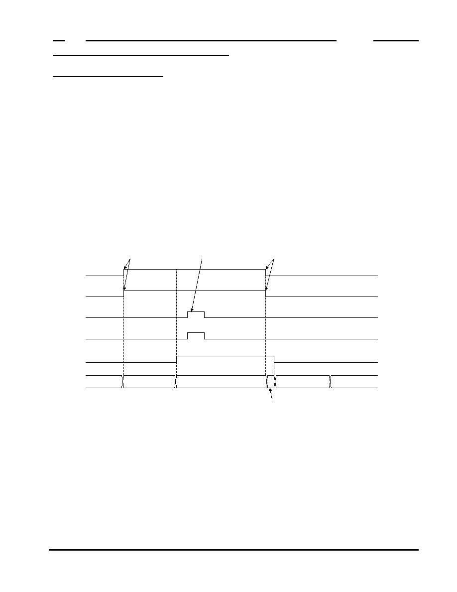
1.2 Phrase 1 Playback Operation
(1)
Input a "H" pulse to the PLAY1 pin to power up and start playback from the top address of the
memory.
(2)
The LSI automatically ends playback when the last address of the recorded phrase has been
reached.
(3)
The LSI automatically shifts to low-power consumption mode after playback ends.
(4)
To stop playback of phrase 1 before reaching the last address, input a "H" pulse again to
the PLAY1 or PLAY2 pin. This will cause the LSI to stop playback and then automatically
shift to low-power consumption mode.
(5)
During playback operation signal input to the PLAY1 or PLAY2 pin only is valid, any other
signal input is disregarded
Figure 1.2 Timing Chart for Phrase 1 Playback Operation
1.3 Phrase 1 Erasing Operation
(1)
While inputting "H" level to the ERASE pin, input a "H" pulse to the REC1 pin to start erasing
Phrase 1.
(2)
After Phrase 1 having been erased, the LSI automatically shifts to power-down mode for
low-power consumption.
Note: Erasing operation cannot be abandoned in the middle once getting started.
Internally, the LSI performs erasing Phrase 1 by recording "Silence" from the top address
to address 250. Therefore, if you attempt to playback the erased phrase, the playback
starts at the top address of the memory and ends at address 250.
Figure 1.3 Timing Chart for Phrase 1 Erasing Operation
Start Pulse
Stop Pulse
Power Down
Powering Up
Playing Back
Power Down
Powering Down
MON
PLAY2
PLAY1
Status
Start Pulse
Power Down
Powering Up
Erasing
Power Down
Powering Down
MON
REC1
ERASE
Status

OKI
ML2502
ML2502 Data Sheet (Revision 8.0)
6
1.4 Phrase 2 Recording Operation
(1)
Keep on inputting "H" level to the REC2 pin to power up and start recording from the top
address of the memory. Recording goes on while the REC2 pin being held "H" level.
(2)
The LSI automatically ends recording when the last address of the memory has been
reached.
(3)
The LSI automatically shifts to low-power consumption mode after recording ends.
(4)
To stop recording for Phrase 2 before reaching the last address, bring the REC2 pin down
to "L" level. The LSI automatically shifts to low-power consumption mode after recording
stops.
(5)
During recording operation any signal input to other pins than the REC2 is disregarded.
Note: Re-recording always causes to overwrite the existing recording data for a given phrase.
Figure 1.4 Timing Chart for Phrase 2 Recording Operation
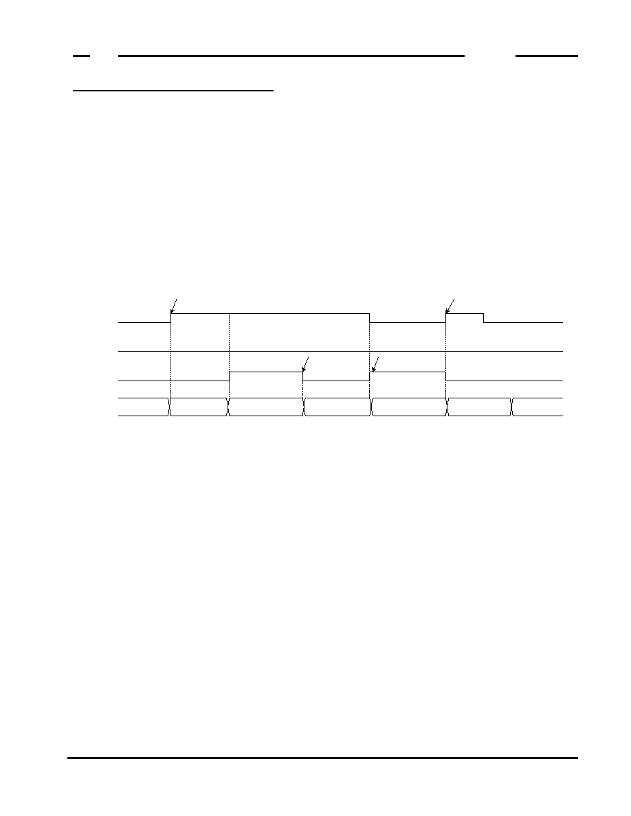
1.5 Phrase 2 Playback Operation
(1)
Input a "H" pulse to the PLAY2 pin to power up and start playback from the center address of
the memory.
(2)
The LSI automatically ends playback when the last address of the recorded phrase has been
reached.
(3)
The LSI automatically shifts to low-power consumption mode after playback ends.
(4)
To stop playback of Phrase 2 before reaching its last address, input a "H" pulse again to the
PLAY1 or PLAY2 pin. This will cause the LSI to stop playback and then automatically shift
to low-power consumption mode.
(5)
During playback operation signal input to the PLAY1 or PLAY2 pin only is valid, any other
signal input is disregarded
Figure 1.5 Timing Chart for Phrase 2 Playback Operation
Start
Stop
Invalid Input
Stopping Process
Power Down
Powering Up
Recording
Power Down
Powering Down
MON
REC2
REC1
Status
Start Pulse
Stop Pulse
Power Down
Powering Up
Playing Back
Power Down
Powering Down
MON
PLAY2
PLAY1
Status
Stop

OKI
ML2502
ML2502 Data Sheet (Revision 8.0)
7
1.6 Phrase 2 Erasing Operation
(1)
While inputting "H" level to the ERASE pin, input a "H" pulse to the REC2 pin to start erasing
Phrase 2.
(2)
After Phrase 2 having been erased, the LSI automatically shifts to power-down mode for
low-power consumption.
Note: Erasing operation cannot be abandoned in the middle once getting started.
Internally, the LSI performs erasing Phrase 2 by recording "Silence" from the center
address as far as to address 250. Therefore, if you attempt to playback the erased
phrase, the playback starts at the center address of the memory and ends at address 250.
Figure 1.6 Timing Chart for Phrase 2 Erasing Operation
Start Pulse
Power Down
Powering Up
Erasing
Power Down
Powering Down
MON
REC2
ERASE
Status
OKI
ML2502
ML2502 Data Sheet (Revision 8.0)
8
2. Single-phrase Record/Playback Mode
2.1 Recording Operation
(1)
In this mode the REC1 has to be connected with the REC2 pin.
Keep on inputting "H" level to the REC1 and the REC2 pin to power up and start recording
from the top address of the memory. Recording goes on while the REC1 and the REC2 pin
being held at "H" level.
(2)
The LSI automatically ends recording when the last address of the memory has been
reached.
(3)
The LSI automatically shifts to low-power consumption mode after recording ends.
(4)
To stop recording before reaching the last address, bring the REC1 and the REC2 pin down
to "L" level. The LSI automatically shifts to low-power consumption mode after recording
stops.
(5)
During recording operation any signal input to other pins than the REC1 and the REC2 is
disregarded.
Note: Re-recording always causes to overwrite the existing recording data for a given phrase.
Figure 2.1 Timing Chart for Single-phrase Recording Operation
Start
Stop
Invalid Input
Stopping Process
Power Down
Powering Up
Recording
Power Down
Powering Down
MON
REC2
REC1
Status
PLAY2
PLAY1

OKI
ML2502
ML2502 Data Sheet (Revision 8.0)
9
2.2 Playing Back Operation
(1)
Input "H" pulses to the PLAY1 and the PLAY2 pins simultaneously to power up and start
playback from the top address of the memory.
(2)
The LSI automatically ends playback when the last address of the recorded phrase has been
reached.
(3)
The LSI automatically shifts to low-power consumption mode after playback ends.
(4)
To stop playback of the phrase before reaching its last address, input "H" pulses again to the
PLAY1 and the PLAY2 pins simultaneously. This will cause the LSI to stop playback and
then automatically shift to low-power consumption mode.
(5)
During playback operation signal input to the PLAY1 or PLAY2 pin only is valid, any other
signal input is disregarded.
Figure 2.2 Timing Chart for Single-phrase Playback Operation
Start Pulse
Stop Pulse
Invalid Input
Power Down
Powering Up
Playing Back
Power Down
Powering Down
MON
REC2
REC1
Status
PLAY2
PLAY1

OKI
ML2502
ML2502 Data Sheet (Revision 8.0)
10
2.3 Erasing the Phrase 2
(1)
While inputting "H" level to the ERASE pin, input "H" pulses to the REC1 and REC2 pins
simultaneously to start erasing the phrase.
(2)
After the phrase having been erased, the LSI automatically shifts to power-down mode for
low-power consumption.
Note: Erasing operation cannot be abandoned in the middle once getting started.
Internally, the LSI performs erasing by recording "Silence" from the top address as far as to
address 250. Therefore, if you attempt to playback the erased phrase, the playback starts
at the top address of the memory and ends at address 250.
Figure 2.3 Timing Chart for Single-phrase Erasing Operation
Start Pulse
Power Down
Powering Up
Erasing
Power Down
Powering Down
MON
REC1
ERASE
Status
REC2
OKI
ML2502
ML2502 Data Sheet (Revision 8.0)
11
3. Repeating Playback Operation
(1)
To repeat playback of the same phrase, keep on inputting "H" level to the PLAY1 or PLAY2
pin. "H" level input to the PLAY1 or PLAY2 causes the LSI to power up and start playback.
(2)
The LSI automatically restarts playback when the last address of the phrase has been
reached.
(3)
When the playback reaches to the last address of the phrase, with the PLAY1 or PLAY2 pin
being held "L" level, the LSI automatically ends playback.
(4)
The LSI automatically powers down after playback ends.
(5)
To stop playback before repetitive playback session ends, bring the PLAY1 or PLAY2 pin
down to "L" level once, and then re-input a "H" pulse to the PLAY1 or PLAY2 pin. The LSI
automatically shifts to low-power consumption mode after playback stops.
Figure 3.1 Timing Chart for Repetitive Playback Operation
Start Pulse
Stop Pulse
Power Down Powering Up
Playing Back
Power Down
Powering Down
MON
PLAY2
PLAY1
Status
Interval
Playing Back
End Playing
Resume Plaing

OKI
ML2502
ML2502 Data Sheet (Revision 8.0)
12
n
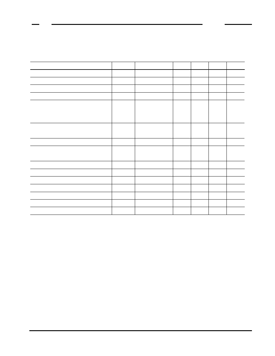
ABSOLUTE MAXIMUM RATINGS
n
RECOMMENDED OPERATING RANGES
n
ELECTRICAL CHARACTERISTICS
∑
DC Characteristics
Note:
1. Applicable only to those input pins without a pull-down resistor.
2. Applicable only to those input pins with a pull-down resistor. (REC1, REC2, PLAY1,
PLAY2, ERASE pins)
Parameter
Symbol
Conditions
Unit
V
DD
T
OP
DGND=AGND=0V
V
∞C
Range
Power Supply Voltage
Operating Temperature
2.7 ~ 3.3
-10 ~ + 70
--
Parameter
Symbol
Conditions
Unit
V
DD
T
STG
Ta = 25∞C
--
V
∞C
Rating
Power Supply Voltage
Storage Temperature
-0.3 ~ +6.0
-0.3 ~ V
DD
+ 0.3
Input Voltage
V
IN
V
-55 ~ +150
Parameter
Symbol
Conditions
Unit
Max.
Typ.
Min.
V
IH
DGND=AGND=0V
"L" Input Voltage
"H" Input Voltage
--
--
--
0.45
40
10
TBD
--
0.8 X
V
DD
-10
10
V
V
mA
--
I
OH
=40
µA
I
OL
=2mA
SPOUT Output
No Load
V
IL
=0V
V
IH
=V
DD
DV
DD
=AV
DD
=2.7V ~ 3.3V,DGND=AGND=0V,Ta= -10 ~ +70∞C
"L" Output Voltage
"H" Output Voltage
"L" Input Current *
1
"H" Input Current *
1
Operating Current
Consumption
Powerdown Current
Consumption
V
IL
V
OH
V
OL
I
IH1
I
IL1
I
DD
I
DDS1
µA
0.2 X V
DD
--
V
DD
- 0.3
µA
V
V
--
µA
µA
100
--
"L" Input Current *
2
"H" Input Current *
2
I
IH2
I
IL2
I
DDS2
Ta= -10 ~ +50∞C
Ta= +50 ~ +70∞C
µA
µA
100
V
IL
=0V
V
IH
=3.0V
10
-10
--
--
--
--
--
--
--
--
--
--
--
--
--

OKI
ML2502
ML2502 Data Sheet (Revision 8.0)
13
∑
AC Characteristics
Note:
*1. In proportion to sampling frequency.
Parameter
Symbol
Unit
Max.
Typ.
Min.
t
POR
Min. "H" Pulse Width for Record-Start Input
Power-on Reset Time
--
--
--
15.8
10
ms
DV
DD
=AV
DD
=2.7V ~ 3.3V,DGND=AGND=0V,Ta= -10 ~ +70∞C
t
W RECST
256
--
µs
µs
279
17
17
17
17
0
0
--
--
--
--
--
--
--
--
--
--
--
--
ms
ms
ms
ms
ms
ms
ms
ms
Min. "L" Pulse Width for Record-Stop Input
Setup Time for Erase Input - REC1, REC2 Input
Min. Pulse Width for Erase-Start Input to REC1,REC2
Min. Pulse Width for Playback-Start Input
Min. Pulse Width for Playback-Stop Input
Powering Up Time 1 (at Erasing)
Powering Up Time 2
Max. Record/Playback Time Length (2-phrase mode) *1
Max. Record/Playback Time Length (1-phrase mode) *1
Erase Execution Time *1
Max. Time for MON to Fall Down at Stop Recording*1
Powering Down Time
ms
ms
s
s
16.5
16.5
10.5
21
56
15.6
256
15.6
15.6
10
20
54
15.4
252
14.8
14.8
9.5
19
52
At fsamp = 6.4 kHz
t
W RECSP
t
W PLYST
t
W PLYSP
t
WERSST
t
WERSS
t
W ERSH
t
WS1
t
WS12
t
W S3
t
W S4
t
WRP2
t
WRP1
t
W E
Hold Time for Erase Input - REC1, REC2 Input
OKI
ML2502
ML2502 Data Sheet (Revision 8.0)
14
∑
Analog Circuit Characteristics
Parameter
Symbol
Conditions
Unit
Max.
Typ.
Min.
R
MIN
MIN Input Resistance
--
7.8
--
1.45
40
±125
--
k
V/V
mA
--
t
WS12 and
t
WS4
No Signal Playback
DV
DD
=AV
DD
=2.7V ~ 3.3V,DGND=AGND=0V,Ta= -10 ~ +70∞C
V
MOTP
V
28
--
VDD-0.25
V
M
dB
--
dB
--
V
V
±0.3
--
I
OL
= 10mA
--
--
40
0.95
--
200
--
--
V
LOTP
V
AOTP
1.35
1.25
Output Voltage from MOUT, LOUT,
AOUT on Powering Up and Powering
Down
6
4.2
--
LIN Input Impedance
Line Amp. Open-loop Gain
Mic. Amp. Voltage Gain Control Range
f
IN
= 0~4kHz
8
1
R
IOP
G
MIC
G
OLINE
Output Voltage from SPOUT +/-
on Powering Up and Powering Down
MOUT- LOUT Load Resistance
SPOUT+ / SPOUT-
Amplifier Open-loop Gain
SPOUT+/SPOUT- Voltage Gain
SPOUT +/- Output "H" Voltage
SPIN Input Impedance
SPOUT +/- Output "L" Voltage
SPOUT Output Load Impedance
SPOUT Output Offset Voltage
SPOUT Load Current at Peak Output
f
IN
= 0~4kHz
--
--
--
1/2 VDD
1/2 VDD
+0.1
1/2 VDD
-0.1
--
--
I
OH
= 10mA
1
1
--
16
--
--
--
--
--
--
0.25
--
--
--
1.05
V
M
V/V
k
V
SPOTP
V
SNOTP
R
OOP
G
OSP
G
SPC
R
ISP
V
SPH
V
SPL
V
OFF
R
SPC
I
SPO
t
WS12 and
t
WS4
OKI
ML2502
ML2502 Data Sheet (Revision 8.0)
15
n
TIMING CHARTS
u
Digital Circuit Section
∑
Powering Up
∑
Start Recording Phrase 1
∑
End Recording Phrase 1 (Recording reaches to the last address)
2.5V
VDD
Internal
Reset Signal
Status
Unstable State
Reseting
Power Down State
t
POR
Switch Input Allowed
Power Down State
Powering Up Time
Recording
MON
REC2
REC1
Status
t
WRECST
t
WS12
t
W RP1,tWRP2
Powering Down
Power Down State
Recording
MON
REC2
REC1
Status
t
WS4
t
WRP1,
t
WRP2

OKI
ML2502
ML2502 Data Sheet (Revision 8.0)
16
∑
Stop Recording Phrase 1 (Recording stopped before the last address)
∑
Start Playback Phrase 1
∑
End Playback Phrase 1 (Playback reaches to the last address)
Power Down State
Powering Up Time
Playing Back
MON
PLAY2
PLAY1
Status
t
W PLYST
t
WS12
t
WRP1,
t
W RP2
Powering Down
Power Down State
Playing Back
MON
PLAY2
PLAY1
Status
t
WS4
t
WRP1,
t
W RP2
Post-Recording Process
Power Down State
Recording
MON
REC2
REC1
Status
t
WS3
Powering Down
t
WS4
t
W RECSP
OKI
ML2502
ML2502 Data Sheet (Revision 8.0)
17
∑
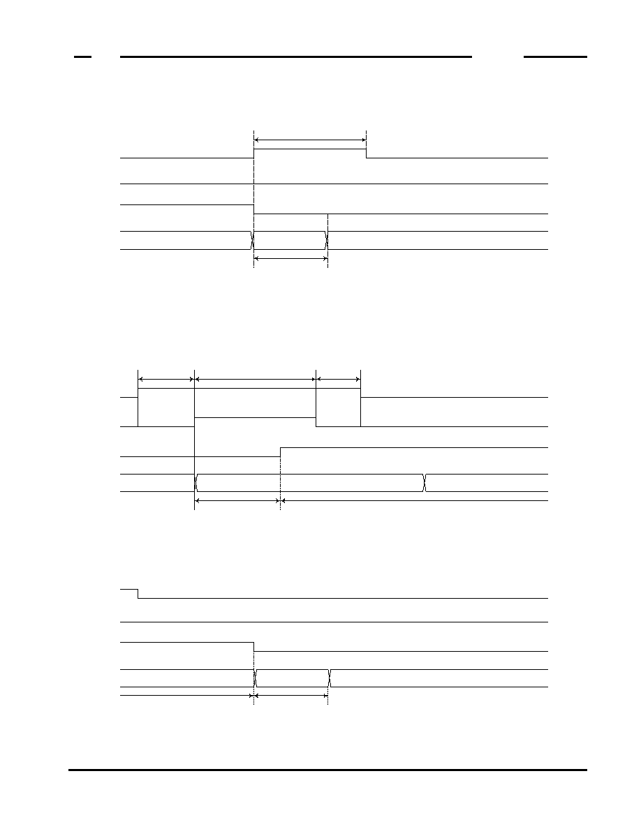
Stop Playback Phrase1 (Recording stopped before the last address)
∑
Start Erasing Phrase 1
∑
End Erasing Phrase 1
Powering Down
Power Down State
Playing Back
MON
PLAY2
PLAY1
Status
t
W S4
t
W PLYSP
Power Down State
Powering Up Time
Erasing
MON
REC1
ERASE
Status
t
WERSST
t
WS1
t
W E
t
WERSS
t
WERSH
Powering Down
Power Down State
Erasing
MON
ERASE
REC1
Status
t
WS4
t
W E

OKI
ML2502
ML2502 Data Sheet (Revision 8.0)
18
u
Analog Circuit Section
∑
Start Recording (Phrase 1)
∑
Stop Recording (Phrase 1)
MON
REC1
MOUT
LOUT
AOUT
SPOUT+
SPOUT-
Status
V
LOTP
V
MOTP
GND Level
GND Level
GND Level
Hi-Z
Hi-Z
t
WS12
Power Down
Powering UP
Recording
AOUT
SPOUT+
SPOUT-
Status
GND Level
Hi-Z
Hi-Z
t
WS3
Post-Recording Process
Powering Down
Recording
MON
REC1
MOUT
LOUT
PowerDown
GND Level
GND Level
t
WS4
V
LOTP
V
MOTP

OKI
ML2502
ML2502 Data Sheet (Revision 8.0)
19
∑
Start Playback (Phrase 1)
∑
Stop Playback (Phrase 1)
MON
PLAY1
MOUT
LOUT
AOUT
SPOUT+
SPOUT-
Status
V
AOTP
GND Level
GND Level
GND Level
Hi-Z
Hi-Z
t
WS12
Power Down
Powering UP Time
Playing Back
V
SPOTP
V
SNOTP
MON
PLAY1
MOUT
LOUT
GND Level
GND Level
AOUT
SPOUT+
SPOUT-
Status
Powering Down
Playing Back
Power Down State
t
WS4
V
AOTP
V
SPOTP
V
SNOTP
GND Level
Hi-Z
Hi-Z

OKI
ML2502
ML2502 Data Sheet (Revision 8.0)
20
n
Application Circuit Sample
Single-phrase Record/Playback, at 4 kHz sampling frequency and with a Dynamic Speaker.
1
2
3
4
5
11
12
13
14
15
6
7
8
9
10
30
29
28
27
26
20
19
18
17
16
25
24
23
22
21
NC
DVDD
REC1
REC2
PLAY1
PLAY2
ERASE
MIN
MOUT
LIN
LOUT
AVDD
AVDD
SPOUT+
NC
NC
SAM1
SAM2
ROSC
DGND
MON
TEST
NC
NC
AOUT
SPIN
AGND
SPOUT-
AGND
NC
ML2502
MIC
LED
Speaker