
TL F 5886
MM54C85MM74C85
4-Bit
Magnitude
Comparator
September 1989
MM54C85 MM74C85 4-Bit Magnitude Comparator
General Description
The MM54C85 MM74C85 is a four-bit magnitude compara-
tor which will perform comparison of straight binary or BCD
codes The circuit consists of eight comparing inputs (A0
A1 A2 A3 B0 B1 B2 B3) three cascading inputs (A
l
B
A
k
B and A
e
B) and three outputs (A
l
B A
k
B and
A
e
B) This device compares two four-bit words (A and B)
and determines whether they are ``greater than '' ``less
than '' or ``equal to'' each other by a high level on the appro-
priate output For words greater than four-bits units can be
cascaded by connecting the outputs (A
l
B A
k
B and
A
e
B) of the least significant stage to the cascade inputs
(A
l
B A
k
B and A
e
B) of the next-significant stage In
addition the least significant stage must have a high level
voltage (V
IN(1)
) applied to the A
e
B input and low level
voltage (V
IN(0)
) applied to A
l
B and A
k
B inputs
Features
Y
Wide supply voltage range
3 0V to 15V
Y
Guaranteed noise margin
1 0V
Y
High noise immunity
0 4 V
CC
(typ )
Y
Low power
fan out of 2
TTL compatibility
driving 74L
Y
Expandable to `N' stages
Y
Applicable to binary or BCD
Y
Low power pinout 54L85 74L85
Logic Diagram
TL F 5886 � 1
C1995 National Semiconductor Corporation
RRD-B30M105 Printed in U S A

Absolute Maximum Ratings
(Note 1)
If Military Aerospace specified devices are required
please contact the National Semiconductor Sales
Office Distributors for availability and specifications
Voltage at Any Pin
b
0 3V to V
CC
a
0 3V
Operating Temperature Range
MM54C85
b
55 C to
a
125 C
MM74C85
b
40 C to
a
85 C
Storage Temperature Range
b
65 C to
a
150 C
Power Dissipation (P
D
)
Dual-In-Line
700 mW
Small Outline
500 mW
Operating V
CC
Range
3 0V to 15V
V
CC
18V
Lead Temperature
(Soldering 10 seconds)
260 C
DC Electrical Characteristics
Min Max limits apply across temperature range unless otherwise noted
Symbol
Parameter
Conditions
Min
Typ
Max
Units
CMOS TO CMOS
V
IN(1)
Logical ``1'' Input Voltage
V
CC
e
5 0V
3 5
V
V
CC
e
10V
8 0
V
V
IN(0)
Logical ``0'' Input Voltage
V
CC
e
5 0V
1 5
V
V
CC
e
10V
2 0
V
V
OUT(1)
Logical ``1'' Output Voltage
V
CC
e
5 0V I
O
e b
10 mA
4 5
V
V
CC
e
10V I
O
e b
10 mA
9 0
V
V
OUT(0)
Logical ``0'' Output Voltage
V
CC
e
5 0V I
O
e a
10 mA
0 5
V
V
CC
e
10V I
O
e a
10 mA
1 0
V
I
IN(1)
Logical ``1'' Input Current
V
CC
e
15V V
IN
e
15V
0 005
1 0
m
A
I
IN(0)
Logical ``0'' Input Current
V
CC
e
15V V
IN
e
0V
b
1 0
b
0 005
m
A
I
CC
Supply Current
V
CC
e
15V
0 05
300
m
A
CMOS LPTTL INTERFACE
V
IN(1)
Logical ``1'' Input Voltage
54C V
CC
e
4 5V
V
CC
b
1 5
V
74C V
CC
e
4 75V
V
CC
b
1 5
V
V
IN(0)
Logical ``0'' Input Voltage
54C V
CC
e
4 5V
0 8
V
74C V
CC
e
4 75V
0 8
V
V
OUT(1)
Logical ``1'' Output Voltage
54C V
CC
e
4 5V I
O
e b
360 mA
2 4
V
74C V
CC
e
4 75V I
O
e b
360 mA
2 4
V
V
OUT(0)
Logical ``0'' Output Voltage
54C V
CC
e
4 5V I
O
e
360 mA
0 4
V
74C V
CC
e
4 75V I
O
e
360 mA
0 4
V
OUTPUT DRIVE (See 54C 74C Family Characteristics Data Sheet) (Short Circuit Current)
I
SOURCE
Output Source Current
V
CC
e
5 0V V
OUT
e
0V
b
1 75
b
3 3
mA
(P-Channel)
T
A
e
25 C
I
SOURCE
Output Source Current
V
CC
e
10V V
OUT
e
0V
b
8 0
b
15
mA
(P-Channel)
T
A
e
25 C
I
SINK
Output Sink Current
V
CC
e
5 0V V
OUT
e
V
CC
1 75
3 6
mA
(N-Channel)
T
A
e
25 C
I
SINK
Output Sink Current
V
CC
e
10V V
OUT
e
V
CC
8 0
16
mA
(N-Channel)
T
A
e
25 C
AC Electrical Characteristics
T
A
e
25 C C
L
e
50 pF unless otherwise specified
Symbol
Parameter
Conditions
Min
Typ
Max
Units
t
pd
Propagation Delay from any A
V
CC
e
50V
250
600
ns
or B Data Input to any
V
CC
e
10V
100
300
ns
Data Output
t
pd
Propagation Delay Time from
V
CC
e
50V
200
500
ns
any Cascade Input to
V
CC
e
10V
100
250
ns
any Output
C
IN
Input Capacitance
Any Inupt
5 0
pF
C
PD
Power Dissipation Capacitance
(Note 3) Per Package
45
pF
AC Parameters are guaranteed by DC correlated testing
Note 1
``Absolute Maximum Ratings'' are those values beyond which the safety of the device cannot be guaranteed Except for ``Operating Temperature Range''
they are not meant to imply that the devices should be operated at these limits The table of ``Electrical Characteristics'' provides conditions for actual device
operation
Note 2
Capacitance is guaranteed by periodic testing
Note 3
C
PD
determines the no load AC power consumption of any CMOS device For complete explanation see 54C 74C Family Characteristics application note
AN-90
2

Typical Applications
Four Digit Comparator
TL F 5886 � 2
Connection Diagram
Dual-In-Line Package
TL F 5886 � 3
Top View
Order Number MM54C85
or MM74C85
Switching Time
Waveforms
TL F 5886 � 4
Unused inputs must be tied
to an appropriate logic level
Truth Table
Comparing Inputs
Cascading Inputs
Outputs
A3 B3
A2 B2
A1 B1
A0 B0
A
l
B
A
k
B
A
e
B
A
l
B
A
k
B
A
e
B
A3
l
B3
X
X
X
X
X
X
H
L
L
A3
k
B3
X
X
X
X
X
X
L
H
L
A3
e
B3
A2
l
B2
X
X
X
X
X
H
L
L
A3
e
B3
A2
k
B2
X
X
X
X
X
L
H
L
A3
e
B3
A2
e
B2
A1
l
B1
X
X
X
X
H
L
L
A3
e
B3
A2
e
B2
A1
k
B1
X
X
X
X
L
H
L
A3
e
B3
A2
e
B2
A1
e
B1
A0
l
B0
X
X
X
H
L
L
A3
e
B3
A2
e
B2
A1
e
B1
A0
k
B0
X
X
X
L
H
L
A3
e
B3
A2
e
B2
A1
e
B1
A0
e
B0
H
L
L
H
L
L
A3
e
B3
A2
e
B2
A1
e
B1
A0
e
B0
L
H
L
L
H
L
A3
e
B3
A2
e
B2
A1
e
B1
A0
e
B0
L
L
H
L
L
H
A3
e
B3
A2
e
B2
A1
e
B1
A0
e
B0
L
H
H
L
H
H
A3
e
B3
A2
e
B2
A1
e
B1
A0
e
B0
H
L
H
H
L
H
A3
e
B3
A2
e
B2
A1
e
B1
A0
e
B0
H
H
H
H
H
H
A3
e
B3
A2
e
B2
A1
e
B1
A0
e
B0
H
H
L
H
H
L
A3
e
B3
A2
e
B2
A1
e
B1
A0
e
B0
L
L
L
L
L
L
H
e
high level L
e
low level X
e
irrelevant
3
MM54C85MM74C85
4-Bit
Magnitude
Comparator
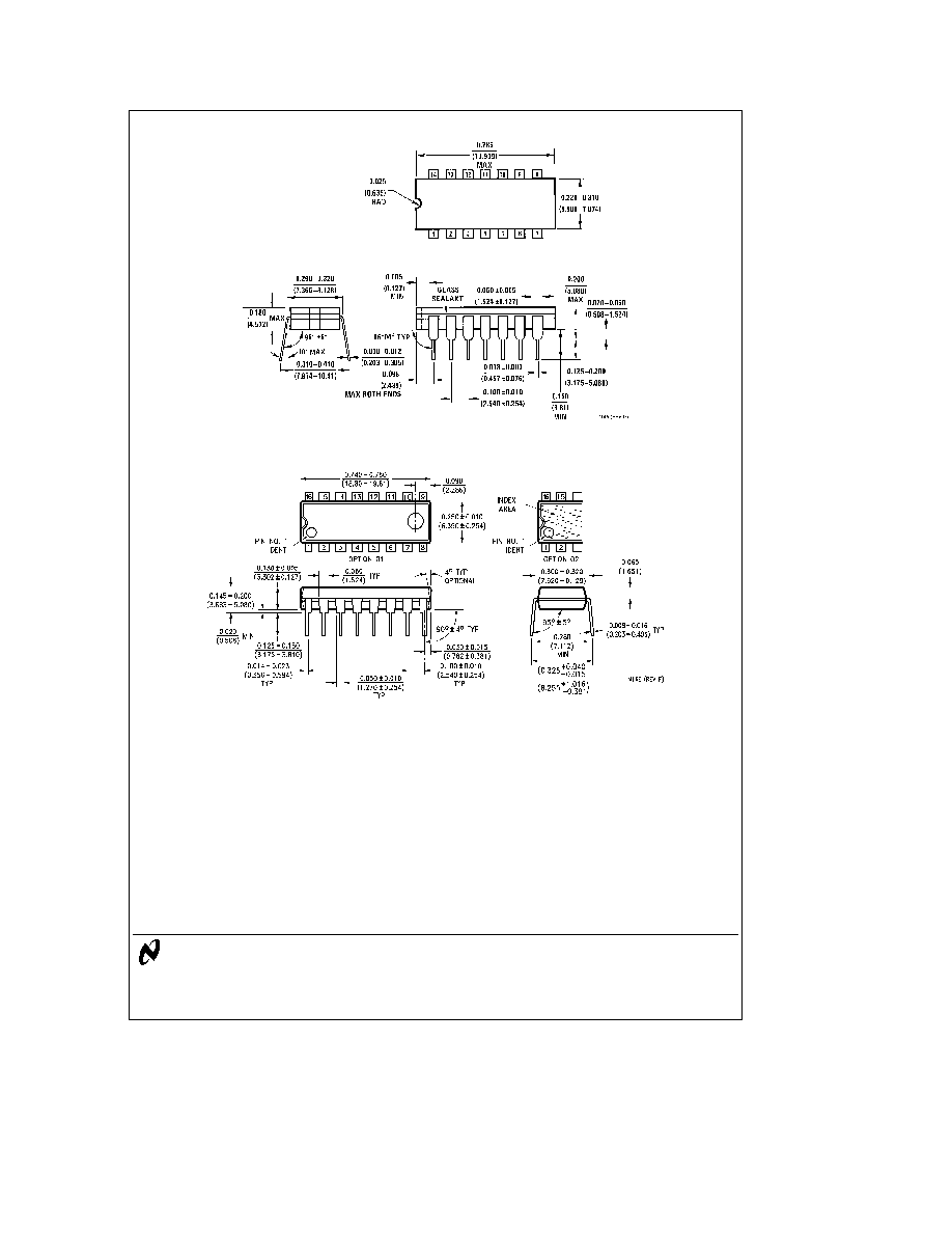
Physical Dimensions
inches (millimeters)
Ceramic Dual-In-Line Package (J)
Order Number MM54C85J or MM74C85J
NS Package Number J14A
Molded Dual-In-Line Package (N)
Order Number MM54C85N or MM74C85N
NS Package Number N16E
LIFE SUPPORT POLICY
NATIONAL'S PRODUCTS ARE NOT AUTHORIZED FOR USE AS CRITICAL COMPONENTS IN LIFE SUPPORT
DEVICES OR SYSTEMS WITHOUT THE EXPRESS WRITTEN APPROVAL OF THE PRESIDENT OF NATIONAL
SEMICONDUCTOR CORPORATION As used herein
1 Life support devices or systems are devices or
2 A critical component is any component of a life
systems which (a) are intended for surgical implant
support device or system whose failure to perform can
into the body or (b) support or sustain life and whose
be reasonably expected to cause the failure of the life
failure to perform when properly used in accordance
support device or system or to affect its safety or
with instructions for use provided in the labeling can
effectiveness
be reasonably expected to result in a significant injury
to the user
National Semiconductor
National Semiconductor
National Semiconductor
National Semiconductor
Corporation
Europe
Hong Kong Ltd
Japan Ltd
1111 West Bardin Road
Fax (a49) 0-180-530 85 86
13th Floor Straight Block
Tel 81-043-299-2309
Arlington TX 76017
Email cnjwge tevm2 nsc com
Ocean Centre 5 Canton Rd
Fax 81-043-299-2408
Tel 1(800) 272-9959
Deutsch Tel (a49) 0-180-530 85 85
Tsimshatsui Kowloon
Fax 1(800) 737-7018
English
Tel (a49) 0-180-532 78 32
Hong Kong
Fran ais Tel (a49) 0-180-532 93 58
Tel (852) 2737-1600
Italiano
Tel (a49) 0-180-534 16 80
Fax (852) 2736-9960
National does not assume any responsibility for use of any circuitry described no circuit patent licenses are implied and National reserves the right at any time without notice to change said circuitry and specifications