 | –≠–ª–µ–∫—Ç—Ä–æ–Ω–Ω—ã–π –∫–æ–º–ø–æ–Ω–µ–Ω—Ç: LMX2346 | –°–∫–∞—á–∞—Ç—å:  PDF PDF  ZIP ZIP |
LMX2346/LMX2347
PLLatinum
TM
Frequency Synthesizer for RF Personal
Communications
LMX2346
2.0 GHz
LMX2347
2.5 GHz
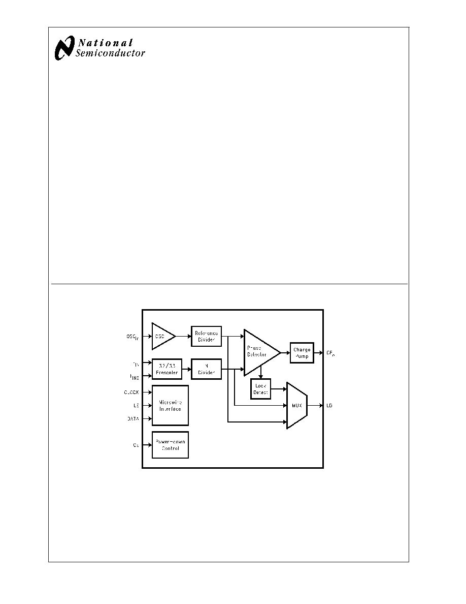
General Description
The LMX2346/7 are high performance frequency synthesiz-
ers with an integrated 32/33 dual modulus prescaler. The
LMX2346 is designed for RF operation up to 2.0 GHz. The
LMX2347 is designed for RF operation up to 2.5 GHz. Using
a proprietary digital phase locked loop technique, the
LMX2346/7 generates very stable, low noise control signals
for UHF and VHF voltage controlled oscillators.
Serial data is transferred into the LMX2346/7 via a three-line
MICROWIRE interface (DATA, LE, CLOCK). Supply voltage
range is from 2.7V to 5.5V. The charge pump provides 4 mA
output current.
The LMX2346/7 are manufactured using National's 0.5µ
ABiC V silicon BiCMOS process and is available in 16-pin
TSSOP and 16-pin CSP packages.
Features
n
RF operation up to 2.5 GHz
n
2.7V to 5.5V operation
n
Digital & Analog Lock Detect
n
32/33 Dual modulus prescaler
n
Excellent Phase Noise
n
Internal balanced, low leakage charge pump
n
Pin Compatible to LMX2323
Applications
n
Cellular DCS/PCS/3G infrastructure equipment
n
Wireless Local Area Networks (WLANs)
n
Other wireless communication systems
Functional Block Diagram
20038406
PLLatinum
TM
is a trademark of National Semiconductor Corporation.
June 2004
LMX2346/LMX2347
PLLatinum
Frequency
Synthesizer
for
RF
Personal
Communications
© 2004 National Semiconductor Corporation
DS200384
www.national.com

Connection Diagrams
20038407
16-Pin Chip Scale Package
NS Package Number SLB16A
20038401
16-Pin TSSOP Package
NS Package Number MTC16
Pin Descriptions
Pin Name
Pin Number
I/O
Description
I/O Circuit Configuration
16-Pin
CSP
16-Pin
TSSOP
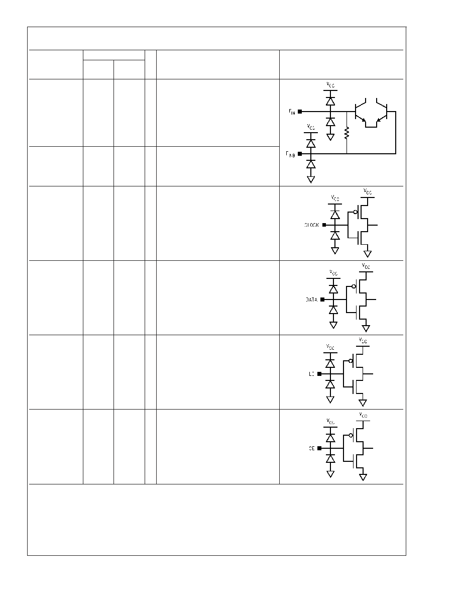
OSC
IN
15
1
I
Reference oscillator input. A CMOS
inverting gate input. The input has a
V
CC
/2 input threshold and can be driven
from an external CMOS or TTL logic
gate.
V
P
1
3
-- Charge Pump Power Supply. Must be
V
CC
.
V
CC
2
4
-- Main Power Supply. V
CC
may range from
2.7V to 5.5V. Bypass capacitors should
be placed as close as possible to this pin
and be connected directly to the ground
plane.
CP
o
3
5
O Charge Pump output. For connection to a
loop filter for driving the voltage control
input of an external VCO.
GND
4
6
-- Ground.
LMX2346/LMX2347
www.national.com
2
Pin Descriptions
(Continued)
Pin Name
Pin Number
I/O
Description
I/O Circuit Configuration
16-Pin
CSP
16-Pin
TSSOP
F
INB
5
7
I
RF prescaler complementary input. For
single ended operation, this pin should be
AC grounded. The LMX2346/7 can be
driven differentially when a bypass
capacitor is omitted.
F
IN
6
8
I
RF PLL prescaler input. Small signal
input from the VCO.
CLOCK
8
9
I
High impedance CMOS Clock input. Data
is clocked in on the rising edge, into the
18-bit shift register.
DATA
9
10
I
Binary serial data input. Data entered
MSB first. LSB is control bit. High
impedance CMOS input.
LE
10
11
I
Latch Enable input. When Latch Enable
transitions HIGH, data stored in the 18-bit
shift register is loaded into one of the 2
control registers, based on the address
bit. High impendance CMOS input.
CE
11
12
I
Chip Enable input. Provides logical
power-down control of the device. Pull-up
to V
CC
if unused. High impedance CMOS
input.
LMX2346/LMX2347
www.national.com
3
Pin Descriptions
(Continued)
Pin Name
Pin Number
I/O
Description
I/O Circuit Configuration
16-Pin
CSP
16-Pin
TSSOP
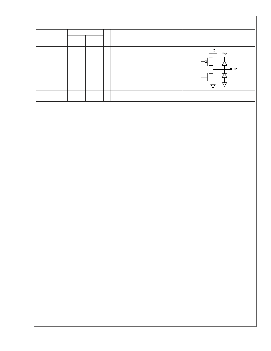
LD
13
14
O Locked Detect output. Multi-function
CMOS output pin that provides
multiplexed access to digital lock detect,
open-drain analog lock detect, as well as
the outputs of the R and N counters.
NC
7, 12, 14,
16
2, 13, 15,
16
No Connect.
LMX2346/LMX2347
www.national.com
4
Absolute Maximum Ratings
(Notes 1,
2)
If Military/Aerospace specified devices are required,
please contact the National Semiconductor Sales Office/
Distributors for availability and specifications.
Power Supply Voltage,
(V
CC
)
-0.3V to +6.5V
Power Supply for Charge
Pump,
(V
P
)
-0.3V to +6.5V
Voltage on any pin with
GND=0V, except V
P
(V
i
)
-0.3V to V
CC
+0.3V
Storage Temperature
Range, (T
S
)
-65∞C to +150∞C
Lead Temp. (solder 4 sec.),
(T
L
)
+260∞C
Recommended Operating
Conditions
(Note 1)
Min Max Unit
Power Supply Voltage, (V
CC
)
2.7
5.5
V
Power Supply for Charge Pump, (V
P
)
V
CC
6.0
V
Operating Temperature, (T
A
)
-40 +85
∞C
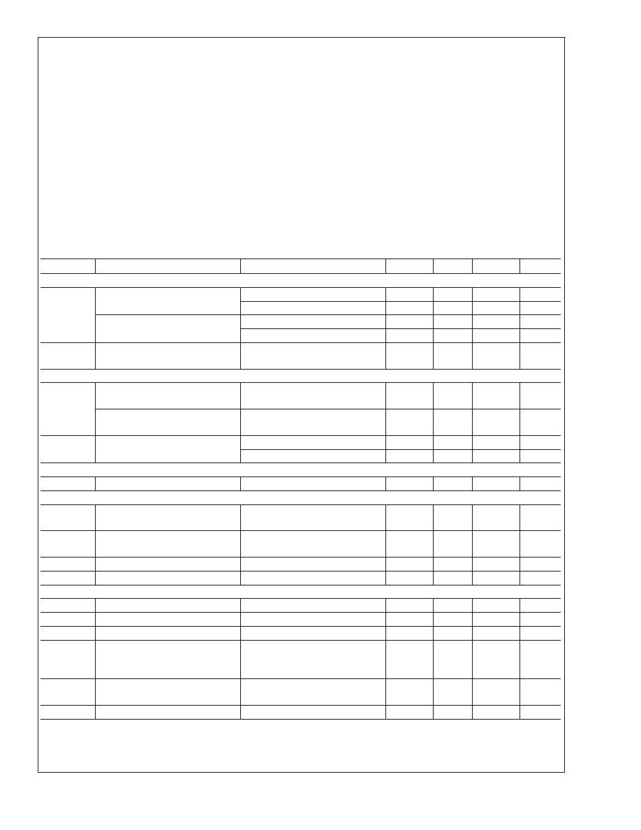
Electrical Characteristics
The following conditions apply; V
CC
= 3.0V, V
P
= 3.0V; -40∞C
T
A
85∞C, unless specified differently.
Symbol
Parameter
Conditions
Min
Typ
Max
Units
I
CC
I
CC
Power Supply Current, LMX2346
3.5
4.5
mA
V
CC
= 5.5V
7.0
mA
Power Supply Current, LMX2347
4.5
5.5
mA
V
CC
= 5.5V
8.0
mA
I
CC
-pwdn
Power Down Current
CLOCK, DATA, LE = GND
CE = GND
1
10
µA
RF PRESCALER
F
IN
Operating Frequency, RF
Prescaler, LMX2346
0.2
2.0
GHz
Operating Frequency, RF
Prescaler, LMX2347
0.2
2.5
GHz
PF
IN
Input Sensitivity, RF Prescaler
2.7V
V
CC
3.0V (Note 6)
-15
+0
dBm
3.0V
<
V
CC
5.5V (Note 6)
-10
+0
dBm
PHASE DETECTOR
F
Phase Detector Frequency
10
MHz
REFERENCE OSCILLATOR
F
OSC
Operating Frequency, Reference
Oscillator Input
(Note 10)
5
104
MHz
V
OSC
Input Sensitivity, Reference
Oscillator Input
(Note 7)
0.4
V
CC
- 0.3
V
PP
I
IH
OSC
in
High-Level Input Current
V
IH
= V
CC
= 5.5V
100
µA
I
IL
OSC
in
Low-Level Input Current
V
IL
= 0V, V
CC
= 5.5V
-100
µA
CHARGE PUMP
ICPo-
source
Charge Pump Source Current
VCPo = Vp/2V
-4.0
mA
ICPo-
sink
Charge Pump Sink Current
VCPo = Vp/2V
4.0
mA
ICPo-
tri
Charge Pump TRI-STATE Current
0.5V
VCPo V
P
- 0.5V
-2.5
2.5
nA
ICPo-
sink
vs.
ICPo-
source
CP Sink vs. Source Mismatch
VCPo = Vp/2
T
A
= 25∞
(Note 4)
3
10
%
ICPo vs
VCPo
CP Current vs. Voltage
0.5V
VCPo V
P
- 0.5V
T
A
= 25∞ (Note 4)
10
15
%
ICPo vs T
A
CP Current vs. Temperature
VCPo = Vp/2V (Note 4)
10
%
LMX2346/LMX2347
www.national.com
5