 | –≠–ª–µ–∫—Ç—Ä–æ–Ω–Ω—ã–π –∫–æ–º–ø–æ–Ω–µ–Ω—Ç: LMX1601 | –°–∫–∞—á–∞—Ç—å:  PDF PDF  ZIP ZIP |

LMX1600/LMX1601/LMX1602
PLLatinum
TM
Low Cost Dual Frequency Synthesizer
LMX1600
2.0 GHz/500 MHz
LMX1601
1.1 GHz/500 MHz
LMX1602
1.1 GHz/1.1 GHz
General Description
The LMX1600/01/02 is part of a family of monolithic inte-
grated dual frequency synthesizers designed to be used in a
local oscillator subsystem for a radio transceiver. It is fabri-
cated using National's 0.5u ABiC V silicon BiCMOS process.
The LMX1600/01/02 contains two dual modulus prescalers,
four programmable counters, two phase detectors and two
selectable gain charge pumps necessary to provide the con-
trol voltage for two external loop filters and VCO loops. Digi-
tal filtered lock detects for both PLLs are included. Data is
transferred into the LMX1600/01/02 via a MICROWIRE
TM
serial interface (Data, Clock, LE).
V
CC
supply voltage can range from 2.7V to 3.6V. The
LMX1600/01/02 features very low current consumption -
typically 4.0 mA at 3V for LMX1601, 5.0 mA at 3V for
LMX1600 or LMX1602. Powerdown for the PLL is hardware
controlled.
The LMX1600/01/02 is available in a 16 pin TSSOP surface
mount plastic package.
Features
n
V
CC
= 2.7V to 3.6V operation
n
Low current consumption:
4 mA
@
3V (typ) for LMX1601
5 mA
@
3V (typ) for LMX1600 or LMX1602
n
PLL Powerdown mode: I
CC
= 1 µA typical
n
Dual modulus prescaler:
-- 2 GHz/500 MHz option:
(Main) 32/33 (Aux) 8/9
-- 1.1 GHz/500 MHz option:
(Main) 16/17 (Aux) 8/9
-- 1.1 GHz/1.1 GHz option:
(Main) 16/17 (Aux) 16/17
n
Digital Filtered Lock Detects
Applications
n
Cordless / Cellular / PCS phones
n
Other digital mobile phones
Functional Block Diagram
TRI-STATE
Æ
is a registered trademark of National Semiconductor Corporation.
MICROWIRE
TM
and PLLatinum
TM
are trademarks of National Semiconductor Corporation.
DS100129-1
PRELIMINARY
March 1998
LMX1600/LMX1601/LMX1602
PLLatinum
Low
Cost
Dual
Frequency
Synthesizer
© 1998 National Semiconductor Corporation
DS100129
www.national.com
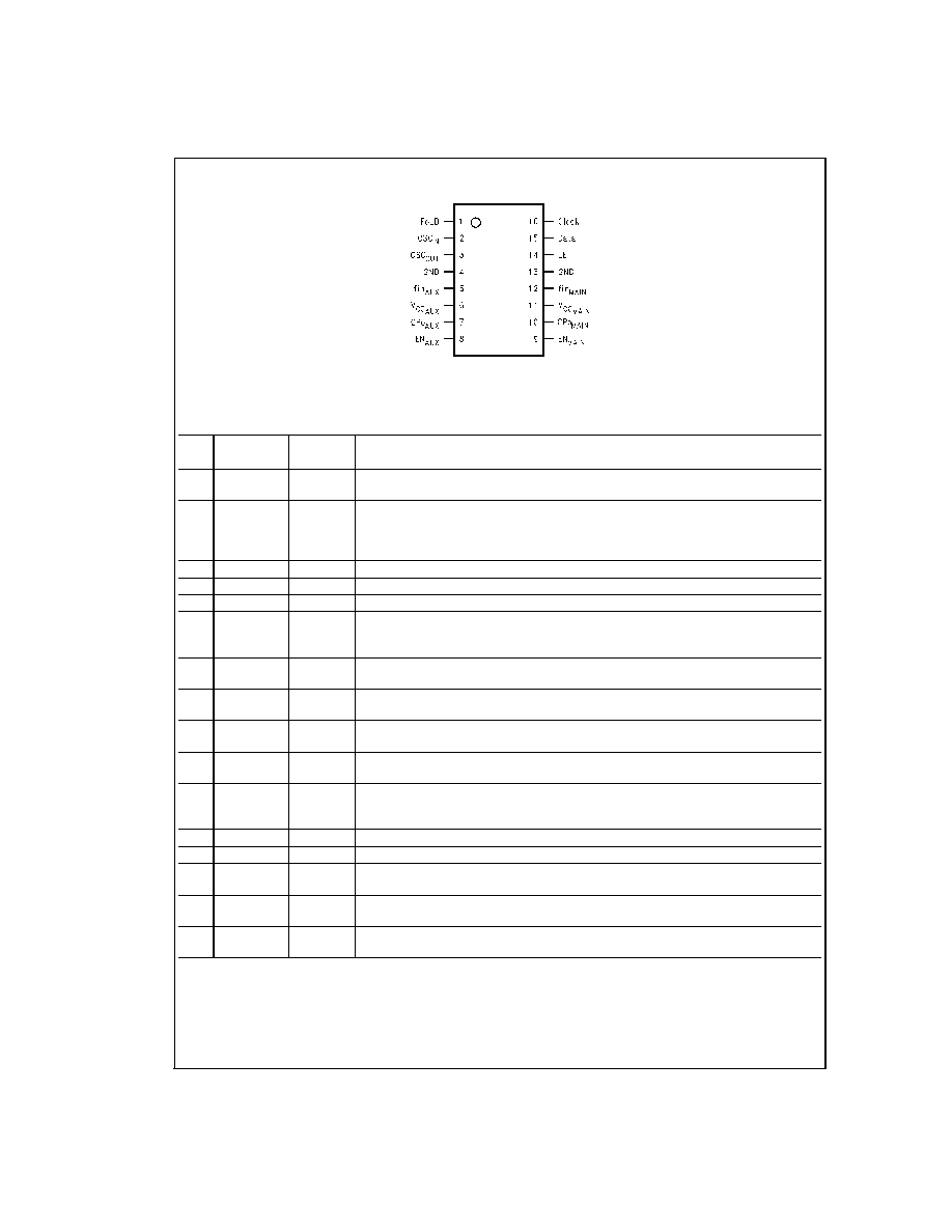
Connection Diagram
Pin Description
Pin
No.
Pin Name
I/O
Description
1
FoLD
O
Multiplexed output of the Main/Aux programmable or reference dividers and Main/Aux lock
detect. CMOS output. (See Programming Description 2.5)
2
OSC
IN
I
PLL reference input which drives both the Main and Aux R counter inputs. Has about 1.2V
input threshold and can be driven from an external CMOS or TTL logic gate. Typically
connected to a TCXO output. Can be used with an external resonator (See Programming
Description 2.5.4).
3
OSC
OUT
O
Oscillator output. Used with an external resonator.
4
GND
--
Aux PLL ground.
5
fin
AUX
I
Aux prescaler input. Small signal input from the VCO.
6
V
CCAUX
--
Aux PLL power supply voltage input. Must be equal to V
CCMAIN
. May range from 2.7V to
3.6V. Bypass capacitors should be placed as close as possible to this pin and be
connected directly to the ground plane.
7
CPo
AUX
O
Aux PLL Charge Pump output. Connected to a loop filter for driving the control input of an
external VCO.
8
EN
AUX
I
Powers down the Aux PLL when LOW (N and R counters, prescaler, and tristates charge
pump output). Bringing EN
AUX
HIGH powers up the Aux PLL.
9
EN
MAIN
I
Powers down the Main PLL when LOW (N and R counters, prescaler, and tristates charge
pump output). Bringing EN
MAIN
HIGH powers up the Main PLL.
10
CPo
MAIN
O
Main PLL Charge Pump output. Connected to a loop filter for driving the control input of an
external VCO.
11
V
CCMAIN
--
Main PLL power supply voltage input. Must be equal to V
CCAUX
. May range from 2.7V to
3.6V. Bypass capacitors should be placed as close as possible to this pin and be
connected directly to the ground plane.
12
fin
MAIN
I
Main prescaler input. Small signal input from the VCO.
13
GND
--
Main PLL ground.
14
LE
I
Load enable high impedance CMOS input. Data stored in the shift registers is loaded into
one of the 4 internal latches when LE goes HIGH (control bit dependent).
15
Data
I
High impedance CMOS input. Binary serial data input. Data entered MSB first. The last two
bits are the control bits.
16
Clock
I
High impedance CMOS Clock input. Data for the various counters is clocked in on the
rising edge, into the 18-bit shift register.
DS100129-2
Order Number LMX1600TM, LMX1601TM, or LMX1602TM
NS Package Number MTC16
www.national.com
2

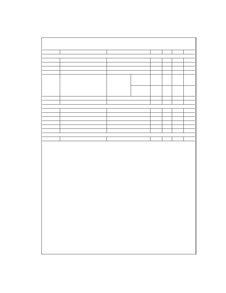
Absolute Maximum Ratings
(Notes 1, 2)
If Military/Aerospace specified devices are required, please contact the National Semiconductor Sales Office/
Distributors for availability and specifications.
Value
Parameter
Symbol
Min
Typical
Max
Unit
V
CCMAIN
-0.3
6.5
V
Power Supply Voltage
V
CCAUX
-0.3
6.5
V
Voltage on any pin with GND=0V
V
I
-0.3
V
CC
+ 0.3
V
Storage Temperature Range
T
S
-65
+150
∞C
Lead Temp. (solder 4 sec)
T
L
+260
∞C
ESD-Human Body Model (Note 2)
2000
eV
Recommended Operating Conditions
Value
Parameter
Symbol
Min
Typical
Max
Unit
V
CCMAIN
2.7
3.6
V
Power Supply Voltage
V
CCAUX
V
CCMAIN
V
CCMAIN
V
Operating Temperature
T
A
-40
+85
∞C
Note 1: "Absolute Maximum Ratings" indicate limits beyond which damage to the device may occur. Recommended Operating Conditions indicate conditions for
which the device is intended to be functional, but do not guarantee specific performance limits. Electrical Characteristics document specific minimum and/or maxi-
mum performance values at specified test conditions and are guaranteed. Typical values are for informational purposes only - based on design parameters or device
characterization and are not guaranteed.
Note 2: This device is a high performance RF integrated circuit and is ESD sensitive. Handling and assembly of this device should only be done on ESD-free work-
stations.
Electrical Characteristics
(V
CCMAIN
= V
CCAUX
= 3.0V; T
A
= 25∞C except as specified)
Symbol
Parameter
Conditions
Min
Typ
Max
Units
GENERAL
I
CC
Power
Supply
Current
2 GHz + 500 MHz
Crystal Mode (Note 3)
5.0
mA
1.1 GHz + 500 MHz
Crystal Mode (Note 3)
4.0
mA
1.1 GHz + 1.1 GHz
Crystal Mode (Note 3)
5.0
mA
2 GHz Only
Crystal Mode (Note 3)
3.5
mA
1.1 GHz Only
Crystal Mode (Note 3)
2.5
mA
500 MHz Only
Crystal Mode (Note 3)
1.5
mA
I
CC-PWDN
Power Down Current
EN
MAIN
= LOW, EN
AUX
= LOW
1
µA
fin
fin Operating Frequency
fin Main 2 GHz Option
200
2000
MHz
fin Main and Aux 1.1 GHz Option
100
1100
MHz
fin Aux 500 MHz Option
40
500
MHz
OSC
IN
Oscillator Operating Frequency
Logic Mode (Note 3)
1
40
MHz
Crystal Mode (Note 3)
1
20
MHz
V
OSC
Oscillator Input Sensitivity
0.5
V
CC
V
PP
f
Maximum Phase Detector Frequency
10
MHz
Pfin
Main and Aux RF Input Sensitivity
-15
0
dBm
CHARGE PUMP
ICP
o-source
RF Charge Pump Output Current
(See Programming Description 2.4)
VCPo = V
CC
/2, High Gain Mode
-1600
µA
ICP
o-sink
VCPo = V
CC
/2, High Gain Mode
1600
µA
ICP
o-source
VCPo = V
CC
/2, Low Gain Mode
-160
µA
ICP
o-sink
VCPo = V
CC
/2, Low Gain Mode
160
µA
ICP
o-Tri
Charge Pump TRI-STATE
Æ
Current
0.5
VCP
o
V
CC
-0.5
1
nA
DIGITAL INTERFACE (DATA, CLK, LE, EN, FoLD)
V
IH
High-Level Input Voltage
0.8V
CC
V
V
IL
Low-Level Input Voltage
0.2V
CC
V
3
www.national.com
Electrical Characteristics
(Continued)
(V
CCMAIN
= V
CCAUX
= 3.0V; T
A
= 25∞C except as specified)
Symbol
Parameter
Conditions
Min
Typ
Max
Units
DIGITAL INTERFACE (DATA, CLK, LE, EN, FoLD)
I
IH
High-Level Input Current
V
IH
= V
CC
= 3.6V, (Note 4)
-1.0
1.0
µA
I
IL
Low-Level Input Current
V
IL
= 0V; V
CC
= 3.6V, (Note 4)
-1.0
1.0
µA
I
IH
OSC
IN
Input Current
V
IH
= V
CC
= 3.6V
100
µA
I
IL
OSC
IN
Input Current
V
IL
= 0V; V
CC
= 3.6V
-100
µA
I
O
OSC
OUT
Output Current Magnitude
(sink/source) (Note 5)
Logic Mode
V
CC
= 3.6V
(Note 3)
|200|
µA
V
OUT
= V
CC
/2
Crystal Mode
V
CC
= 2.7V
(Note 3)
|300|
µA
V
OH
High-Level Output Voltage
I
OH
= -500 µA
V
CC
-0.4
V
V
OL
Low-Level Output Voltage
I
OL
= 500 µA
0.4
V
MICROWIRE TIMING
t
CS
Data to Clock Set Up Time
See Data Input Timing
50
ns
t
CH
Data to Clock Hold Time
See Data Input Timing
10
ns
t
CWH
Clock Pulse Width High
See Data Input Timing
50
ns
t
CWL
Clock Pulse Width Low
See Data Input Timing
50
ns
t
ES
Clock to Load Enable Set Up Time
See Data Input Timing
50
ns
t
EW
Load Enable Pulse Width
See Data Input Timing
50
ns
CLOSED LOOP SYNTHESIZER PERFORMANCE (NSC evaluation board only)
RF
n
Main PLL Phase Noise Floor
(Note 6)
-160
dBc/Hz
Note 3: Refer to Programming Description 2.5.3.
Note 4: Except fin.
Note 5: The OSCout Output Current Magnitude is lass than or equal to 200µA when the Logic Mode is selected. The OSCout Output Current Magnitude is greater
than or equal to 300µA when the Crystal Mode is selected.
Note 6: Offset frequency = 1 kHz, fin = 900 MHz, f
= 25 kHz, N = 3600, f
OSC
= 10 MHz, V
OSC
>
1.2 V
PP
. Refer to the Application Note, AN-1052, for description
of phase noise floor measurement.
www.national.com
4

1.0 Functional Description
The basic phase-lock-loop (PLL) configuration consists of a
high-stability crystal reference oscillator, a frequency synthe-
sizer such as the National Semiconductor LMX1600/01/02, a
voltage controlled oscillator (VCO), and a passive loop filter.
The frequency synthesizer includes a phase detector, cur-
rent mode charge pump, as well as programmable reference
[R], and feedback [N] frequency dividers. The VCO fre-
quency is established by dividing the crystal reference signal
down via the R counter to obtain the comparison frequency.
This reference signal, fr, is then presented to the input of a
phase/frequency detector and compared with another signal,
fp, the feedback signal, which was obtained by dividing the
VCO frequency down using the N counter. The phase/
frequency detector's current source outputs pump charge
into the loop filter, which then converts the charge into the
VCO's control voltage. The phase/frequency comparator's
function is to adjust the voltage presented to the VCO until
the feedback signal's frequency (and phase) match that of
the reference signal. When this "phase-locked" condition ex-
ists, the VCO's frequency will be N times that of the compari-
son frequency, where N is the divider ratio.
1.1
REFERENCE OSCILLATOR INPUTS
The reference oscillator frequency for the Main and Aux
PLL's is provided by either an external reference through the
OSC
IN
pin with the OSC
OUT
pin not connected or connected
to a 30 pF capacitor to ground in Logic Mode, or an external
crystal resonator across the OSC
IN
and OSC
OUT
pins in
Crystal Mode (See Programming Description 2.5.3). The
OSC
IN
input can operate to 40 MHz in Logic Mode or to 20
MHz in Crystal Mode with an input sensitivity of 0.5 V
PP
. The
OSC
IN
pin drives the Main and Aux R counters. The inputs
have a
z
1.2V input threshold and can be driven from an ex-
ternal CMOS or TTL logic gate. The OSC
IN
pin is typically
connected to the output of a Temperature Compensated
Crystal Oscillator (TCXO).
1.2
REFERENCE DIVIDERS (R COUNTERS)
The Main and Aux R Counters are clocked through the oscil-
lator block in common. The maximum frequency is 40 MHz
in Logic Mode or 20 MHz in crystal Mode. Both R Counters
are 12-bit CMOS counters with a divide range from 2 to
4,095. (See Programming Description 2.2)
1.3
FEEDBACK DIVIDERS (N COUNTERS)
The Main and Aux N Counters are clocked by the small sig-
nal fin Main and fin Aux input pins respectively. These inputs
should be AC coupled through external capacitors. The Main
N counter has an 16-bit equivalent integer divisor configured
as a 5-bit A Counter and an 11-bit B Counter offering a con-
tinuous divide range from 992 to 65,535 (2 GHz option) or a
4-bit A Counter and a 12-bit B Counter offering a continuous
divide range from 240 to 65,535 (1.1 GHz option). The Main
N divider incorporates a 32/33 dual modulus prescaler ca-
pable of operation from 200 MHz to 2.0 GHz or a 16/17 dual
modulus prescaler capable of operation from 100 MHz to
1.1 GHz.
The Aux N divider operates from 100 MHz to 1.1 GHz with a
16/17 prescaler or from 40 MHz to 500 MHz with a 8/9 pres-
caler. The Aux N counter is a 16-bit integer divider fully pro-
grammable from 240 to 65,535 over the frequency range of
100 MHz to 1.1 GHz or from 56 to 32,767 over the frequency
range of 40 MHz to 550 MHz. The Aux N counter is config-
ured as a 4-bit A Counter and a 12-bit B Counter. These in-
puts should be AC coupled through external capacitors. (See
Programming Description 2.3)
1.3.1
Prescalers
The RF input to the prescalers consists of the fin pins which
are one of two complimentary inputs to a differential pair am-
plifier. The complimentary inputs are internally coupled to
ground with a 10 pF capacitor and not brought out to a pin.
The input buffer drives the A counter's ECL D-type flip flops
in a dual modulus configuration. A 32/33 for 2.0 GHz option,
16/17 for 1.1 GHz option, or 8/9 for 500 MHz option prescale
ratio is provided for the LMX1600/01/02. The prescaler
clocks the subsequent CMOS flip-flop chain comprising the
fully programmable A and B counters.
1.4
PHASE/FREQUENCY DETECTOR
The Main and Aux phase(/frequency) detectors are driven
from their respective N and R counter outputs. The maxi-
mum frequency at the phase detector inputs is 10 MHz (un-
less limited by the minimum continuous divide ratio of the
multi modulus prescalers). The phase detector outputs con-
trol the charge pumps. The polarity of the pump-up or pump-
down control is programmed using Main_PD_Pol or
Aux_PD_Pol depending on whether Main or Aux VCO char-
acteristics are positive or negative. (See Programming De-
scription 2.4) The phase detector also receives a feedback
signal from the charge pump in order to eliminate dead zone.
1.5
CHARGE PUMP
The phase detector's current source outputs pump charge
into an external loop filter, which then converts the charge
into the VCO's control voltage. The charge pumps steer the
charge pump output, CPo, to V
CC
(pump-up) or ground
(pump-down).
When
locked,
CPo
is
primarily
in
a
TRI-STATE mode with small corrections. The charge pump
output current magnitude can be selected as 160 µA or 1600
µA using bits AUX_CP_GAIN and MAIN_CP_GAIN as
shown in Programming Description 2.4.
1.7
MICROWIRE SERIAL INTERFACE
The programmable functions are accessed through the MI-
CROWIRE serial interface. The interface is made of 3 func-
tions: clock, data, and latch enable (LE). Serial data for the
various counters is clocked in from data on the rising edge of
clock, into the 18-bit shift register. Data is entered MSB first.
The last two bits decode the internal register address. On the
rising edge of LE, data stored in the shift register is loaded
into one of the 4 appropriate latches (selected by address
bits). Data is loaded from the latch to the counter when
counter reaches to zero. A complete programming descrip-
tion is included in the following sections.
1.8
FoLD MULTIFUNCTION OUTPUT
The LMX1600/01/02 programmable output pin (FoLD) can
deliver the internal counter outputs, digital lock detects, or
CMOS high/low levels.
1.8.1
Lock Detect
A digital filtered lock detect function is included with each
phase detector through an internal digital filter to produce a
logic level output available on the Fo/LD output pin, if se-
lected. The lock detect output is high when the error between
5
www.national.com