LM6121/LM6221/LM6321
High Speed Buffer
General Description
These high speed unity gain buffers slew at 800 V/µs and
have a small signal bandwidth of 50 MHz while driving a 50
load. They can drive
±
300 mA peak and do not oscillate
while driving large capacitive loads. The LM6121 family are
monolithic ICs which offer performance similar to the
LH0002 with the additional features of current limit and ther-
mal shutdown.
These buffers are built with National's VIP
TM
(Vertically Inte-
grated PNP) process which provides fast PNP transistors
that are true complements to the already fast NPN devices.
This advanced junction-isolated process delivers high speed
performance without the need for complex and expensive di-
electric isolation.
Features
n
High slew rate:
800 V/µs
n
Wide bandwidth:
50 MHz
n
Slew rate and bandwidth 100% tested
n
Peak output current:
±
300 mA
n
High input impedance:
5 M
n
LH0002H pin compatible
n
No oscillations with capacitive loads
n
5V to
±
15V operation guaranteed
n
Current and thermal limiting
n
Fully specified to drive 50
lines
Applications
n
Line Driving
n
Radar
n
Sonar
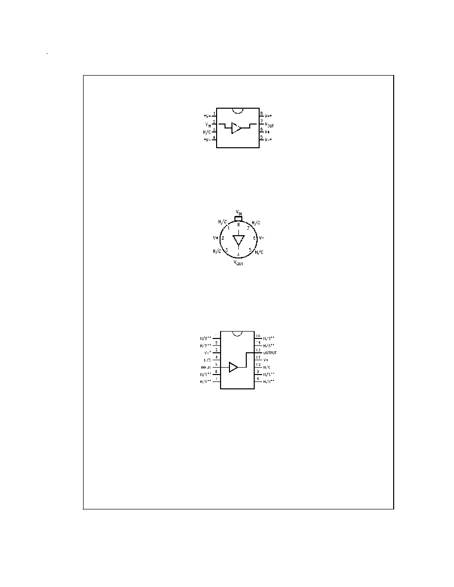
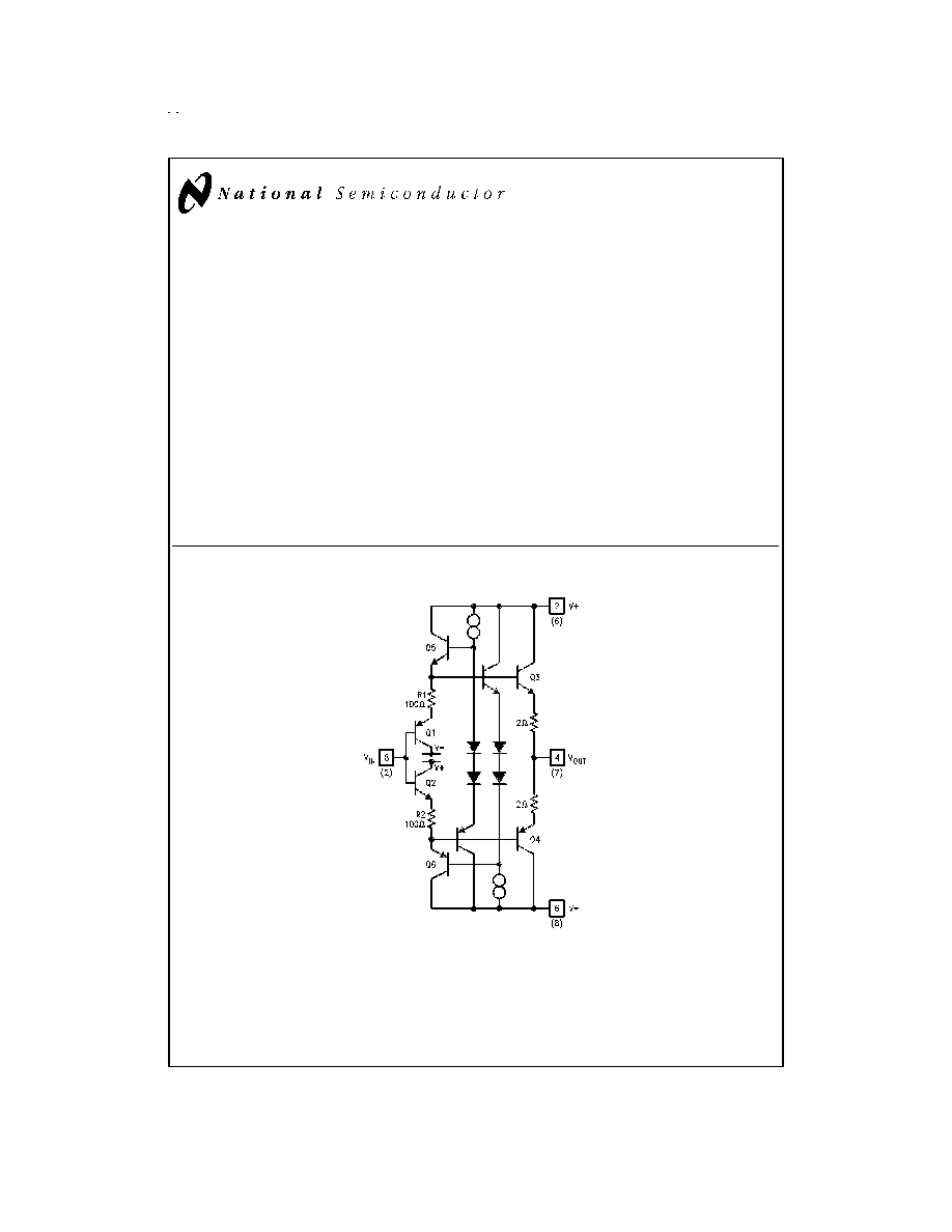
Simplified Schematic
VIP
TM
is a trademark of National Semiconductor Corporation.
DS009223-1
Numbers in ( ) are for 8-pin N DIP.
May 1998
LM6121/LM6221/LM6321
High
Speed
Buffer
© 1999 National Semiconductor Corporation
DS009223
www.national.com

Absolute Maximum Ratings
(Note 1)
If Military/Aerospace specified devices are required,
please contact the National Semiconductor Sales Office/
Distributors for availability and specifications.
Supply Voltage
36V (
±
18)
Input to Output Voltage (Note 2)
±
7V
Input Voltage
±
Vsupply
Output Short-Circuit to GND
Continuous
(Note 3)
Storage Temperature Range
-65°C to +150°C
Lead Temperature
(Soldering, 10 seconds)
260°C
Power Dissipation
(Note 10)
ESD Tolerance (Note 8)
±
2000V
Junction Temperature (T
J(max)
)
150°C
Operating Ratings
Operating Temperature Range
LM6121H/883
-55°C to +125°C
LM6221
-40°C to +85°C
LM6321
0°C to +70°C
Operating Supply Range
4.75 to
±
16V
Thermal Resistance (
JA
), (Note 4)
H Package
150°C/W
N Package
47°C/W
M Package
69°C/W
Thermal Resistance (
JC
), H Package
17°C/W
DC Electrical Characteristics
The following specifications apply for Supply Voltage =
±
15V, V
CM
= 0, R
L
100 k
and R
S
= 50
unless otherwise noted.
Boldface limits apply for T
A
= T
J
= T
MIN
to T
MAX
; all other limits T
A
= T
J
= 25°C.
Symbol
Parameter
Conditions
Typ
LM6121
LM6221
LM6321
Units
Limit
Limit
Limit
(Notes 5, 9)
(Note 5)
(Note 5)
A
V1
Voltage Gain 1
R
L
= 1 k
, V
IN
=
±
10V
0.990
0.980
0.980
0.970
0.970
0.950
0.950
A
V2
Voltage Gain 2
R
L
= 50
, V
IN
=
±
10V
0.900
0.860
0.860
0.850
V/V
0.800
0.820
0.820
Min
A
V3
Voltage Gain 3
R
L
= 50
,
V
+
= 5V
0.840
0.780
0.780
0.750
(Note 6)
V
IN
= 2 V
pp
(1.5 V
pp
)
0.750
0.700
0.700
V
OS
Offset Voltage
R
L
= 1 k
15
30
30
50
mV
50
60
100
Max
I
B
Input Bias Current
R
L
= 1 k
, R
S
= 10 k
1
4
4
5
µA
7
7
7
Max
R
IN
Input Resistance
R
L
= 50
5
M
C
IN
Input Capacitance
3.5
pF
R
O
Output Resistance
I
OUT
=
±
10 mA
3
5
5
5
10
10
6
Max
I
S1
Supply Current 1
R
L
=
15
18
18
20
mA
Max
20
20
22
I
S2
Supply Current 2
R
L
=
, V
+
= 5V
14
16
16
18
18
18
20
V
O1
Output Swing 1
R
L
= 1k
13.5
13.3
13.3
13.2
13
13
13
V
O2
Output Swing 2
R
L
= 100
12.7
11.5
11.5
11
±
V
10
10
10
Min
V
O3
Output Swing 3
R
L
= 50
12
11
11
10
9
9
9
V
O4
Output Swing 4
R
L
= 50
,
V
+
= 5V
1.8
1.6
1.6
1.6
V
PP
(Note 6)
1.3
1.4
1.5
Min
PSSR
Power Supply
V
±
=
±
5V to
±
15V
70
60
60
60
dB
Rejection Ratio
55
50
50
Min
www.national.com
3
AC Electrical Characteristics
The following specifications apply for Supply Voltage =
±
15V, V
CM
= 0, R
L
100 k
and R
S
= 50
unless otherwise noted.
Boldface limits apply for T
A
= T
J
= T
MIN
to T
MAX
; all other limits T
A
= T
J
= 25°C.
Symbol
Parameter
Conditions
Typ
LM6121
LM6221
LM6321
Units
Limit
Limit
Limit
(Note 5)
(Note 5)
(Note 5)
SR
1
Slew Rate 1
V
IN
=
±
11V, R
L
= 1 k
1200
550
550
550
V/µs
Min
SR
2
Slew Rate 2
V
IN
=
±
11V, R
L
= 50
800
550
550
550
(Note 7)
SR
3
Slew Rate 3
V
IN
= 2 V
PP
, R
L
= 50
50
550
550
550
V
+
= 5V (Note 6)
BW
-3 dB Bandwidth
V
IN
=
±
100 mV
PP
, R
L
= 50
50
30
30
30
MHz
C
L
10 pF
Min
t
r
, t
f
Rise Time
R
L
= 50
, C
L
10 pF
7.0
ns
Fall Time
V
O
= 100 mV
PP
t
pd
Propagation
R
L
= 50
, C
L
10 pF
4.0
ns
Delay Time
V
O
= 100 mV
PP
O
S
Overshoot
R
L
= 50
, C
L
10 pF
10
%
V
O
= 100 mV
PP
Note 1: Absolute Maximum Ratings indicate limits beyond which damage to the device may occur. DC and AC electrical specifications do not apply when operating
the device beyond its rated operating conditions.
Note 2: During current limit or thermal limit, the input current will increase if the input to output differential voltage exceeds 8V. For input to output differential voltages
in excess of 8V the input current should be limited to
±
20 mA.
Note 3: The LM6121 series buffers contain current limit and thermal shutdown to protect against fault conditions.
Note 4: The thermal resistance
JA
of the device in the N package is measured when soldered directly to a printed circuit board, and the heat-sinking pins (pins 1,
4, 5 and 8) are connected to 2 square inches of 2 oz. copper. When installed in a socket, the thermal resistance
JA
of the N package is 84°C/W. The thermal re-
sistance
JA
of the device in the M package is measured when soldered directly to a printed circuit board, and the heat-sinking pins (pins 1, 2, 6, 7, 8, 9, 13, 14) are
connected to 1 square inch of 2 oz. copper.
Note 5: Limits are guaranteed by testing or correlation.
Note 6: The input is biased to 2.5V and V
IN
swings V
pp
about this value. The input swing is 2 V
pp
at all temperatures except for the A
V
3 test at -55°C where it is
reduced to 1.5 V
pp
.
Note 7: Slew rate is measured with a
±
11V input pulse and 50
source impedance at 25°C. Since voltage gain is typically 0.9 driving a 50
load, the output swing
will be approximately
±
10V. Slew rate is calculated for transitions between
±
5V levels on both rising and falling edges. A high speed measurement is done to minimize
device heating. For slew rate versus junction temperature see typical performance curves. The input pulse amplitude should be reduced to
±
10V for measurements
at temperature extremes. For accurate measurements, the input slew rate should be at least 1700 V/µs.
Note 8: The test circuit consists of the human body model of 120 pF in series with 1500
.
Note 9: For specification limits over the full Military Temperature Range, see RETS6121X.
Note 10: The maximum power dissipation is a function of T
J(max)
,
JA
, and T
A
. The maximum allowable power dissipation at any ambient temperature is P
D
=
(T
J(max)
T
A
)/
JA
.
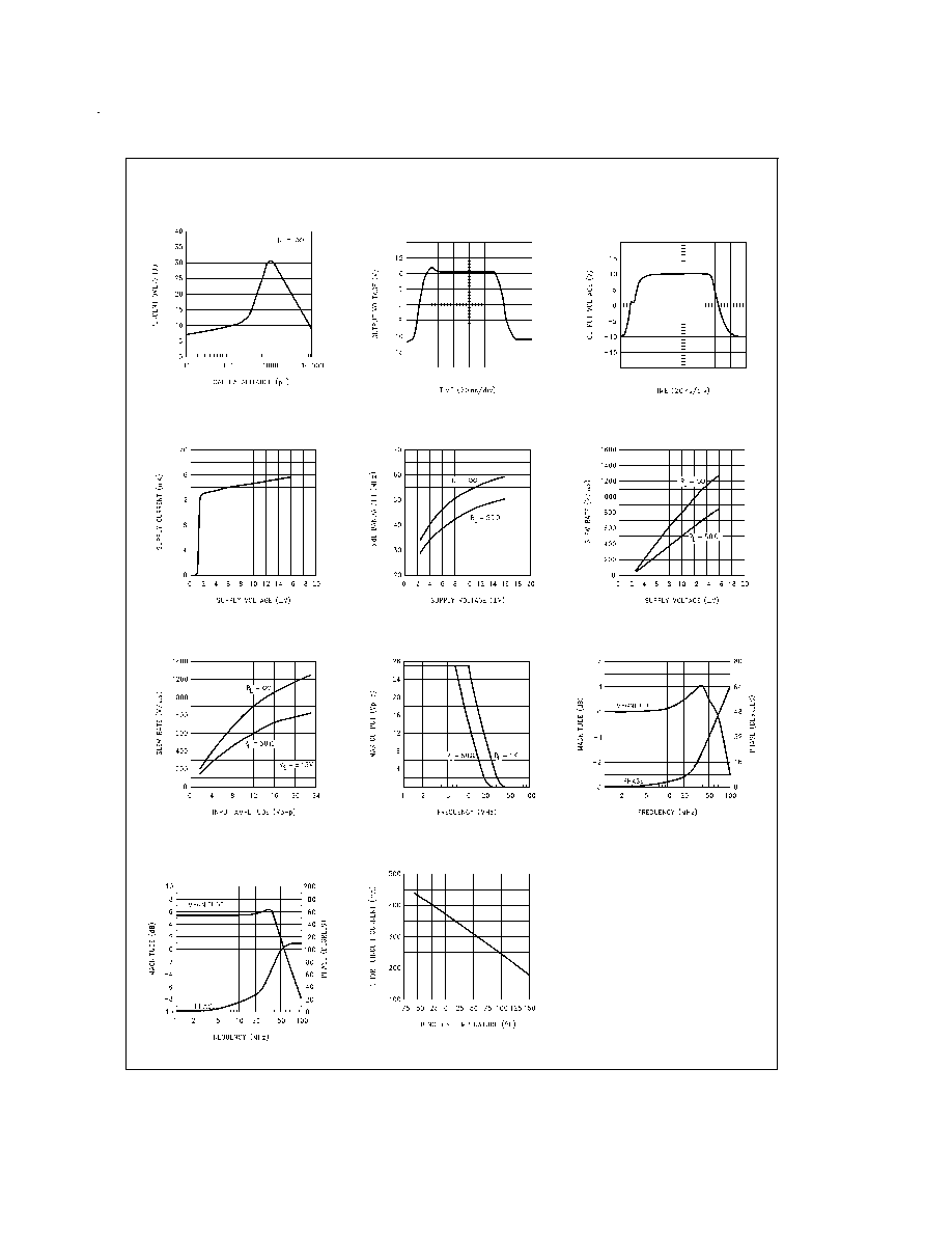
Typical Performance Characteristics
T
J
= 25°C, unless otherwise specified
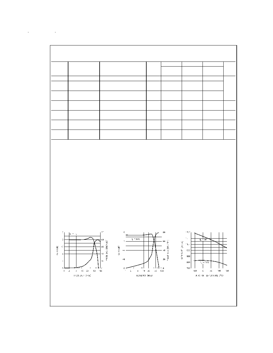
Frequency Response
DS009223-11
Frequency Response
DS009223-12
Slew Rate vs Temperature
DS009223-13
www.national.com
4