 | –≠–ª–µ–∫—Ç—Ä–æ–Ω–Ω—ã–π –∫–æ–º–ø–æ–Ω–µ–Ω—Ç: LM1042 | –°–∫–∞—á–∞—Ç—å:  PDF PDF  ZIP ZIP |

TL H 8709
LM1042
Fluid
Level
Detector
February 1995
LM1042 Fluid Level Detector
General Description
The LM1042 uses the thermal-resistive probe technique to
measure the level of non-flammable fluids An output is pro-
vided proportional to fluid level and single shot or repeating
measurements may be made All supervisory requirements
to control the thermal-resistive probe including short and
open circuit probe detection are incorporated within the de-
vice A second linear input for alternative sensor signals
may also be selected
Features
Y
Selectable thermal-resistance or linear probe inputs
Y
Control circuitry for thermal-resistive probe
Y
Single-shot or repeating measurements
Y
Switch on reset and delay to avoid transients
Y
Output amplifier with 10 mA source and sink capability
Y
Short or open probe detection
Y
a
50V transient protection on supply and control input
Y
7 5V to 18V supply range
Y
Internally regulated supply
Y
b
40 C to
a
80 C operation
Block Diagram
TL H 8709 ≠ 1
C1995 National Semiconductor Corporation
RRD-B30M115 Printed in U S A
Absolute Maximum Ratings
If Military Aerospace specified devices are required
please contact the National Semiconductor Sales
Office Distributors for availability and specifications
Supply Voltage V
CC
32V
Voltage at Pin 8
32V
Positive Peak Voltage (Pins 6 8 3) (Note 1)
10 ms 2A
50V
Output Current Pin 4 (I
4
)(sink)
10 mA
Output Current Pin 11 (source)
25 mA
Output Current Pin 16
g
10 mA
Operating Temperature Range
b
40 C to
a
80 C
Storage Temperature Range
b
55 C to
a
150 C
Lead Temperature (Soldering 10 sec )
260 C
Package Power Dissipation
T
A
e
25 C (Note 8)
1 8W
Device Power Dissipation
0 9W
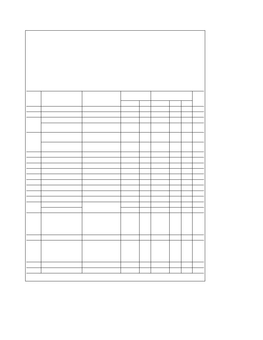
Electrical Characteristics
V
CC
e
13V T
A
within operating range except where stated otherwise C
T
e
22 mF R
T
e
12k
Tested Limits
Design Limits
Symbol
Parameter
Conditions
(Note 2)
(Note 3)
Units
Min
Max
Min
Typ
Max
V
CC
Supply Voltage
7 5
18
7 5
13
18
V
I
S
Supply Current
35
35
mA
V
REG
Regulated Voltage
Pins 15 and 11 connected
5 7
6 15
5 65
5 9
6 2
V
Stability Over V
CC
Range
Referred to value at
g
0 5
g
0 5
%
V
CC
e
13V (Note 4)
V
6
≠ V
3
Probe Current
2 15
2 35
2 10
2 25
2 40
V
Reference Voltage
Probe Current Regulation
(Note 4)
g
0 5
g
0 8
%
Over V
CC
Range
T
1
Ramp Timing
See
Figure 5
20
37
15
31
42
ms
T
2
≠ T
1
3
16
ms
T
4
≠ T
1
Ramp Timing
1 4
2 1
1 4
1 75
2 1
s
T
STAB
Ramp Timing Stability
Over V
CC
Range
a
5
g
5
%
R
T
Ramp Resistor Range
3
15
3
15 0
kX
V
8
Start Input Logic High Level
1 7
1 7
V
V
8
Start Input Logic Low Level
0 5
0 5
V
I
8
Start Input Current
V
8
e
V
CC
100
100
nA
I
8
Start Input Current
V
8
e
0V
300
300
nA
V
16
Maximum Output Voltage
R
L
e
600X from
V
REG
b
0 3
V
REG
b
0 3
V
Minimum Output Voltage
Pin 16 to V
REG
0 5
0 2
0 6
V
PROBE 1
G
1
Probe 1 Gain
Pin 1 80 mV to 520 mV
9 9
10 4
10 15
(Notes 6 7)
Non-linearity of G
1
Pin 1 80 mV to 520 mV
b
1
a
1
b
2
0
2
%
(Note 7)
OS
1
Pin 1 Offset
(Note 7)
g
5
mV
PROBE 2
G
2
Probe 2 Gain
Pin 7 240 mV to 1 562V
3 31
3 49
3 4
(Note 7)
Non-linearity of G
2
Pin 7 240 mV to 1 562V
b
1
a
1
b
2
0 2
2
%
(Note 7)
OS
7
Pin 7 Offset
(Note 7)
g
5
mV
R
7
Input impedance
5
MX
2

Electrical Characteristics
V
CC
e
13V T
A
within operating range except where stated otherwise C
T
e
22 mF R
T
e
12k (Continued)
Tested Limits
Design Limits
Symbol
Parameter
Conditions
(Note 2)
(Note 3)
Units
Min
Max
Min
Typ
Max
V
1
Probe 1 Input
V
CC
e
9V to 18V
1
5
1
5
V
Voltage Range
V
CC
e
7 5V I
4
k
2 5 mA
1
3 5
V
(V
REG
e
6 0V)
V
5
Probe 1 Open
At Pin 5
V
REG
b
0 7 V
REG
b
0 5 V
REG
b
0 85 V
REG
b
0 6 V
REG
b
0 35
V
Circuit Threshold
V
5
Probe 1 Short
0 5
0 7
0 35
0 6
0 85
V
Circuit Threshold
I
14
Pin 14 Input
Pin 14
e
4V
b
2 0
2 0
2 0
nA
Leakage Current
I
1
Pin 1 Input
Pin 1
e
300 mV
b
5 0
5 0
1 5
5 0
nA
Leakage Current
T
R
Repeat Period
C
R
e
22 mF (Note 5)
12
28
9 1
17
36
s
C
R
Discharge Time
C
R
e
22 mF
70
135
ms
C
M
Memory Capacitor Value
0 47
m
F
C
1
Input Capacitor Value
0 47
m
F
Sensitivity fo Electrostatic Discharge
Pins 7 10 13 and 14 will withstand greater than 1500V when tested using 100 pF and 1500X in accordance with National Semiconductor standard ESD test
procedures
All other pins will withstand in excess of 2 kV
Note 1
Test circuit for over voltage capability at pins 3 6 8
TL H 8709 ≠ 2
Note 2
Guaranteed and 100% production tested at 25 C These limits are used to calculate outgoing quality levels
Note 3
Limits guardbanded to include parametric variations T
A
e b
40 C to
a
80 C and from V
CC
e
7 5V to 18V These limits are not used to calculate AOQL
figures
Note 4
Variations over temperature range are not production tested
Note 5
Time for first repeat period see
Figure 6
Note 6
Probe 1 amplifier tests are measured with pin 12 ramp voltage held between the T
3
and T
4
conditions (pin 12
1 1V) having previously been held above
4 1V to simulate ramp action See Figure 5
Note 7
When measuring gain separate ground wire sensing is required at pin 2 to ensure sufficiently accurate results
Linearity is defined as the difference between the predicted value of V
B
(V
B
) and the measured value
Note 8
Above T
A
e
25 C derate with i
jA
e
70 C W
TL H 8709 ≠ 15
For probe 1 and probe 2
Gain (G)
e
V
C
b
V
A
V
c
b
V
a
Input offset
e
V
C
G
b
V
c
(
Linearity
e
V
B
V
B
b
1
(
c
100%
V
B
e
V
A
a
G(V
b
b
V
a
)
3

Typical Performance Characteristics
Supply Voltage
Supply Current vs
Supply Voltage
Regulated Voltage vs
Supply Voltage
Probe Reference V vs
Pin 7 Voltage
Output Voltage vs
Pin 14 Voltage
Output Voltage vs
TL H 8709 ≠ 3
Pin Function Description
Pin 1
Input amplifier for thermo-resistive probe with 5 nA
maximum leakage Clamped to ground at the start of
a probe 1 measurement
Pin 2
Device ground
0V
Pin 3
This pin is connected to the emitter of an external
PNP transistor to supply a 200 mA constant current
to the thermo-resistive probe An internal reference
maintains this pin at V
SUPPLY
b
2V
Pin 4
Base connection for the external PNP transistor
Pin 5
This pin is connected to the thermo-resistive probe
for short and open circuit probe detection
Pin 6
Supply pin
a
7 5V to
a
18V
protected against
a
50V transients
Pin 7
High Impedance input for second linear voltage
probe with an input range from 1V to 5V The gain
may be set externally using pin 10
Pin 8
Probe select and control input If this pin is taken to
a logic low level probe 1 is selected and the timing
cycle is initiated The selection logic is subsequently
latched low until the end of the measurement If kept
at a low level one shot or repeating probe 1 mea-
surements will be made depending upon pin 9 condi-
tions A high input level selects probe 2 except dur-
ing a probe 1 measurement period
Pin 9
The repeat oscillator timing capacitor is connected
from this pin to ground A 2 mA current charges up
the capacitor towards 4 3V when the probe 1 mea-
surement cycle is restarted If this pin is grounded
the repeat oscillator is disabled and only one probe
1 measurement will be made when pin 8 goes low
Pin 10 A resistor may be connected to ground to vary the
gain of the probe 2 input amplifier Nominal gain
when open circuit is 1 2 and when shorted to ground
3 4 DC conditions may be adjusted by means of a
resistor divider network to V
REG
and ground
Pin 11 Regulated voltage output Requires to be connected
to pin 15 to complete the supply regulator control
loop
Pin 12 The capacitor connected from this pin to ground
sets the timing cycle for probe 1 measurements
Pin 13 The resistor connected between this pin and ground
defines the charging current at pin 12 Typically 12k
the value should be within the range 3k to 15k
Pin 14 A low leakage capacitor typical value 0 1 mF and
not greater than 0 47 mF should be connected from
this pin to the regulated supply at pin 11 to act as a
memory capacitor for the probe 1 measurement
The internal leakage at this pin is 2 nA max for a
long memory retention time
Pin 15 Feedback input for the internal supply regulator nor-
mally connected to V
REG
at pin 11 A resistor may
be connected in series to adjust the regulated output
voltage by an amount corresponding to the 1 mA
current into pin 15
Pin 16 Linear voltage output for probe 1 and probe 2 capa-
ble of driving up to
g
10 mA May be connected with
a 600X meter to V
REG
4

Application Notes
THERMO-RESISTIVE PROBES
OPERATION AND
CONSTRUCTION
These probes work on the principle that when power is dis-
sipated within the probe the rise in probe temperature is
dependent on the thermal resistance of the surrounding ma-
terial and as air and other gases are much less efficient
conductors of heat than liquids such as water and oil it is
possible to obtain a measurement of the depth of immersion
of such a probe in a liquid medium This principle is illustrat-
ed in
Figure 1
TL H 8709 ≠ 4
FIGURE 1
During the measurement period a constant current drive I is
applied to the probe and the voltage across the probe is
sampled both at the start and just before the end of the
measurement period to give DV R
TH
Air and R
TH
Oil repre-
sent the different thermal resistances from probe to ambient
in air or oil giving rise fo temperature changes DT
1
and DT
2
respectively As a result of these temperature changes the
probe resistance will change by DR
1
or DR
2
and give corre-
sponding voltage changes DV
1
or DV
2
per unit length
Hence
D
V
e
L
A
L
D
V
1
a
(L
b
L
A
)
L
D
V
2
and for DV
1
l
D
V
2
R
TH
Air
l
R
TH
Oil DV will increase as
the probe length in air increases For best results the probe
needs to have a high temperature coefficient and low ther-
mal time constant One way to achieve this is to make use
of resistance wires held in a suitable support frame allowing
free liquid access Nickel cobalt iron alloy resistance wires
are available with resistivity 50 mXcm and 3300 ppm tem-
perature coefficient which when made up into a probe with 4
c
2 cm 0 08 mm diameter strands between supports (10
cm total) can give the voltage vs time curve shown in
Figure
2 for 200 mA probe current The effect of varying the probe
current is shown in
Figure 3 To avoid triggering the probe
failure detection circuits the probe voltage must be between
0 7V and 5 3V (V
REG
b
6V) hence for 200 mA the permis-
sible probe resistance range is from 3 5X to 24X The ex-
ample given has a resistance at room temperature of 9X
which leaves plenty of room for increase during measure-
ments and changes in ambient temperature
Various arrangements of probe wire are possible for any
given wire gauge and probe current to suit the measurement
range required some examples are illustrated schematically
in
Figure 4 Naturally it is necessary to reduce the probe
TL H 8709 ≠ 5
FIGURE 2
current with very fine wires to avoid excessive heating and
this current may be optimized to suit a particular type of
wire The temperature changes involved will give rise to no-
ticeable length changes in the wire used and more sophisti-
cated holders with tensioning devices may be devised to
allow for this
TL H 8709 ≠ 6
FIGURE 3
Probes need not be limited to resistance wire types as any
device with a positive temperature coefficient and sufficient-
ly low thermal resistance to the encapsulation so as not to
mask the change due to the different surrounding mediums
could be used Positive temperature coefficient thermistors
are a possibility and while their thermal time constant is like-
ly to be longer than wire the measurement time may be
increased by changing C
T
to suit
TL H 8709 ≠ 7
FIGURE 4
5