TL F 5845
DS7880DS8880
High
Voltage
7-Segment
DecoderDriver
March 1988
DS7880 DS8880 High Voltage 7-Segment Decoder Driver
General Description
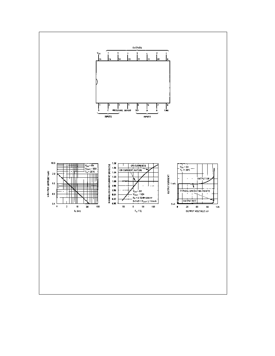
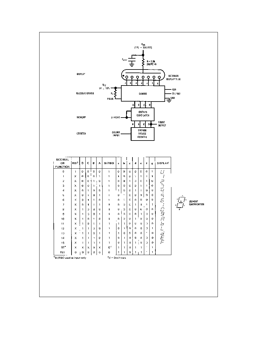
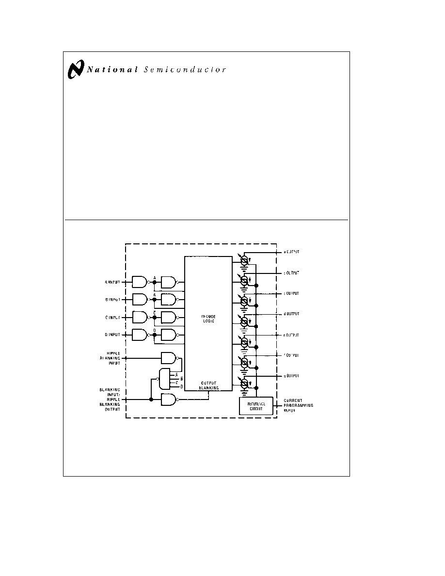
The DS7880 DS8880 is custom designed to decode four
lines of BCD and drive a gas-filled seven-segment display
tube
Each output constitutes a switchable adjustable current
sink which provides constant current to the tube segment
even with high tube anode supply tolerance or fluctuation
These current sinks have a voltage compliance from 3V to
at least 80V typically the output current varies 1% for out-
put voltage changes of 3 to 50V Each bit line of the decod-
er switches a current sink on or off as prescribed by the
input code Each current sink is ratioed to the b-output cur-
rent as required for even illumination of all segments
Output currents may be varied over the 0 2 to 1 5 mA range
for driving various tube types or multiplex operation The
output current is adjusted by connecting an external pro-
gram resistor (R
P
) from V
CC
to the Program input in accord-
ance with the programming curve The circuit design pro-
vides a one-to-one correlation between program input cur-
rent and b-segment output current
The Blanking Input provides unconditional blanking of any
output display while the Ripple Blanking pins allow simple
leading- or trailing-zero blanking
Features
Y
Current sink outputs
Y
Adjustable output current
0 2 to 1 5 mA
Y
High output breakdown voltage
110V typ
Y
Suitable for multiplex operation
Y
Blanking and Ripple Blanking provisions
Y
Low fan-in and low power
Logic Diagram
TL F 5845 ≠ 1
C1995 National Semiconductor Corporation
RRD-B30M105 Printed in U S A

Absolute Maximum Ratings
(Note 1)
If Military Aerospace specified devices are required
please contact the National Semiconductor Sales
Office Distributors for availability and specifications
V
CC
7V
Input Voltage (Except BI)
6V
Input Voltage (BI)
V
CC
Segment Output Voltage
80V
Power Dissipation
600 mW
Maximum Power Dissipation at 25 C
Cavity Package
1509 mW
Molded Package
1476 mW
Derate cavity package 10 06 mW C above 25 C derate molded package
11 81 mW C above 25 C
Transient Segment Output Current
(Note 4)
50 mA
Storage Temperature Range
b
65 C to
a
150 C
Lead Temperature (Soldering 4 sec )
260 C
Operating Conditions
Min
Max
Units
Supply Voltage (V
CC
)
DS7880
4 5
5 5
V
DS8880
4 75
5 25
V
Temperature (T
A
)
DS7880
b
55
a
125
C
DS8880
0
a
70
C
Electrical Characteristics
(Notes 2 and 3)
Symbol
Parameter
Conditions
Min
Typ
Max
Units
V
IH
Logical ``1'' Input Voltage
V
CC
e
Min
2 0
V
V
IL
Logical ``0'' Input Voltage
V
CC
e
Min
0 8
V
V
OH
Logical ``1'' Output Voltage
V
CC
e
Min I
OUT
e b
200 mA RBO
2 4
3 7
V
V
OL
Logical ``0'' Output Voltage
V
CC
e
Min I
OUT
e
8 mA RBO
0 13
0 4
V
I
IH
Logical ``1'' Input Current
V
CC
e
Max Except BI
V
IN
e
2 4V
2
15
m
A
V
IN
e
5 5V
4
400
m
A
I
IL
Logical ``0'' Input Current
V
CC
e
Max V
IN
e
0 4V
Except BI
b
300
b
600
m
A
BI
b
1 2
b
2 0
mA
I
CC
Power Supply Current
V
CC
e
Max R
p
e
2 2k All Inputs
e
0V
27
43
mA
V
CD
Input Diode Clamp Voltage
V
CC
e
Max T
A
e
25 C I
IN
e
12 mA
b
0 9
b
1 5
V
I
O
SEGMENT OUTPUTS
All Outputs
e
50V
Outputs a f and g
0 84
0 93
1 02
``ON'' Current Ratio
I
OUT
b
e
Ref
Outut c
1 12
1 25
1 38
Output d
0 90
1 00
1 10
Output e
0 99
1 10
1 21
I
b
ON
Output b ``ON'' Current
V
CC
e
5V V
OUT
b
e
50V
R
p
e
18 1k
0 15
0 20
0 25
mA
All Other Outputs
t
5V
R
p
e
7 03k
0 45
0 50
0 55
mA
T
A
e
25 C
R
p
e
3 40k
0 90
1 00
1 10
mA
R
p
e
2 20k
1 35
1 50
1 65
mA
V
SAT
Output Saturation Voltage
V
CC
e
Min R
p
e
1k
g
5% I
OUT
b
e
2 mA (Note 5)
0 8
2 5
V
I
CEX
Output Leakage Current
V
OUT
e
75V BI
e
0V R
p
e
2 2k
0 003
3
m
A
V
BR
Output Breakdown Voltage
I
OUT
e
250 mA BI
e
0V R
p
e
2 2k
80
110
V
t
pd
Propagation Delays BCD
V
CC
e
5V T
A
e
25 C
0 4
10
m
s
Input to Segment Output
BI to Segment Output
0 4
10
m
s
RBI to Segment Output
0 7
10
m
s
RBI to RBO
0 4
10
m
s
Note 1
``Absolute Maximum Rating'' are those values beyond which the safety of the device cannot be guaranteed They are not meant to imply that the devices
should be operated at these limits The table of ``Electrical Characteristics'' provides conditions for actual device operation
Note 2
Unless otherwise specified min max limits apply across the
b
55 C to
a
125 C temperature range for the DS7880 and across the 0 C to
a
70 C range for
the DS8880 All typical values are for T
A
e
25 C and V
CC
e
5V
Note 3
All currents into device pins shown as positive out of device pins as negative all voltages referenced to ground unless otherwise noted All values shown
as max or min or absolute value basis
Note 4
In all applications transient segment output current must be limited to 50 mA This may be accomplished in dc applications by connecting a 2 2k resistor
from the anode-supply filter capacitor to the display anode or by current limiting the anode driver in multiplex applications
Note 5
For saturation mode the segment output currents are externally limited and ratioed
2